The information in this document is subject to change without notice. Before using this document, please
confirm that this is the latest version.
Not all devices/types available in every country. Please check with local NEC representative for
availability and additional information.
1998
©
Document No. D15599EJ2V0DS00 (2nd edition)
Date Published April 2002 N CP(K)
Printed in Japan
SILICON POWER TRANSISTOR
2SC4553
NPN SILICON EPITAXIAL TRANSISTOR
FOR HIGH-SPEED SWITCHING
DATA SHEET
2002
The 2SC4553 is a power transistor designed especially for low
collector saturation voltage and features large current switching at a
low power dissipation. In addition, a high h
FE
enables alleviation of
the driver load.
FEATURES
∑ High h
FE
and low V
CE(sat)
:
h
FE
800 (V
CE
= 2 V, I
C
= 3 A)
V
CE(sat)
0.12 V (I
C
= 3 A, I
B
= 0.03 A)
∑ On-chip C to E damper diode
∑ Mold package that does not require an insulating board or
insulation bushing
ABSOLUTE MAXIMUM RATINGS (Ta = 25
∞
∞
∞
∞C)
Parameter
Symbol
Ratings
Unit
Collector to base voltage
V
CBO
100
V
Collector to emitter voltage
V
CEO
100
V
Emitter to base voltage
V
EBO
7.0
V
Collector current (DC)
I
C(DC)
±7.5
A
Collector current (pulse)
I
C(pulse)
*
±10
A
Base current (DC)
I
B(DC)
2.0
A
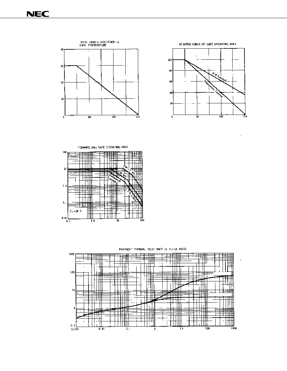
Total power dissipation
P
T
(Tc = 25
∞C)
30
W
Total power dissipation
P
T
(Ta = 25
∞C)
2.0
W
Junction temperature
T
j
150
∞C
Storage temperature
T
stg
-55 to +150
∞C
* PW
10 ms, duty cycle 50%
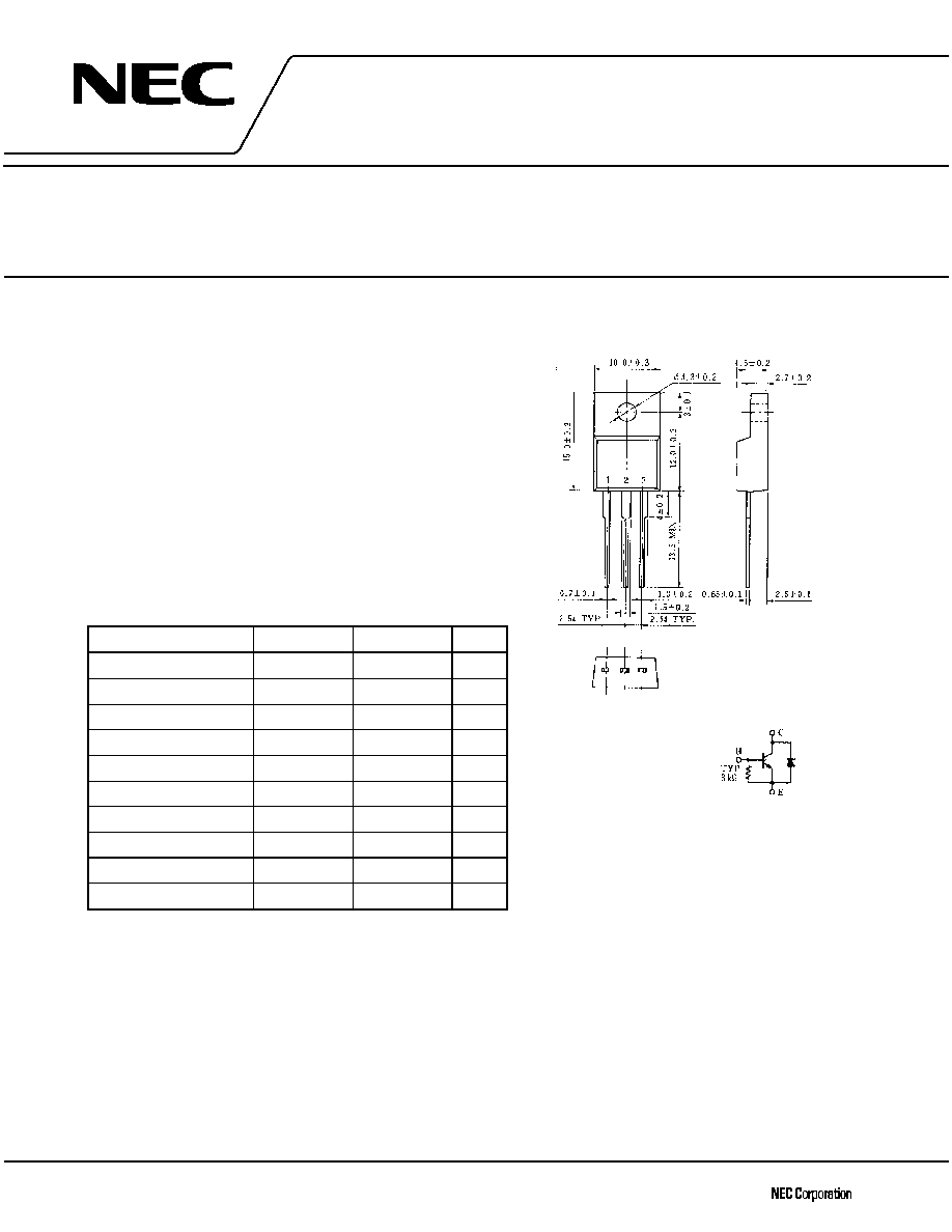
PACKAGE DRAWING (UNIT: mm)
(OHFWURGH &RQQHFWLRQ
%DVH
&ROOHFWRU
(PLWWHU
(48,9$/(17 &,5&8,7
Data Sheet D15599EJ2V0DS
2
6&
ELECTRICAL CHARACTERISTICS (Ta = 25
∞
∞
∞
∞C)
3DUDPHWHU
6\PERO
&RQGLWLRQV
0,1
7<3
0$;
8QLW
&ROOHFWRU FXWRII FXUUHQW
,
&%2
9
&%
9 ,
(
µ$
(PLWWHU FXWRII FXUUHQW
,
(%2
9
(%
9 ,
&
P$
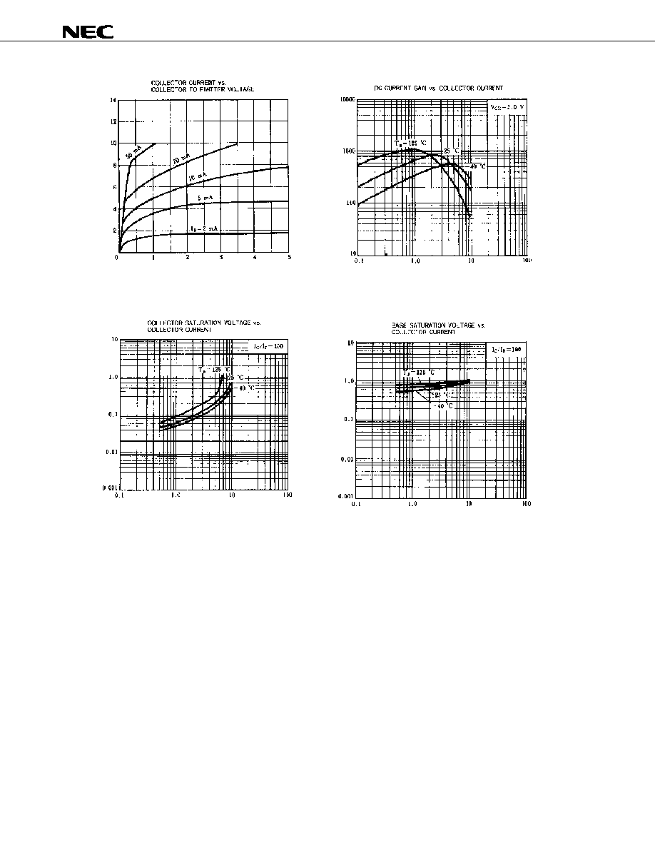
'& FXUUHQW JDLQ
K
)(
9
&(
9 ,
&
$
'& FXUUHQW JDLQ
K
)(
9
&(
9 ,
&
$
&ROOHFWRU VDWXUDWLRQ YROWDJH
9
&(VDW�
,
&
$ ,
%
P$
9
&ROOHFWRU VDWXUDWLRQ YROWDJH
9
&(VDW�
,
&
$ ,
%
P$
9
&ROOHFWRU VDWXUDWLRQ YROWDJH
9
&(VDW�
,
&
$ ,
%
P$
9
&ROOHFWRU VDWXUDWLRQ YROWDJH
9
&(VDW�
,
&
$ ,
%
P$
9
%DVH VDWXUDWLRQ YROWDJH
9
%(VDW�
,
&
$ ,
%
P$
9
*DLQ EDQGZLGWK SURGXFW
I
7
9
&(
9 ,
&
$
0+]
&ROOHFWRU FDSDFLWDQFH
&
RE
9
&%
9 ,
(
I 0+]
S)
7XUQRQ WLPH
W
RQ
µV
6WRUDJH WLPH
W
VWJ
µV
)DOO WLPH
W
I
,
&
$ 5
/
,
%
-,
%
P$ 9
&&
9
5HIHU WR WKH WHVW FLUFXLW
µV
'LRGH IRUZDUG YROWDJH
9
')
,
')
$
9
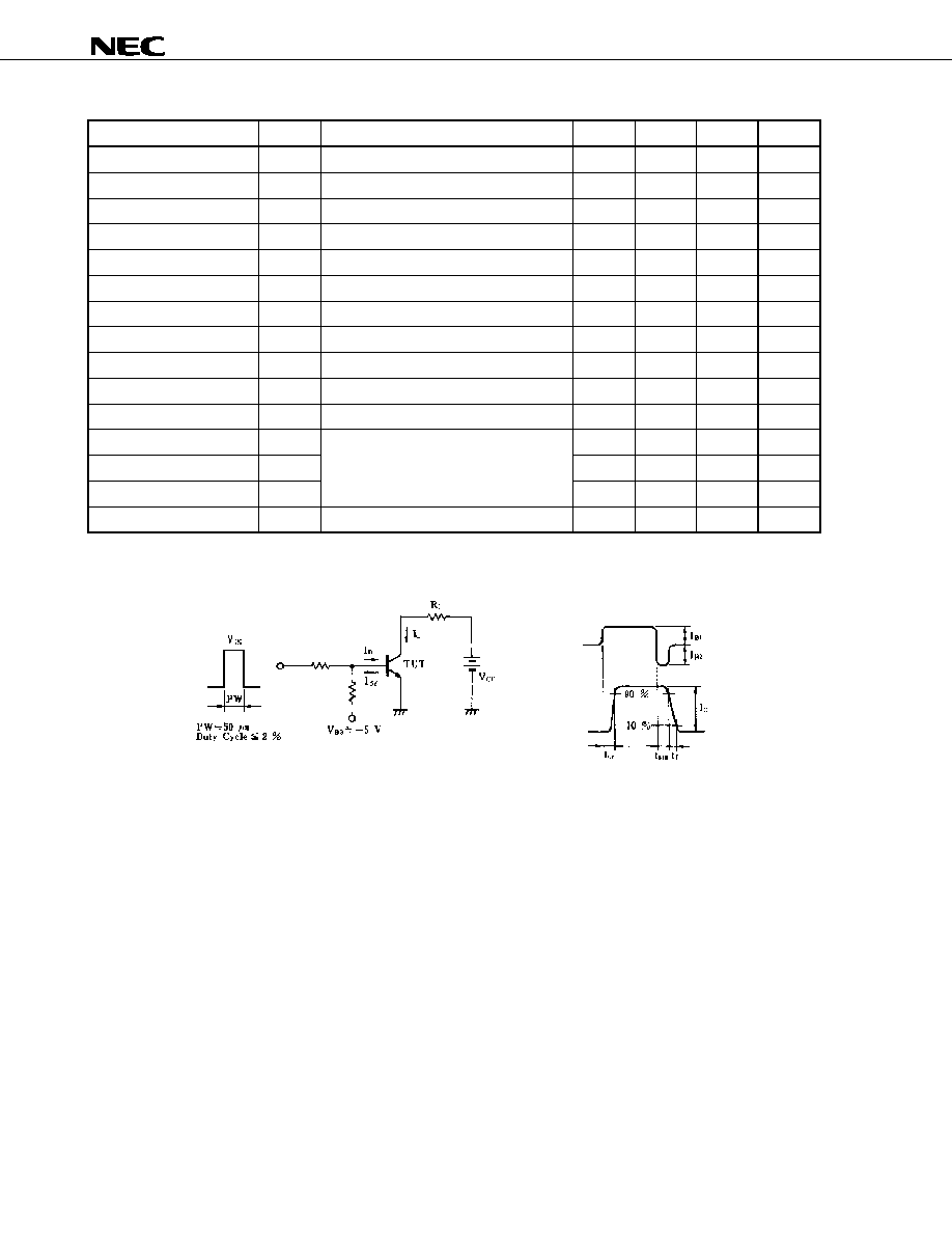
SWITCHING TIME (t
RQ
, t
VWJ
, t
I
) TEST CIRCUIT
%DVH FXUUHQW
ZDYHIRUP
&ROOHFWRU FXUUHQW
ZDYHIRUP