The information in this document is subject to change without notice. Before using this document, please
confirm that this is the latest version.
Not all devices/types available in every country. Please check with local NEC representative for
availability and additional information.
1998
©
Document No. D15605EJ3V0DS00 (3rd edition)
Date Published April 2002 N CP(K)
Printed in Japan
SILICON POWER TRANSISTOR
2SC4815
NPN SILICON
EPITAXIAL TRANSISTOR
FOR HIGH-SPEED SWITCHING
DATA SHEET
2002
The 2SC4815 is a power transistor developed for high-speed switching and features low V
CE(sat)
and high h
FE
.
This transistor is ideal for use as a driver in DC/DC converters and actuators.
In addition, this transistor is available for the auto mount in the radial taping specifications and for mounting cost
reduction.
FEATURES
∑ High h
FE
and low V
CE(sat)
:
V
CE(sat)
0.3 V @I
C
= 3.0 A, I
B
= 0.15 A
h
FE
100
@V
CE
= 2.0 V, I
C
= 1.0 A
∑ Available for auto mount in radial taping specifications
ABSOLUTE MAXIMUM RATINGS (Ta = 25
∞
∞
∞
∞C)
Parameter
Symbol
Ratings
Unit
Collector to base voltage
V
CBO
100
V
Collector to emitter voltage
V
CEO
60
V
Emitter to base voltage
V
EBO
7.0
V
Collector current (DC)
I
C(DC)
5.0
A
Collector current (pulse)
I
C(pulse)
*
10
A
Base current (DC)
I
B(DC)
2.5
A
Total power dissipation
P
T
1.8
W
Junction temperature
T
j
150
∞C
Storage temperature
T
stg
-55 to +150
∞C
* PW
300
µs, duty cycle 10%
Data Sheet D15605EJ3V0DS
2
2SC4815
ELECTRICAL CHARACTERISTICS (Ta = 25
∞
∞
∞
∞C)
Parameter
Symbol
Conditions
MIN.
TYP.
MAX.
Unit
Collector to emitter voltage
V
CEO(SUS)
I
C
= 5.0 A, I
B
= 0.5 A, L = 1 mH
60
V
Collector to emitter voltage
V
CEX(SUS)
I
C
= 2.5 A, I
B1
=
-I
B2
= 0.25 A
V
BE(OFF)
=
-1.5 V, L = 180
µH, Clamped
60
V
Collector cutoff current
I
CBO
V
CB
= 100 V, I
E
= 0
10
µA
Emitter cutoff current
I
EBO
V
EB
= 7.0 V, I
C
= 0
10
µA
DC current gain
h
FE1
*
V
CE
= 2.0 V, I
C
= 0.5 A
100
DC current gain
h
FE2
*
V
CE
= 2.0 V, I
C
= 1.0 A
100
200
400
DC current gain
h
FE3
*
V
CE
= 2.0 V, I
C
= 3.0 A
60
Collector saturation voltage
V
CE(sat)1
*
I
C
= 3.0 A, I
B
= 0.15 A
0.15
0.3
V
Collector saturation voltage
V
CE(sat)2
*
I
C
= 4.0 A, I
B
= 0.2 A
0.3
0.5
V
Base saturation voltage
V
BE(sat)1
*
I
C
= 3.0 A, I
B
= 0.15 A
0.9
1.2
V
Base saturation voltage
V
BE(sat)2
*
I
C
= 4.0 A, I
B
= 0.2 A
1.2
1.5
V
Collector capacitance
C
ob
V
CB
= 10 V, I
E
= 0 , f = 1.0 MHz
70
pF
Gain bandwidth product
f
T
V
CE
= 10 V, I
C
= 0.5 A
150
MHz
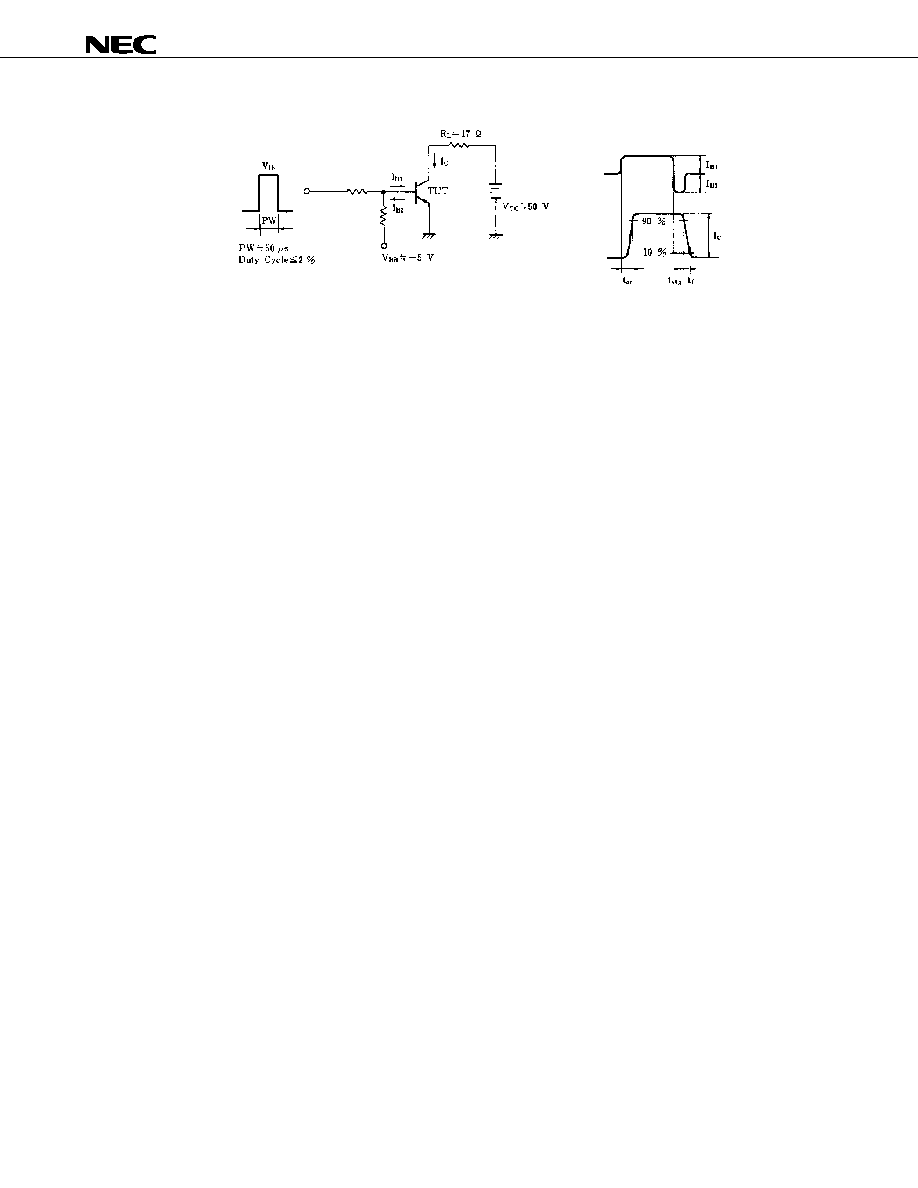
Turn-on time
t
on
0.1
µs
Storage time
t
stg
1.0
µs
Fall time
t
f
I
C
= 3.0 A, R
L
= 17
,
I
B1
=
-I
B2
= 0.15 A, V
CC
50 V
Refer to the test circuit.
0.25
µs
* Pulse test PW
350
µs, duty cycle 2%
h
FE
CLASSIFICATION
Marking
M
L
K
h
FE2
100 to 200
150 to 300
200 to 400
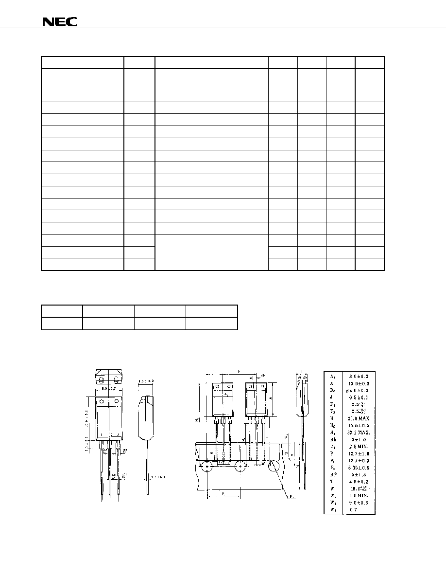
PACKAGE DRAWING (UNIT: mm)
TAPING SPECIFICATION
(OHFWURGH &RQQHFWLRQ
%DVH
&ROOHFWRU
(PLWWHU
or less

Data Sheet D15605EJ3V0DS
3
2SC4815
TYPICAL CHARACTERISTICS (Ta = 25
∞
∞
∞
∞C)
7
R
WD
O
3
R
Z
H
U
'
L
V
V
L
S
D
WL
R
Q
3
7
:
�
$PELHQW 7HPSHUDWXUH 7D ∞&�
3XOVH WHVW
&ROOHFWRU WR (PLWWHU 9ROWDJH 9
&(
9�
&DVH 7HPSHUDWXUH 7F ∞&�
,
&
'
HU
DW
L
Q
J
G
7
�
&R
OO
H
F
WR
U
&XU
U
H
Q
W
,
&
$
�
3XOVH :LGWK 3: V�
&ROOHFWRU WR (PLWWHU 9ROWDJH 9
&(
9�
&ROOHFWRU &XUUHQW ,
&
$�
6LQJOH SXOVH
7
U
DQV
L
H
QW
7
K
H
UP
DO
5
HV
L
V
W
DQF
H
5
WK
MD
�
∞
&
:
�
'
&
&XUU
H
Q
W*
D
L
Q
K
)(
&R
OO
H
F
WR
U
&XU
U
H
Q
W
,
&
$
�