 | –≠–ª–µ–∫—Ç—Ä–æ–Ω–Ω—ã–π –∫–æ–º–ø–æ–Ω–µ–Ω—Ç: 2SC4958 | –°–∫–∞—á–∞—Ç—å:  PDF PDF  ZIP ZIP |

PART
NUMBER
Embossed tape 8 mm wide.
2SC4958≠T1
3 Kpcs/Reel.
Pin3 (Collector) face to perfora-
tion side of the tape.
Embossed tape 8 mm wide.
2SC4958≠T2
3 Kpcs/Reel.
Pin1 (Emitter), Pin2 (Base) face
to perforation side of the tape.
©
1992
DATA SHEET
The mark 5 shows revised points.
SILICON TRANSISTOR
2SC4958
Caution; Electrostatic sensitive Device.
HIGH FREQUENCY LOW NOISE AMPLIFIER
NPN SILICON EPITAXIAL TRANSISTOR
SUPER MINI MOLD
Document No. P10380EJ2V0DS00 (2nd edition)
(Previous No. TD≠2409)
Date Published July 1995 P
Printed in Japan
1995
FEATURES
∑
Low Noise, High Gain
∑
Low Voltage Operation
∑
Low Feedback Capacitance
C
re
= 0.3 pF TYP.
ORDERING INFORMATION
QUANTITY
PACKING STYLE
* Please contact with responsible NEC person, if you require evaluation sample.
Unit sample quantity shall be 50 pcs. (Part No.: 2SC4958)
1.25
±
0.1
2.1
±
0.1
2.0
±
0.2
0.3
≠0
+0.1
0.65
0.65
0.3
≠0
+0.1
2
1
3
0.9
±
0.1
0.3
0.15
≠0.05
+0.1
0 to 0.1
Marking
PACKAGE DIMENSIONS
in millimeters
PIN CONNECTIONS
1.
2.
3.
Emitter
Base
Collector
ABSOLUTE MAXIMUM RATINGS (T
A
= 25
∞
C)
Collector to Base Voltage
V
CBO
9
V
Collector to Emitter Voltage
V
CEO
6
V
Emitter to Base Voltage
V
EBO
2
V
Collector Current
I
C
10
mA
Total Power Dissipation
P
T
60
mW
Junction Temperature
T
j
150
∞
C
Storage Temperature
T
stg
≠65 to +150
∞
C
2SC4958
2
ELECTRICAL CHARACTERISTICS (T
A
= 25
∞
C)
CHARACTERISTIC
SYMBOL
MIN.
TYP.
MAX.
UNIT
TEST CONDITION
Collector Cutoff Current
I
CBO
0.1
µ
A
V
CB
= 5 V, I
E
= 0
Emitter Cutoff Current
I
EBO
0.1
µ
A
V
EB
= 1 V, I
C
= 0
DC Current Gain
h
FE
75
150
V
CE
= 3 V, I
C
= 5 mA
*1
Gain Bandwidth Product
f
T
12
GHz
V
CE
= 3 V, I
C
= 5 mA, f = 2.0 GHz
Feed back Capacitance
C
re
0.3
0.5
pF
V
CB
= 3 V, I
E
= 0, f = 1 MHz
*2
Insertion Power Gain
|S
21e
|
2
7
8.5
dB
V
CE
= 3 V, I
C
= 5 mA, f = 2.0 GHz
Noise Figure
NF
2.5
4.0
dB
V
CE
= 3 V, I
C
= 3 mA, f = 2.0 GHz
*1
Pulse Measurement ; PW
350
µ
s, Duty Cycle
2 % Pulsed.
*2
Measured with 3 terminals bridge, Emitter and Case should be grounded.
h
FE
Classification
Rank
T82
Marking
T82
h
FE
75 to 150
TYPICAL CHARACTERISTICS (T
A
= 25
∞
C)
50
200
100
0
50
100
150
60 mW
40
30
20
10
0
0.5
1
V
CE
= 3 V
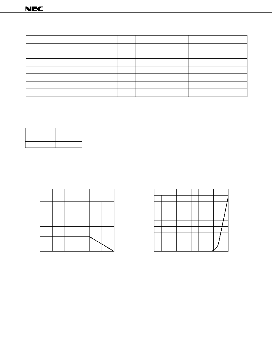
TOTAL POWER DISSIPATION
vs.AMBIENT TEMPERATURE
COLLECTOR CURRENT vs.
BASE TO EMITTER VOLTAGE
Free Air
P
T
≠ Total Power Dissipation ≠ mW
I
C
≠ Collector Current ≠ mA
T
A
≠ Ambient Temperature ≠ ∞C
V
BE
≠ Base to Emitter Voltage ≠ V
2SC4958
3
40
200
0.1
14
0.5
30
20
10
0
2
4
6
500 A
400 A
300 A
200 A
I
B
= 100 A
100
0
0.5 1
5
10
50 100
5 V
V
CE
= 3 V
12
10
8
6
4
2
1
2
5
10
20
5 V
3 V
V
CE
= 1 V
COLLECTOR CURRENT vs.
COLLECTOR TO EMITTER VOLTAGE
DC CURRENT GAIN vs.
COLLECTOR CURRENT
V
CE
≠ Collector to Emitter Voltage ≠ V
I
C
≠ Collector Current ≠ mA
GAIN BANDWIDTH PRODUCT
vs.COLLECTOR CURRENT
I
C
≠ Collector Current ≠ mA
f = 2 GHz
I
C
≠ Collector Current ≠ mA
10
0.5
8
6
4
2
1
5
10
50
5 V
3 V
V
CE
= 1 V
f = 2 GHz
INSERTION POWER GAIN vs.
COLLECTOR CURRENT
I
C
≠ Collector Current ≠ mA
h
FE
≠ DC Current Gain
f
T
≠ Gain Bandwidth Product ≠ GHz
S
21e
2
≠ Insertion Power Gain ≠ dB
µ
µ
µ
µ
µ
f = 2 GHz
V
CE
= 3 V
NOISE FIGURE vs.
COLLECTOR CURRENT
NF ≠ Noise Figure ≠ dB
I
C
≠ Collector Current ≠ mA
V
CB
≠ Collector to Base Voltage ≠ V
FEED-BACK CAPACITANCE vs.
COLLECTOR TO BASE VOLTAGE
C
re
≠ Feed-back Capacitance ≠ pF
0.5
0.4
0.3
0.2
0.1
0
0.5
20
1
2
5
10
5
4
3
2
1
0
0.5
20
1
2
5
10
f = 1 MHz

2SC4958
4
S≠PARAMETER
(V
CE
= 3 V, I
C
= 1 mA, Z
O
= 50
)
f
S
11
S
21
S
12
S
22
(GHz)
MAG
ANG
MAG
ANG
MAG
ANG
MAG
ANG
0.200
0.9410
≠9.3
3.3070
167.3
0.0330
82.8
0.9900
≠6.8
0.400
0.9280
≠17.7
3.1860
156.0
0.0650
78.5
0.9540
≠13.7
0.600
0.8670
≠26.0
3.0130
144.9
0.0930
71.1
0.9250
≠19.5
0.800
0.8150
≠33.6
2.8740
134.6
0.1160
67.0
0.8730
≠24.9
1.000
0.7280
≠41.5
2.6360
124.4
0.1330
59.7
0.8250
≠29.5
1.200
0.6700
≠47.3
2.5360
115.5
0.1480
59.1
0.7920
≠33.6
1.400
0.5970
≠51.7
2.3840
107.7
0.1710
53.6
0.7640
≠36.6
1.600
0.5430
≠56.3
2.2170
100.7
0.1820
52.0
0.7180
≠39.9
1.800
0.5040
≠60.7
2.0650
95.0
0.1990
49.8
0.6810
≠42.4
2.000
0.4350
≠64.4
2.0420
88.3
0.2040
51.6
0.6600
≠46.9
2.200
0.3920
≠69.4
1.9690
82.0
0.2270
48.3
0.6210
≠50.1
2.400
0.3560
≠71.5
1.8470
76.6
0.2320
50.1
0.6040
≠51.8
2.600
0.3240
≠81.1
1.7690
71.1
0.2420
46.4
0.5840
≠53.6
2.800
0.3120
≠76.7
1.7240
68.1
0.2520
45.1
0.5660
≠57.6
3.000
0.2450
≠85.1
1.6690
63.2
0.2670
45.3
0.5410
≠58.3
(V
CE
= 3 V, I
C
= 3 mA, Z
O
= 50
)
f
S
11
S
21
S
12
S
22
(GHz)
MAG
ANG
MAG
ANG
MAG
ANG
MAG
ANG
0.200
0.8480
≠15.9
7.7420
158.5
0.0320
79.4
0.9640
≠11.3
0.400
0.7640
≠27.6
6.8190
141.1
0.0560
68.2
0.8730
≠20.5
0.600
0.6470
≠37.3
5.8070
127.1
0.0770
66.9
0.7950
≠26.1
0.800
0.5600
≠44.1
5.0060
116.0
0.1000
64.5
0.7140
≠30.2
1.000
0.4650
≠49.4
4.2790
106.6
0.1110
64.1
0.6540
≠33.0
1.200
0.4050
≠51.9
3.8350
98.8
0.1250
62.2
0.6250
≠34.4
1.400
0.3470
≠53.4
3.4290
92.4
0.1340
62.6
0.5850
≠36.3
1.600
0.3040
≠55.0
3.0820
86.6
0.1570
60.9
0.5530
≠38.2
1.800
0.2790
≠55.7
2.7740
82.3
0.1840
60.8
0.5450
≠39.3
2.000
0.2260
≠53.6
2.6370
77.1
0.1910
57.5
0.5140
≠42.2
2.200
0.2090
≠57.9
2.4900
72.2
0.2090
59.4
0.5020
≠45.3
2.400
0.1820
≠53.8
2.2890
67.9
0.2260
58.1
0.4850
≠46.1
2.600
0.1600
≠67.3
2.1710
63.7
0.2280
53.4
0.4680
≠47.9
2.800
0.1650
≠58.5
2.0820
61.3
0.2580
57.0
0.4650
≠51.6
3.000
0.1210
≠51.3
2.0030
57.3
0.2670
52.6
0.4490
≠51.4

2SC4958
5
S≠PARAMETER
(V
CE
= 3 V, I
C
= 5 mA, Z
O
= 50
)
f
S
11
S
21
S
12
S
22
(GHz)
MAG
ANG
MAG
ANG
MAG
ANG
MAG
ANG
0.200
0.7750
≠19.9
10.2330
153.0
0.0290
78.0
0.9310
≠14.1
0.400
0.6530
≠32.4
8.4080
133.2
0.0560
66.1
0.8150
≠23.3
0.600
0.5270
≠39.8
6.7610
119.0
0.0730
70.0
0.7170
≠27.3
0.800
0.4470
≠45.7
5.5980
108.5
0.0880
67.6
0.6390
≠30.3
1.000
0.3590
≠49.6
4.6700
100.0
0.1110
66.9
0.5950
≠31.2
1.200
0.3140
≠50.3
4.1180
92.7
0.1230
67.5
0.5650
≠32.4
1.400
0.2790
≠48.1
3.6300
87.1
0.1400
66.8
0.5450
≠34.4
1.600
0.2460
≠46.9
3.2460
82.1
0.1540
64.1
0.5190
≠35.9
1.800
0.2190
≠46.8
2.8850
78.1
0.1780
62.0
0.5210
≠37.0
2.000
0.1780
≠43.6
2.7470
73.7
0.1940
62.9
0.5000
≠38.9
2.200
0.1650
≠44.7
2.5810
68.8
0.2010
62.0
0.4780
≠43.1
2.400
0.1490
≠37.6
2.3820
64.8
0.2240
60.1
0.4550
≠43.1
2.600
0.1370
≠50.0
2.2440
61.4
0.2410
60.9
0.4710
≠43.9
2.800
0.1320
≠47.6
2.1380
59.0
0.2530
57.7
0.4490
≠47.9
3.000
0.1030
≠33.7
2.0440
55.3
0.2650
55.3
0.4380
≠47.0

2SC4958
6
No part of this document may be copied or reproduced in any form or by any means without the prior written
consent of NEC Corporation. NEC Corporation assumes no responsibility for any errors which may appear in this
document.
NEC Corporation does not assume any liability for infringement of patents, copyrights or other intellectual
property rights of third parties by or arising from use of a device described herein or any other liability arising
from use of such device. No license, either express, implied or otherwise, is granted under any patents,
copyrights or other intellectual property rights of NEC Corporation or others.
While NEC Corporation has been making continuous effort to enhance the reliability of its semiconductor devices,
the possibility of defects cannot be eliminated entirely. To minimize risks of damage or injury to persons or
property arising from a defect in an NEC semiconductor device, customer must incorporate sufficient safety
measures in its design, such as redundancy, fire-containment, and anti-failure features.
NEC devices are classified into the following three quality grades:
"Standard", "Special", and "Specific". The Specific quality grade applies only to devices developed based on
a customer designated "quality assurance program" for a specific application. The recommended applications
of a device depend on its quality grade, as indicated below. Customers must check the quality grade of each
device before using it in a particular application.
Standard: Computers, office equipment, communications equipment, test and measurement equipment,
audio and visual equipment, home electronic appliances, machine tools, personal electronic
equipment and industrial robots
Special:
Transportation equipment (automobiles, trains, ships, etc.), traffic control systems, anti-disaster
systems, anti-crime systems, safety equipment and medical equipment (not specifically designed
for life support)
Specific: Aircrafts, aerospace equipment, submersible repeaters, nuclear reactor control systems, life
support systems or medical equipment for life support, etc.
The quality grade of NEC devices in "Standard" unless otherwise specified in NEC's Data Sheets or Data Books.
If customers intend to use NEC devices for applications other than those specified for Standard quality grade,
they should contact NEC Sales Representative in advance.
Anti-radioactive design is not implemented in this product.
M4 94.11