 | –≠–ª–µ–∫—Ç—Ä–æ–Ω–Ω—ã–π –∫–æ–º–ø–æ–Ω–µ–Ω—Ç: 2SC5015 | –°–∫–∞—á–∞—Ç—å:  PDF PDF  ZIP ZIP |

Caution Electro-static sensitive devices
The information in this document is subject to change without notice. Before using this document, please
confirm that this is the latest version.
Not all devices/types available in every country. Please check with local NEC representative for
availability and additional information.
BIPOLAR DIGITAL INTEGRATED CIRCUIT
µ
µ
µ
µ
PB1511TB
800 MHz INPUT DIVIDE BY 2, 4 PRESCALER IC
FOR PORTABLE SYSTEMS
Document No. P14731EJ1V0DS00 (1st edition)
Date Published June 2000 N CP(K)
Printed in Japan
PRELIMINARY DATA SHEET
©
2000
The
µ
PB1511TB is a silicon monolithic integrated circuit designed as a divide by 2, 4 prescaler IC for portable
radio systems. This IC is manufactured using NEC's 30 GHz f
max
UHS0 (Ultra High Speed Process) silicon bipolar
process.
Consequently, this IC is lower circuit current and smaller package than conventional
µ
PB1509GV.
FEATURES
∑
Operating frequency
: f
in
= 50 to 700 MHz @
˜
2,
50 to 800 MHz @
˜
4
∑
Low current consumption
: 3.5 mA @ V
CC
= 3.0 V
∑
High-density surface mounting
: 6-pin super minimold
∑
Supply voltage
: V
CC
= 2.4 to 3.3 V
∑
Selectable division
:
˜
2,
˜
4
APPLICATIONS
∑
Portable radio systems
∑
Cellular/cordless telephone 2nd local prescaler
ORDERING INFORMATION
Part Number
Package
Marking
Supplying Form
µ
PB1511TB-E3
6-pin super minimold
C2Z
Embossed tape 8 mm wide.
Pin 1, 2, 3 face the tape perforation side.
Qty 3 kpcs/reel.
Remark To order evaluation samples, please contact your local NEC sales office. (Part number for sample order:
µ
PB1511TB)

Preliminary Data Sheet P14731EJ1V0DS00
2
µ
µ
µ
µ
PB1511TB
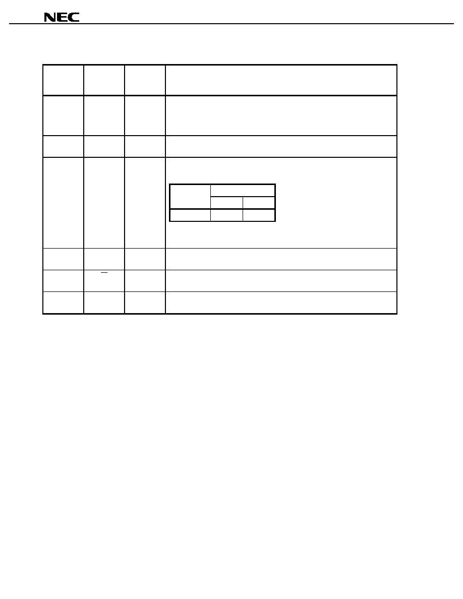
PIN CONNECTIONS
Pin No.
Pin Name
1
OUT
2
GND
3
SW
4
IN
5
IN
6
V
CC
PRODUCT LINE-UP
Part Number
I
CC
(mA)
V
CC
(V)
˜
2
f
in
(MHz)
˜
4
f
in
(MHz)
˜
8
f
in
(MHz)
Package
µ
PB1509 GV
5.0
2.2 to 5.5
50 to 700
50 to 800
50 to 1 000
8-pin SSOP
µ
PB1511TB
3.5
2.4 to 3.3
50 to 700
50 to 800
-
6-pin super minimold
Remark
This table shows the TYP. values of main parameters. Please refer to ELECTRICAL CHARACTERISTICS.
INTERNAL BLOCK DIAGRAM
D
CLK
Q
Q
D
CLK
Q
Q
SW
OUT
IN
IN
(Top View)
3
2
1
4
5
6
(Bottom View)
4
5
6
3
2
1
C2Z

Preliminary Data Sheet P14731EJ1V0DS00
3
µ
µ
µ
µ
PB1511TB
SYSTEM APPLICATION EXAMPLE
One of the example for usage
VCO
I
Q
˜
N
PLL
PA
DEMOD.
PLL
˜
N
PB1511TB
SW
RX
TX
0
∞
I
90
∞
Q
VCO
µ
Low Noise Tr.
Quadulator Modulator
Phase
Shifter
This block diagram schematically shows the
µ
PB1511TB's location in one of the example application system. The
other applications are also acceptable for divider use.
Preliminary Data Sheet P14731EJ1V0DS00
4
µ
µ
µ
µ
PB1511TB
PIN EXPLANATIONS
Pin No.
Symbol
Applied
Voltage
(V)
Functions and Explanation
1
OUT
Divided frequency output pin. This pin is designed as emitter follower output. This
pin can output 0.2 V
P-P
MIN. with 200
load.
This pin should be coupled to load device with capacitor (example: 1 000 pF) for
DC cut.
2
GND
0
Ground pin. Ground pattern on the board should be formed as widely as possible
to minimize ground impedance.
3
SW
H/L
Divide ratio control pin. Divide ratio can be determined by following applied level
to these pins.
These pins must be each equipped with bypass capacitor to minimize their
impedance.
4
IN
Signal input pin. This pin should be coupled to signal source with capacitor
(example: 1 000 pF) for DC cut.
5
IN
Signal input bypass pin. This pin must be equipped with bypass capacitor
(example: 1 000 pF) to minimize ground impedance.
6
V
CC
2.4 to 3.3
Power supply pin. This pin must be equipped with bypass capacitor (example:
1 000 pF) to minimize ground impedance.
SW
H
L
Divide ratio
1/2
1/4
Preliminary Data Sheet P14731EJ1V0DS00
5
µ
µ
µ
µ
PB1511TB
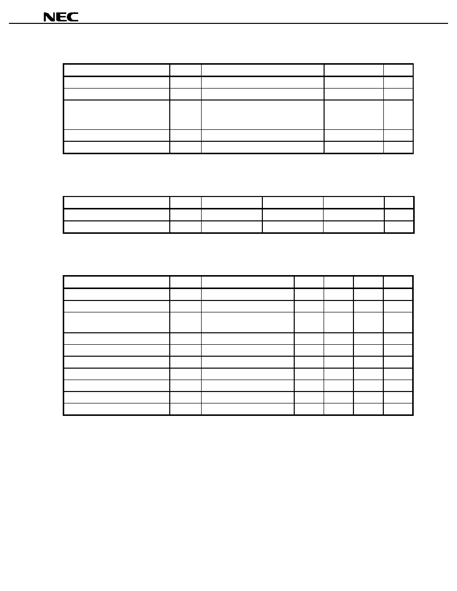
ABSOLUTE MAXIMUM RATINGS
Parameter
Symbol
Conditions
Ratings
Unit
Supply Voltage
V
CC
T
A
= +25
∞
C
3.6
V
Input Voltage
V
in
T
A
= +25
∞
C, SW pin
3.6
V
Total Power Dissipation
P
D
Mounted on double sided copper clad 50
◊
50
◊
1.6 mm epoxy glass PWB (T
A
=
+85
∞
C)
200
mW
Operating Ambient Temperature
T
A
-
40 to +85
∞
C
Storage Temperature
T
stg
-
55 to +150
∞
C
RECOMMENDED OPERATING CONDITIONS
Parameter
Symbol
MIN.
TYP.
MAX.
Unit
Supply Voltage
V
CC
2.4
3.0
3.3
V
Operating Ambient Temperature
T
A
-
40
+25
+85
∞
C
ELECTRICAL CHARACTERISTICS (T
A
= +25
∞
∞
∞
∞
C, V
CC
= 3.0 V)
Parameter
Symbol
Test Conditions
MIN.
TYP.
MAX.
Unit
Circuit Current
I
CC
No signals
3.1
3.5
4.1
mA
Upper Limit Operating Frequency 1
f
in(U)1
P
in
=
-
20 to 0 dBm
500
MHz
Upper Limit Operating Frequency 2
f
in(U)2
P
in
=
-
20 to
-
5 dBm @
˜
2
@
˜
4
700
800
MHz
Lower Limit Operating Frequency 1
f
in(L)1
P
in
=
-
20 to 0 dBm
50
MHz
Lower Limit Operating Frequency 2
f
in(L)2
P
in
=
-
20 to
-
5 dBm
500
MHz
Input Power 1
P
in1
f
in
= 50 to 800 MHz
-
20
-
5
dBm
Input Power 2
P
in2
f
in
= 50 to 500 MHz
-
20
0
dBm
Output Voltage
V
out
R
L
= 200
0.2
0.3
V
P-P
Divide Ratio Control Input High
V
IH
0.7
◊
V
CC
V
CC
+ 0.5
V
Divide Ratio Control Input Low
V
IL
-
0.5
V
CC
◊
0.3
V