 | –≠–ª–µ–∫—Ç—Ä–æ–Ω–Ω—ã–π –∫–æ–º–ø–æ–Ω–µ–Ω—Ç: 2SC5180 | –°–∫–∞—á–∞—Ç—å:  PDF PDF  ZIP ZIP |
©
1994
DATA SHEET
SILICON TRANSISTOR
2SC5180
FEATURES
∑
Low current consumption and high gain
S
21e
2
= 12 dB TYP. @ V
CE
= 2 V, I
C
= 7 mA, f = 2 GHz
S
21e
2
= 11 dB TYP. @ V
CE
= 1 V, I
C
= 5 mA, f = 2 GHz
∑
Supper Mini-Mold package
ORDERING INFORMATION
PART
QUANTITY
ARRANGEMENT
NUMBER
Embossed tape, 8 mm wide, pins No. 3
2SC5180≠T1
(base) and No. 4 (emitter) facing the
3 000 units/reel
perforations
Embossed tape, 8 mm wide, pins No. 1
2SC5180≠T2
(collector) and No. 2 (emitter) facing the
perforations
* Contact your NEC sales representatives to order samples for evaluation (available
in batches of 50).
ABSOLUTE MAXIMUM RATINGS (T
A
= 25
∞
C)
Collector to Base Voltage
V
CBO
5
V
Collector to Emitter Voltage
V
CEO
3
V
Emitter to Base Voltage
V
EBO
2
V
Collector Current
I
C
10
mA
Total Power Dissipation
P
T
30
mW
Junction Temperature
T
j
150
∞
C
Storage Temperature
T
stg
≠65 to +150
∞
C
2.0 ± 0.2
1.25 ± 0.1
2
1
3
4
(1.25)
0.65
0.60
0.3
+0.1
≠0.05
0.4
+0.1
≠0.05
0.3
+0.1
≠0.05
0.3
+0.1
≠0.05
(1.3)
0.9 ± 0.1
0.3
0.15
+0.1
≠0.05
0 to 0.1
2.1 ± 0.2
T84
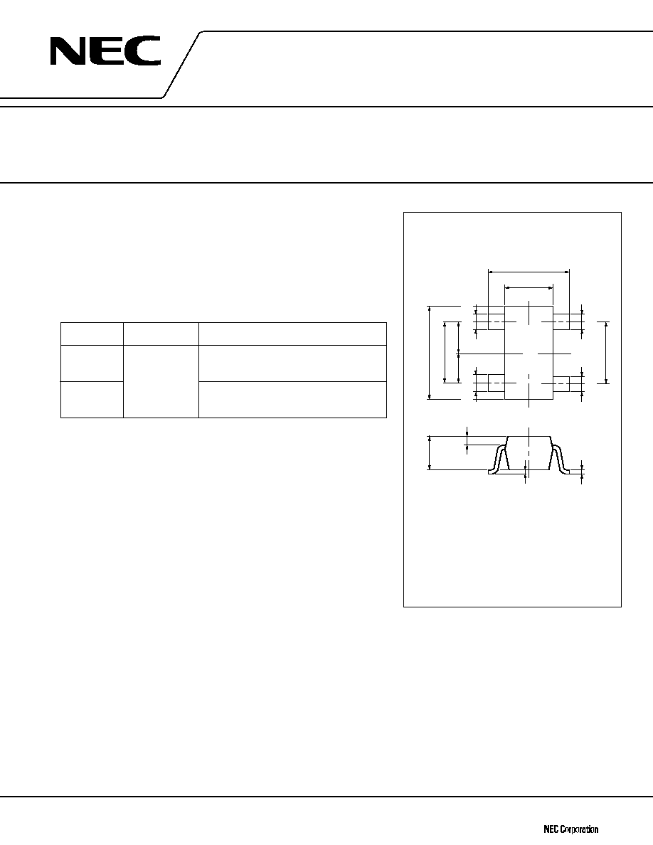
PACKAGE DIMENSIONS
(Units : mm)
1. Collector
2. Emitter
3. Base
4. Emitter
PIN CONNECTIONS
NPN EPITAXIAL SILICON TRANSISTOR IN SUPER MINI-MOLD PACKAGE
FOR LOW-NOISE MICROWAVE AMPLIFICATION
Caution;
This transistor uses high-frequency technology. Be careful not to allow excessive current to flow through the transistor, including static electricity.
Document No. P12104EJ2V0DS00 (2nd edition)
(Previous No. TC-2477)
Date Published December 1996 N
Printed in Japan

2
2SC5180
ELECTRICAL CHARACTERISTICS (T
A
= 25
∞
C)
PARAMETER
SYMBOL
MIN.
TYP.
MAX.
UNIT
CONDITIONS
Collector Cutoff Current
I
CBO
100
nA
V
CB
= 5 V, I
E
= 0
Emitter Cutoff Current
I
EBO
100
nA
V
EB
= 1 V, I
C
= 0
DC Current Gain
h
FE
70
140
V
CE
= 2 V, I
C
= 7 mA*
1
Insertion Power Gain (1)
S
21e
2
10
12
dB
V
CE
= 2 V, I
C
= 7 mA, f = 2 GHz
Insertion Power Gain (2)
S
21e
2
8.5
11
dB
V
CE
= 1 V, I
C
= 5 mA, f = 2 GHz
Noise Figure (1)
NF
1.5
2.0
dB
V
CE
= 2 V, I
C
= 3 mA, f = 2 GHz
Noise Figure (2)
NF
1.5
2.0
dB
V
CE
= 1 V, I
C
= 3 mA, f = 2 GHz
Gain Bandwidth Product (1)
f
T
12
15.5
GHz
V
CE
= 2 V, I
C
= 7 mA, f = 2 GHz
Gain Bandwidth Product (2)
f
T
10
13
GHz
V
CE
= 1 V, I
C
= 5 mA, f = 2 GHz
Feedback Capacitance
C
re
0.3
0.5
pF
V
CB
= 2 V, I
E
= 0 mA, f = 1 MHz*
2
* 1 : Measured with pulses : Pulse width =
< 350
µ
s, duty cycle =
< 2 %, pulsed
* 2 : Measured with a three-terminal bridge. The emitter and case terminal are connected to the guard terminal of the bridge.
h
FE
class
Class
FB
Marking
T84
h
FE
70 to 140

3
2SC5180
CHARACTERISTICS CURVES (T
A
= 25
∞
C)
25
0
20
15
10
5
1.0
2.0
3.0
COLLECTOR CURRENT vs.
COLLECTOR TO EMITTER VOLTAGE
I
C
≠ Collector Current ≠ mA
V
CE
≠ Collector to Emitter Voltage ≠ V
TOTAL POWER DISSIPATION
vs. AMBIENT TEMPERATURE
COLLECTOR CURRENT vs.
BASE TO EMITTER VOLTAGE
0
50
200
100
0
50
100
150
40
30
20
10
0.5
1.0
T
A
≠ Ambient Temperature ≠ ∞C
V
BE
≠ Base to Emitter Voltage ≠ V
P
T
≠ Total Power Dissipation ≠ mW
I
C
≠ Collector Current ≠ mA
V
CE
= 2 V
30 mW
I
B
= 20 A
µ
40 A
µ
60 A
µ
80 A
µ
100 A
µ
120 A
µ
140 A
µ
160 A
µ
180 A
µ
200 A
µ
Passive
air cooling
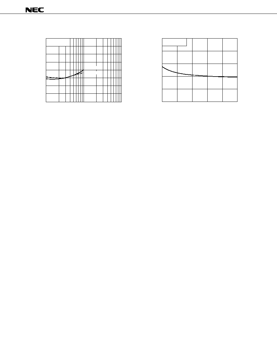
GAIN BAND WIDTH PRODUCT
vs. COLLECTOR CURRENT
INSERTION POWER GAIN
vs. COLLECTOR CURRENT
1
14
18
1
2
5
10
12
10
8
6
2
10
I
C
≠ Collector Current ≠ mA
I
C
≠ Collector Current ≠ mA
f
T
≠ Gain Bandwidth Product ≠ GHz
16
14
12
10
8
6
4
f = 2 GHz
4
5
S
21e
2
≠ Insertion Power Gain ≠ dB
V
CE
= 2 V
V
CE
= 1 V
f = 2 GHz
2 V
V
CE
= 1 V
I
C
≠ Collector Current ≠ mA
h
FE
≠ DC Current Gain
DC CURRENT GAIN vs.
COLLECTOR CURRENT
500
200
100
10
20
50
1
2
5
10
20
50
100
V
CE
= 1 V
V
CE
= 2 V
4
2SC5180
0
4
3
2
1
10
20
100
0.1
0.3
0.4
0.5
1.0
2.0
3.0
4.0
FEED-BACK CAPACITANCE vs.
COLLECTOR TO BASE VOLTAGE
NOISE FIGURE vs.
COLLECTOR CURRENT
NF ≠ Noise Figure ≠ dB
I
C
≠ Collector Current ≠ mA
C
re
≠ Feedback Capacitance ≠ pF
V
CB
≠ Collector to Base Voltage ≠ V
5.0
0.2
1
2
5
V
CE
= 1 V
V
CE
= 2 V
f = 2 GHz
f = 1 MHz
0

5
2SC5180
S≠PARAMETER
V
CE
= 1 V, I
C
= 1 mA, Z
O
= 50
FREQUENCY
S11
S21
S12
S22
MHz
MAG
ANG
MAG
ANG
MAG
ANG
MAG
ANG
600.00
0.916
≠28.0
3.247
147.1
0.074
65.6
0.960
≠21.2
800.00
0.816
≠36.9
3.092
136.2
0.111
58.6
0.887
≠26.2
1000.00
0.741
≠47.1
2.929
125.5
0.140
54.4
0.810
≠32.8
1200.00
0.691
≠55.8
2.864
116.5
0.158
52.2
0.788
≠39.3
1400.00
0.628
≠63.3
2.762
109.6
0.179
48.2
0.744
≠44.5
1600.00
0.558
≠72.3
2.590
100.9
0.195
44.8
0.692
≠49.2
1800.00
0.508
≠80.9
2.505
93.4
0.199
43.7
0.647
≠54.7
2000.00
0.444
≠87.8
2.293
88.1
0.196
39.5
0.602
≠58.2
2200.00
0.386
≠94.3
2.111
81.8
0.201
35.8
0.575
≠61.2
V
CE
= 1 V, I
C
= 3 mA, Z
O
= 50
FREQUENCY
S11
S21
S12
S22
MHz
MAG
ANG
MAG
ANG
MAG
ANG
MAG
ANG
600.00
0.694
≠43.6
6.614
129.7
0.063
57.9
0.819
≠30.4
800.00
0.557
≠54.5
5.730
117.1
0.090
54.4
0.707
≠35.6
1000.00
0.463
≠63.1
5.054
106.4
0.113
52.6
0.609
≠41.1
1200.00
0.394
≠70.7
4.628
99.0
0.125
54.2
0.575
≠45.5
1400.00
0.325
≠78.9
4.123
92.2
0.143
52.5
0.526
≠48.8
1600.00
0.269
≠88.2
3.744
84.3
0.157
51.5
0.478
≠52.5
1800.00
0.226
≠96.9
3.488
79.4
0.160
52.5
0.441
≠57.0
2000.00
0.181
≠103.5
3.085
75.5
0.166
50.8
0.412
≠57.9
2200.00
0.146
≠111.9
2.776
70.5
0.174
48.1
0.401
≠60.0
V
CE
= 1 V, I
C
= 5 mA, Z
O
= 50
FREQUENCY
S11
S21
S12
S22
MHz
MAG
ANG
MAG
ANG
MAG
ANG
MAG
ANG
600.00
0.556
≠51.5
7.925
120.8
0.055
57.5
0.729
≠33.5
800.00
0.430
≠61.6
6.573
108.7
0.083
55.0
0.614
≠37.4
1000.00
0.338
≠68.2
5.644
98.8
0.102
54.0
0.527
≠41.0
1200.00
0.271
≠75.3
5.047
92.4
0.117
57.7
0.498
≠44.6
1400.00
0.217
≠84.1
4.409
86.0
0.133
56.5
0.451
≠47.5
1600.00
0.171
≠94.6
3.985
78.8
0.148
55.9
0.414
≠50.0
1800.00
0.137
≠104.4
3.674
74.9
0.155
57.4
0.382
≠53.9
2000.00
0.100
≠114.7
3.229
71.4
0.162
55.7
0.361
≠55.0
2200.00
0.079
≠125.3
2.897
66.9
0.173
53.0
0.357
≠57.2
V
CE
= 1 V, I
C
= 7 mA, Z
O
= 50
FREQUENCY
S11
S21
S12
S22
MHz
MAG
ANG
MAG
ANG
MAG
ANG
MAG
ANG
600.00
0.455
≠57.2
8.518
114.4
0.051
56.0
0.657
≠34.1
800.00
0.335
≠67.4
6.873
103.1
0.075
55.1
0.557
≠36.6
1000.00
0.252
≠73.2
5.825
93.9
0.095
56.7
0.480
≠39.2
1200.00
0.194
≠80.5
5.131
88.3
0.113
59.7
0.453
≠41.8
1400.00
0.148
≠91.1
4.447
82.0
0.129
58.7
0.417
≠44.6
1600.00
0.114
≠105.9
4.018
75.3
0.145
58.7
0.385
≠46.8
1800.00
0.087
≠119.5
3.682
71.9
0.152
60.6
0.357
≠50.6
2000.00
0.062
≠140.8
3.230
68.6
0.161
58.1
0.341
≠51.5
2200.00
0.051
≠160.7
2.893
64.4
0.170
55.7
0.342
≠54.0