 | –≠–ª–µ–∫—Ç—Ä–æ–Ω–Ω—ã–π –∫–æ–º–ø–æ–Ω–µ–Ω—Ç: 2SC5181 | –°–∫–∞—á–∞—Ç—å:  PDF PDF  ZIP ZIP |
SILICON TRANSISTOR
FEATURES
∑
Low current consumption and high gain
|S
21e
|
2
= 10.5 dB
TYP.
@ V
CE
= 2 V, I
C
= 7 mA, f = 2 GHz
|S
21e
|
2
= 9.0 dB
TYP.
@V
CE
= 1 V, I
C
= 5 mA, f = 2 GHz
∑
Ultra Super Mini-Mold package
ORDERING INFORMATION
PART
QUANTITY
ARRANGEMENT
NUMBER
2SC5181
50 units/box
2SC5181-T1
3 000 units/reel
*
Contact your NEC sales representatives to order samples for
evaluation (available in batches of 50).
ABSOLUTE MAXIMUM RATINGS (T
A
= 25
∞
C)
Collector to Base Voltage
V
CBO
5
V
Collector to Emitter Voltage
V
CEO
3
V
Emitter to Base Voltage
V
EBO
2
V
Collector Current
I
C
10
mA
Total Power Dissipation
P
T
30
mW
Junction Temperature
T
j
150
∞
C
Storage Temperature
T
stg
≠65 to +150
∞
C
2SC5181
Document No. P12105EJ2V0DS00 (2nd edition)
(Previous No. TC-2478)
Date Published November 1996 N
Printed in Japan
©
1994
DATA SHEET
NPN EPITAXIAL SILICON TRANSISTOR IN ULTRA SUPER MINI-MOLD PACKAGE
FOR LOW-NOISE MICROWAVE AMPLIFICATION
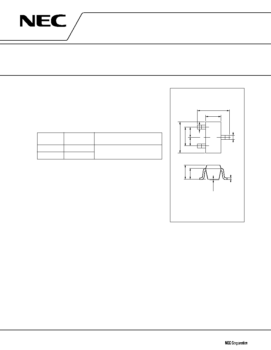
1.6 ± 0.1
0.8 ± 0.1
3
2
1
1.6 ± 0.1
1.0
0.5
0.5
0.75 ± 0.05
0.6
0.15
≠0.05
+0.1
0.3
≠0
+0.1
0.2
≠0
+0.1
0 to 0.1
84
PIN CONNECTIONS
1. Emitter
2. Base
3. Collector
PACKAGE DIMENSIONS
(Units: mm)
Embossed tape, 8 mm wide, pin No. 3
(collector) facing the perforation
Caution; This transistor uses high-frequency technology. Be careful not to allow excessive current to flow through the transistor, including static electricity.
2SC5181
2
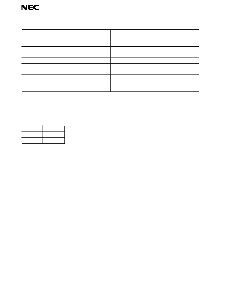
ELECTRICAL CHARACTERISTICS (T
A
= 25
∞
C)
PARAMETER
SYMBOL
MIN.
TYP.
MAX.
UNIT
CONDITIONS
Collector Cutoff Current
I
CBO
100
nA
V
CB
= 5 V, I
E
= 0
Emitter Cutoff Current
I
EBO
100
nA
V
EB
= 1 V, I
C
= 0
DC Current Gain
h
FE
70
140
V
CE
= 2 V, I
C
= 7 mA
*1
Insertion Power Gain (1)
|S
21e
|
2
8.0
10.5
dB
V
CE
= 2 V, I
C
= 7 mA, f = 2 GHz
Insertion Power Gain (2)
|S
21e
|
2
7.0
9.0
dB
V
CE
= 1 V, I
C
= 5 mA, f = 2 GHz
Noise Figure (1)
NF
1.5
2.0
dB
V
CE
= 2 V, I
C
= 3 mA, f = 2 GHz
Noise Figure (2)
NF
1.5
2.0
dB
V
CE
= 1 V, I
C
= 3 mA, f = 2 GHz
Gain Bandwidth Product (1)
f
T
10
13
GHz
V
CE
= 2 V, I
C
= 7 mA, f = 2 GHz
Gain Bandwidth Product (2)
f
T
8.5
12
GHz
V
CE
= 1 V, I
C
= 5 mA, f = 2 GHz
Feedback Capacitance
C
re
0.4
0.6
pF
V
CB
= 2 V, I
E
= 0 mA, f = 1 MHz
*2
*1.
Measured with pulses: Pulse width
350
µ
s, duty cycle
2 %, pulsed
*2.
Measured with a three-terminal bridge. The emitter and case terminal are connected to the guard terminal
of the bridge.
h
FE
Class
Class
FB
Marking
84
h
FE
70 to 140
2SC5181
3
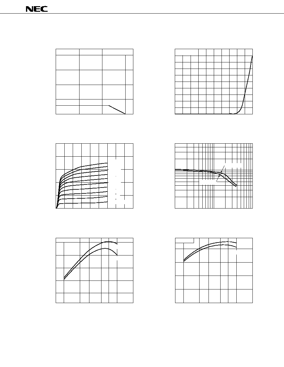
CHARACTERISTICS CURVES (T
A
= 25
∞
C)
TOTAL POWER DISSIPATION vs.
AMBIENT TEMPERATURE
T
A
≠ Ambient Temperature ≠ ∞C
P
T
≠ Total Power Dissipation ≠ mW
0
COLLECTOR CURRENT vs.
BASE TO EMITTER VOLTAGE
V
BE
≠ Base to Emitter Voltage ≠ V
I
C
≠ Collector Current ≠ mA
0
COLLECTOR CURRENT vs.
COLLECTOR TO EMITTER
V
CE
≠ Collector to Emitter Voltage ≠ V
I
C
≠ Collector Current ≠ mA
0
V
CE
= 2 V
50
30 mW
100
200
100
150
0.5
1.0
10
20
30
40
50
20
15
10
5
25
1.0
2.0
3.0
200 A
180 A
160 A
140 A
120 A
100 A
80 A
60 A
40 A
I
B
= 20 A
Passive air cooling
µ
µ
µ
µ
µ
µ
µ
µ
µ
µ
GAIN BANDWIDTH PRODUCT vs.
COLLECTOR CURRENT
INSERTION POWER GAIN vs.
COLLECTOR CURRENT
I
C
≠ Collector Current ≠ mA
f
T
≠ Gain Bandwidth Product ≠ GHz
1
I
C
≠ Collector Current ≠ mA
|S
21e
|
2
≠ Insertion Power Gain ≠ dB
0
1
2
3
5
7
10
20
5
10
5
10
15
f = 2 GHz
f = 2 GHz
2
3
5
7
10
20
V
CE
= 2 V
V
CE
= 1 V
V
CE
= 2 V
V
CE
= 1 V
I
C
≠ Collector Current ≠ mA
h
FE
≠ DC Current Gain
DC CURRENT GAIN vs.
COLLECTOR CURRENT
500
200
100
10
20
50
1
2
5
10
20
50
100
V
CE
= 1 V
V
CE
= 2 V

2SC5181
4
NOISE FIGURE vs.
COLLECTOR CURRENT
I
C
≠ Collector Current ≠ mA
NF ≠ Noise Figure ≠ dB
FEED-BACK CAPACITANCE vs.
COLLECTOR TO BASE VOLTAGE
2
1
1
2
3
7
10
5
3
20
V
CB
≠ Collector to Base Voltage ≠ V
C
re
≠ Feedback Capacitance ≠ pF
0.0
2.0
4.0
6.0
8.0
10.0
0.2
0.4
0.6
0.8
f = 1 MHz
f = 2 GHz
V
CE
= 1 V
V
CE
= 2 V

2SC5181
5
S-PARAMETERS
V
CE
= 1 V, I
C
= 1 mA, Z
O
= 50
FREQUENCY
S11
S21
S12
S22
MHz
600.00
800.00
1000.00
1200.00
1400.00
1600.00
1800.00
2000.00
2200.00
ANG
≠25.9
≠32.1
≠39.9
≠47.4
≠53.1
≠58.2
≠64.2
≠68.9
≠74.6
ANG
≠31.5
≠40.9
≠50.9
≠60.1
≠66.6
≠73.7
≠80.6
≠88.8
≠97.7
MAG
0.934
0.847
0.759
0.726
0.688
0.636
0.575
0.530
0.495
ANG
64.7
58.9
53.0
49.8
45.9
42.5
41.3
39.6
35.7
MAG
3.159
2.964
2.762
2.674
2.590
2.409
2.285
2.182
2.032
MAG
0.113
0.152
0.180
0.204
0.228
0.253
0.265
0.270
0.278
MAG
0.892
0.795
0.704
0.653
0.598
0.524
0.464
0.415
0.355
ANG
142.3
130.8
119.7
110.1
103.0
94.9
87.2
81.7
74.6
V
CE
= 1 V, I
C
= 3 mA, Z
O
= 50
FREQUENCY
S11
S21
S12
S22
MHz
600.00
800.00
1000.00
1200.00
1400.00
1600.00
1800.00
2000.00
2200.00
ANG
≠37.3
≠43.1
≠49.5
≠54.2
≠57.6
≠61.1
≠66.7
≠69.5
≠75.0
ANG
≠48.4
≠59.5
≠68.5
≠76.1
≠81.4
≠88.0
≠92.7
≠105.8
≠121.6
MAG
0.754
0.629
0.533
0.493
0.448
0.411
0.369
0.334
0.311
ANG
59.6
55.7
53.0
53.5
51.6
50.1
49.7
50.0
46.8
MAG
6.121
5.199
4.502
4.084
3.661
3.279
3.024
2.796
2.535
MAG
0.095
0.123
0.143
0.165
0.183
0.204
0.220
0.230
0.244
MAG
0.653
0.517
0.422
0.362
0.301
0.245
0.209
0.175
0.132
ANG
124.0
111.4
100.6
92.8
86.8
79.5
74.1
70.4
64.5
FREQUENCY
S11
S21
S12
S22
MHz
600.00
800.00
1000.00
1200.00
1400.00
1600.00
1800.00
2000.00
2200.00
ANG
≠40.3
≠44.6
≠48.9
≠52.5
≠55.2
≠58.4
≠63.6
≠65.6
≠71.7
ANG
≠56.3
≠66.9
≠73.5
≠79.7
≠85.5
≠91.8
≠96.2
≠116.1
≠142.5
MAG
0.648
0.530
0.446
0.414
0.379
0.347
0.313
0.283
0.268
ANG
57.8
57.0
56.4
56.4
55.2
53.8
53.5
53.3
50.7
MAG
7.156
5.830
4.939
4.391
3.865
3.440
3.155
2.900
2.614
MAG
0.082
0.109
0.131
0.151
0.175
0.196
0.213
0.227
0.241
MAG
0.514
0.389
0.307
0.253
0.202
0.157
0.130
0.108
0.077
ANG
115.3
103.5
93.6
86.9
81.4
74.7
70.1
67.0
61.5
V
CE
= 1 V, I
C
= 7 mA, Z
O
= 50
FREQUENCY
S11
S21
S12
S22
MHz
600.00
800.00
1000.00
1200.00
1400.00
1600.00
1800.00
2000.00
2200.00
ANG
≠40.5
≠43.6
≠46.6
≠49.4
≠51.8
≠54.5
≠59.5
≠61.4
≠67.2
ANG
≠61.9
≠72.5
≠78.2
≠84.9
≠91.4
≠98.8
≠104.3
≠136.6
≠174.6
MAG
0.570
0.469
0.399
0.374
0.347
0.322
0.290
0.264
0.249
ANG
59.1
59.0
57.9
59.2
57.6
56.2
55.3
55.9
52.7
MAG
7.590
6.043
5.059
4.454
3.886
3.455
3.162
2.898
2.606
MAG
0.077
0.101
0.124
0.145
0.169
0.191
0.210
0.224
0.237
MAG
0.405
0.305
0.229
0.184
0.141
0.106
0.086
0.071
0.060
ANG
109.4
98.4
89.2
83.2
78.0
71.6
67.6
64.6
59.4
V
CE
= 1 V, I
C
= 3 mA, Z
O
= 50