PLEASE NOTE:
PLEASE NOTE:
PLEASE NOTE:
PLEASE NOTE:
PLEASE NOTE:
The following part numbers
The following part numbers
The following part numbers
The following part numbers
The following part numbers
from this datasheet are not
from this datasheet are not
from this datasheet are not
from this datasheet are not
from this datasheet are not
recommended for new design.
recommended for new design.
recommended for new design.
recommended for new design.
recommended for new design.
Please call sales office for
Please call sales office for
Please call sales office for
Please call sales office for
Please call sales office for
details:
details:
details:
details:
details:
NE68730
NE68730
NE68730
NE68730
NE68730
NE68733
NE68733
NE68733
NE68733
NE68733
NE68739
NE68739
NE68739
NE68739
NE68739
NE68739R
NE68739R
NE68739R
NE68739R
NE68739R
PART NUMBER
1
NE68718
NE68719
NE68730
NE68733
NE68739/39R
EIAJ
2
REGISTERED NUMBER
2SC5185
2SC5186
2SC5184
2SC5182
2SC5183/83R
PACKAGE OUTLINE
18
19
30
33
39/39R
SYMBOLS
PARAMETERS AND CONDITIONS UNITS MIN TYP MAX MIN TYP MAX MIN TYP MAX MIN TYP MAX MIN TYP MAX
f
T
Gain Bandwidth Product at
V
CE
= 2 V, I
C
= 20 mA, f = 2.0 GHz
GHz
10
13
9
11
9
11
9
12
7.5
10
f
T
Gain Bandwidth Product at
V
CE
= 1 V, I
C
= 10 mA, f = 2.0 GHz
GHz
8
11
7
9
7
9
7
10
7
8.5
NF
MIN
Minimum Noise Figure at
V
CE
= 2 V, I
C
= 3 mA, f = 2.0 GHz
dB
1.3
2.0
1.3
2.0
1.3
2.0
1.3
2.0
1.3
2.0
NF
MIN
Minimum Noise Figure at
V
CE
= 1 V, I
C
= 3 mA, f = 2.0 GHz
dB
1.3
2.0
1.3
2.0
1.3
2.0
1.3
2.0
1.3
2.0
|S
21e
|
2
Insertion Power Gain at
V
CE
= 2V, I
C
=20 mA, f = 2.0 GHz
dB
8
11
8.5
10
7
8.5
7
8.5
7.5
10
|S
21e
|
2
Insertion Power Gain at
V
CE
= 1V, I
C
=10 mA, f = 2.0 GHz
dB
7.5
9
6
7.5
6
7.5
6
7.5
7
8.5
h
FE
Forward Current Gain
3
at
V
CE
= 2 V, I
C
= 20 mA
70
140
70
140
70
140
70
140
70
140
I
CBO
Collector Cutoff Current
at V
CB
= 5 V, I
E
= 0 mA
nA
100
100
100
100
100
I
EBO
Emitter Cutoff Current
at V
EB
= 1 V, I
C
= 0 mA
nA
100
100
100
100
100
C
RE4
Feedback Capacitance at
V
CB
= 2 V, I
E
= 0 mA, f = 1 MHz
pF
0.3
0.6
0.4
0.8
0.4
0.8
0.4
0.8
0.4
0.8
P
T
Total Power Dissipation
mW
90
90
90
90
90
R
TH(J-A)
Thermal Resistance
(Junction to Ambient)
∞
C/W
833
1250
833
625
625
R
TH(J-C)
Thermal Resistance
(Junction to Case)
∞
C/W
SURFACE MOUNT NPN SILICON
HIGH FREQUENCY TRANSISTOR
NE687
SERIES
FEATURES
30 (SOT 323 STYLE)
18 (SOT 343 STYLE)
39 (SOT 143 STYLE)
33 (SOT 23 STYLE)
19 (3 PIN ULTRA SUPER
MINI MOLD)
39R (SOT 143R STYLE)
DESCRIPTION
The NE687 series of NPN epitaxial silicon transistors are
designed for low cost, low noise applications. Excellent perfor-
mance at low voltage/low current makes this series an ideal
choice for portable wireless applications at 1.6, 1.9 and 2.4
GHz. The NE687 die is available in six different low cost plastic
surface mount package styles.
ELECTRICAL CHARACTERISTICS
(T
A
= 25
∞
C)
∑ LOW NOISE: 1.3 dB AT 2.0 GHz
∑ LOW VOLTAGE OPERATION
∑ EASY TO MATCH
∑ HIGH GAIN BANDWIDTH PRODUCT: f
T
of 13 GHz
∑ AVAILABLE IN SIX LOW COST PLASTIC SURFACE
MOUNT PACKAGE STYLES
Notes:
1. Precaution: Devices are ESD sensitive. Use proper handling procedures.
2. Electronic Industrial Association of Japan.
California Eastern Laboratories
3. Pulsed measurement, PW
350
µ
s, duty cycle
2%.
4. The emitter terminal should be connected to the ground terminal
of the 3 terminal capacitance bridge.
FREQ.
NF
OPT
G
A
OPT
(MHz)
(dB)
(dB)
MAG
ANG
Rn/50
V
CE =
1.0
V
,
I
C =
3.0 mA
500
1.10
17.66
0.47
15
0.28
800
1.19
14.48
0.39
33
1.20
1000
1.25
12.93
0.34
45
0.28
1500
1.36
9.61
0.29
57
0.27
2000
1.50
7.52
0.24
73
0.27
V
CE =
2.0
V
,
I
C =
3.0 mA
500
1.10
18.60
0.40
12
0.30
800
1.19
15.10
0.35
24
0.22
1000
1.25
13.40
0.31
33
0.26
1500
1.36
10.30
0.26
44
0.28
2000
1.50
8.10
0.23
58
0.28
V
CE =
2.0
V
,
I
C =
20.0
mA
500
2.00
20.30
0.02
-170
0.23
800
2.06
16.70
0.06
171
0.15
1000
2.10
15.00
0.08
172
0.28
1500
2.20
11.90
0.12
178
0.24
2000
2.34
9.80
0.14
-175
0.24
2500
2.46
6.70
0.18
-160
0.23
SYMBOLS
PARAMETERS
UNITS
RATINGS
V
CBO
Collector to Base Voltage
V
5
V
CEO
Collector to Emitter Voltage
V
3
V
EBO
Emitter to Base Voltage
V
2
I
C
Collector Current
mA
30
T
J
Operating Junction
Temperature
∞
C
150
T
STG
Storage Temperature
∞
C
-65 to +150
NE687 SERIES
NE68730
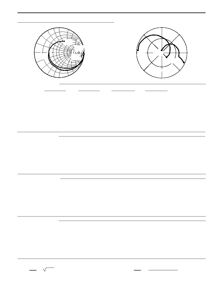
TYPICAL NOISE PARAMETERS
(TA = 25∞C)
NE68739
TYPICAL NOISE PARAMETERS
(T
A
= 25∞C)
FREQ.
NF
OPT
G
A
OPT
(MHz)
(dB)
(dB)
MAG
ANG
Rn/50
V
CE =
0.5
V
,
I
C =
0.5 mA
500
1.23
15.7
0.77
36
0.61
800
1.37
10.9
0.71
46
0.61
1000
1.45
8.7
0.60
64
0.50
V
CE =
1.0
V
,
I
C =
3.0 mA
500
1.07
18.0
0.48
30
0.31
800
1.13
14.8
0.39
49
0.28
1000
1.18
13.2
0.32
60
0.26
1500
1.30
10.5
0.23
76
0.24
2000
1.50
8.0
0.12
120
0.20
2500
1.66
7.0
0.16
-172
0.15
V
CE =
2.0
V
,
I
C =
3.0
mA
500
1.07
18.6
0.46
26
0.28
800
1.13
15.5
0.37
38
0.28
1000
1.18
14.0
0.32
46
0.26
1500
1.30
11.2
0.20
66
0.25
2000
1.50
9.3
0.12
113
0.19
2500
1.66
7.8
0.14
177
0.17
3000
1.86
6.6
0.23
-157
0.10
V
CE =
2.0
V
,
I
C =
20.0
mA
500
1.93
21.2
0.08
-150
0.22
800
1.95
17.6
0.14
-138
0.17
1000
2.00
16.0
0.16
-134
0.17
1500
2.15
12.9
0.21
-127
0.24
2000
2.30
10.6
0.26
-123
0.25
2500
2.40
9.0
0.31
-121
0.25
3000
2.52
7.7
0.46
-114
0.24
ABSOLUTE MAXIMUM RATINGS
1
(T
A
= 25
∞
C)
Note:
1. Operation in excess of any one of these parameters may result
in permanent damage.
V
CE =
0.5
V
,
I
C =
0.5 mA
500
1.10
13.07
0.72
30
1.00
800
1.31
11.23
0.67
54
0.65
1000
1.41
9.36
0.65
67
0.55
V
CE =
1.0 V
,
I
C =
1.0 mA
FREQ.
NF
OPT
G
A
OPT
(MHz)
(dB)
(dB)
MAG
ANG
Rn/50
NE68718
TYPICAL NOISE PARAMETERS
(T
A
= 25∞C)
500
0.93
16.53
0.63
27
0.56
800
1.08
13.44
0.59
47
0.39
1000
1.20
12.21
0.55
62
0.36
1500
1.48
8.53
0.46
83
0.34
2000
1.72
6.50
0.37
107
0.28
500
1.10
18.68
0.48
23
0.28
800
1.15
15.74
0.40
48
0.25
1000
1.20
13.90
0.36
58
0.24
1500
1.38
10.63
0.28
81
0.21
2000
1.60
8.43
0.21
104
0.20
2500
1.82
7.04
0.14
151
0.18
3000
2.00
5.84
0.16
-167
0.13
V
CE =
1.0
V
,
I
C =
3 mA
V
CE =
2
V
,
I
C =
3 mA
V
CE =
2
V
,
I
C =
10 mA
500
1.10
19.83
0.50
21
0.26
800
1.15
16.61
0.42
39
0.26
1000
1.20
14.85
0.38
48
0.25
1500
1.38
11.83
0.29
74
0.24
2000
1.60
9.49
0.23
91
0.22
2500
1.82
8.16
0.14
135
0.20
3000
2.00
6.93
0.13
177
0.12
500
1.60
22.57
0.13
19
0.27
800
1.62
18.75
0.11
48
0.26
1000
1.65
16.91
0.09
67
0.25
1500
1.73
13.52
0.07
100
0.24
2000
1.80
11.17
0.06
143
0.22
2500
2.00
9.48
0.08
-161
0.20
3000
2.19
8.18
0.13
-133
0.16

TYPICAL PERFORMANCE CURVES
(TA = 25
∞
)
NE68719
D.C. POWER DERATING CURVE
Total Power Dissipation, P
T
(mW)
Ambient Temperature, T
A
(
∞
C)
NE68733, NE68739
D.C. POWER DERATING CURVE
Ambient Temperature, T
A
(
∞
C)
Collector Current, I
C
(mA)
Total Power Dissipation, P
T
(mW)
NE68718, NE68730
D.C. POWER DERATING CURVE
150
100
50
0
0
50
100
150
FREE AIR
90
Ambient Temperature, T
A
(
∞
C)
Total Power Dissipation, P
T
(mW)
150
100
90
50
0
0
50
100
150
FREE AIR
200
µ
A
180
µ
A
160
µ
A
140
µ
A
120
µ
A
100
µ
A
80
µ
A
60
µ
A
40
µ
A
I
B
= 20
µ
A
25
20
15
10
5
0
0
2.2
2.4
2.6
COLLECTOR CURRENT vs.
COLLECTOR TO EMITTER VOLTAGE
150
100
90
50
0
0
50
100
150
FREE AIR
Collector to Emitter Voltage, V
CE
(V)
NE687 SERIES

Collector Current, I
C
(mA)
D.C. Current Gain, h
FE
D.C. CURRENT GAIN vs.
COLLECTOR CURRENT
Collector Current, I
C
(mA)
Collector Current, I
C
(mA)
COLLECTOR CURRENT vs.
BASE TO EMITTER VOLTAGE
NE68718
GAIN BANDWIDTH PRODUCT
vs. COLLECTOR CURRENT
NE68730
FEED-BACK CAPACITANCE vs.
COLLECTOR TO BASE VOLTAGE
Insertion Power Gain, |S
21e
|
2
(dB)
Collector Current, I
C
(mA)
NE68718
INSERTION GAIN vs.
COLLECTOR CURRENT
NE68733
NOISE FIGURE vs.
COLLECTOR CURRENT
TYPICAL PERFORMANCE CURVES
(TA = 25
∞
C)
Noise Figure, NF (dB)
Gain Bandwidth Product, f
T
(GHz)
Feed-back Capacitance, C
RE
(pF)
f = 2 GHz
2 V
V
CE
= 1 V
14
12
10
8
4
6
1
2
5
10
20 30
100
V
CE
= 1 V
V
CE
= 2 V
f = 2 GHz
4
3
2
1
0
2
1
5
10
20
100
V
CE
= 1 V
V
CE
= 2 V
500
200
100
50
20
10
1
2
5
10
20
50
100
Collector to Base Voltage, V
CB
(V)
0.6
0.5
0.4
0.3
0.2
1.0
2.0
3.0
4.0
5.0
f = 1 MHz
V
CE
= 2V
50
40
30
20
10
0
0.5
1.0
Base to Emitter Voltage, V
BE
(V)
Collector Current, I
C
(mA)
f = 2 GHz
V
CE
= 1 V
2 V
16
14
12
10
8
6
4
2
1
2
5
10
20 30
100
50
NE687 SERIES