
SILICON TRANSISTOR
2SC5191
MICROWAVE LOW NOISE AMPLIFIER
NPN SILICON EPITAXIAL TRANSISTOR
DATA SHEET
Document No. P10395EJ2V1DS00 (2nd edition)
Date Published March 1997 N
Printed in Japan
1994
©
FEATURES
∑ Low Voltage Operation, Low Phase Distortion
∑ Low Noise
NF = 1.5 dB TYP. @ V
CE
= 3 V, I
C
= 7 mA, f = 2 GHz
NF = 1.7 dB TYP. @ V
CE
= 1 V, I
C
= 3 mA, f = 2 GHz
∑ Large Absolute Maximum Collector Current
I
C
= 100 mA
∑ Mini Mold Package
EIAJ: SC-59
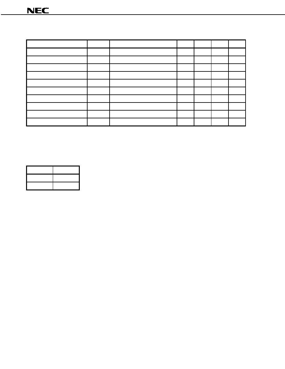
ORDERING INFORMATION
PART
NUMBER
QUANTITY PACKING STYLE
2SC5191-T1 3 Kpcs/Reel Embossed tape 8 mm wide.
Pin 3 (collector) face to perforation side of the tape.
2SC5191-T2 3 Kpcs/Reel Embossed tape 8 mm wide.
Pin 1 (Emitter), Pin 2 (Base) face to perforation side
of the tape.
Remark If you require an evaluation sample, please contact an NEC
Sales Representative. (Unit sample quantity is 50 pcs.)
ABSOLUTE MAXIMUM RATINGS (T
A
= 25
∞
C)
PARAMETER SYMBOL RATING UNIT
Collector to Base Voltage V
CBO
9
V
Collector to Emitter Voltage V
CEO
6
V
Emitter to Base Voltage V
EBO
2
V
Collector Current I
C
100 mA
Total Power Dissipation P
T
200 mW
Junction Temperature T
j
150
∞
C
Storage Temperature T
stg
-
65 to +150
∞
C
This device uses radio frequency technology. Take due precautions to protect it from excessive input levels such as static electricity.
PIN CONNECTIONS
1.
2.
3.
Emitter
Base
Collector
PACKAGE DRAWINGS
(Unit: mm)
2.8±0.2
2.9±0.2
0.65
1.5
3
1
Marking
2
+0.1
-
0.15
0.4
0.95
+0.1
-
0.05
0.16
0 to 0.1
0.3
1.1 to
1.4
+0.1
-
0.06
0.4
+0.1
-
0.05
T88
0.95
2
2SC5191
ELECTRICAL CHARACTERISTICS (T
A
= 25
∞
C)
PARAMETER
SYMBOL
CONDITION
MIN.
TYP.
MAX.
UNIT
Collector Cutoff Current
I
CBO
V
CB
= 5 V, I
E
= 0
100
nA
Emitter Cutoff Current
I
EBO
V
EB
= 1 V, I
C
= 0
100
nA
DC Current Gain
h
FE
V
CE
= 1 V, I
C
= 3 mA
Note 1
80
160
Insertion Power Gain (1)
S
21e
2
V
CE
= 1 V, I
C
= 3 mA, f = 2.0 GHz
2.5
3.5
dB
Insertion Power Gain (2)
S
21e
2
V
CE
= 3 V, I
C
= 20 mA, f = 2.0 GHz
6.5
dB
Noise Figure (1)
NF
V
CE
= 1 V, I
C
= 3 mA, f = 2.0 GHz
1.7
2.5
dB
Noise Figure (2)
NF
V
CE
= 3 V, I
C
= 7 mA, f = 2.0 GHz
1.5
dB
Gain Bandwidth Product (1)
f
T
V
CE
= 1 V, I
C
= 3 mA, f = 2.0 GHz
4
4.5
GHz
Gain Bandwidth Product (2)
f
T
V
CE
= 3 V, I
C
= 20 mA, f = 2.0 GHz
8.5
GHz
Collector Capacitance
C
re
V
CB
= 1 V, I
E
= 0, f = 1.0 MHz
Note 2
0.75
0.85
pF
Notes 1. Pulse Measurement: PW
350
µ
s, Duty cycle
2 %, Pulsed
2. Measured with 3-pin bridge, emitter and case should be connected to guard pin of bridge.
h
FE
Classification
Rank
FB
Marking
T88
h
FE
80 to 160
3
2SC5191
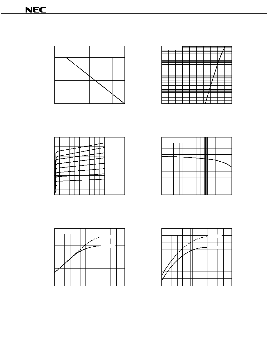
TYPICAL CHARACTERISTICS (T
A
= 25
∞
C)
TOTAL POWER DISSIPATION vs.
AMBIENT TEMPERATURE
Ambient Temperature T
A
(
∞
C)
Free Air
50
100
150
0
100
200
Total Power Dissipation P
T
(mW)
COLLECTOR CURRENT vs.
BASE TO EMITTER VOLTAGE
Base to Emitter Voltage V
BE
(V)
V
CE
= 1 V
0.5
1.0
0
0.01
0.02
0.05
0.1
0.2
0.5
100
20
10
5
2
1
Collector Current I
C
(mA)
COLLECTOR CURRENT vs.
COLLECTOR TO EMITTER VOLTAGE
Collector to Emitter Voltage V
CE
(V)
200 A
180 A
160 A
140 A
120 A
100 A
80 A
60 A
40 A
I
B
= 20 A
µ
µ
µ
µ
µ
µ
µ
µ
µ
µ
1
2
3
4
5
6
0
30
20
10
Collector Current I
C
(mA)
DC CURRENT GAIN vs.
COLLECTOR CURRENT
Collector Current I
C
(mA)
V
CE
= 1 V
1
2
5 10
20
50 100
0.1 0.2
0.5
0
100
200
DC Current Gain h
FE
GAIN BANDWIDTH PRODUCT
vs. COLLECTOR CURRENT
Collector Current I
C
(mA)
f = 2 GHz
1
2
20
5
50
100
10
0
10
8
6
4
2
Gain Bandwidth Product f
T
(GHz)
INSERTION GAIN vs.
COLLECTOR CURRENT
Collector Current I
C
(mA)
f = 2 GHz
1
2
5
10
20
50
100
0
4
2
8
6
Insertion Power Gain |S
21e
|
2
(dB)
V
CE
= 3 V
V
CE
= 1 V
V
CE
= 3 V
V
CE
= 1 V
4
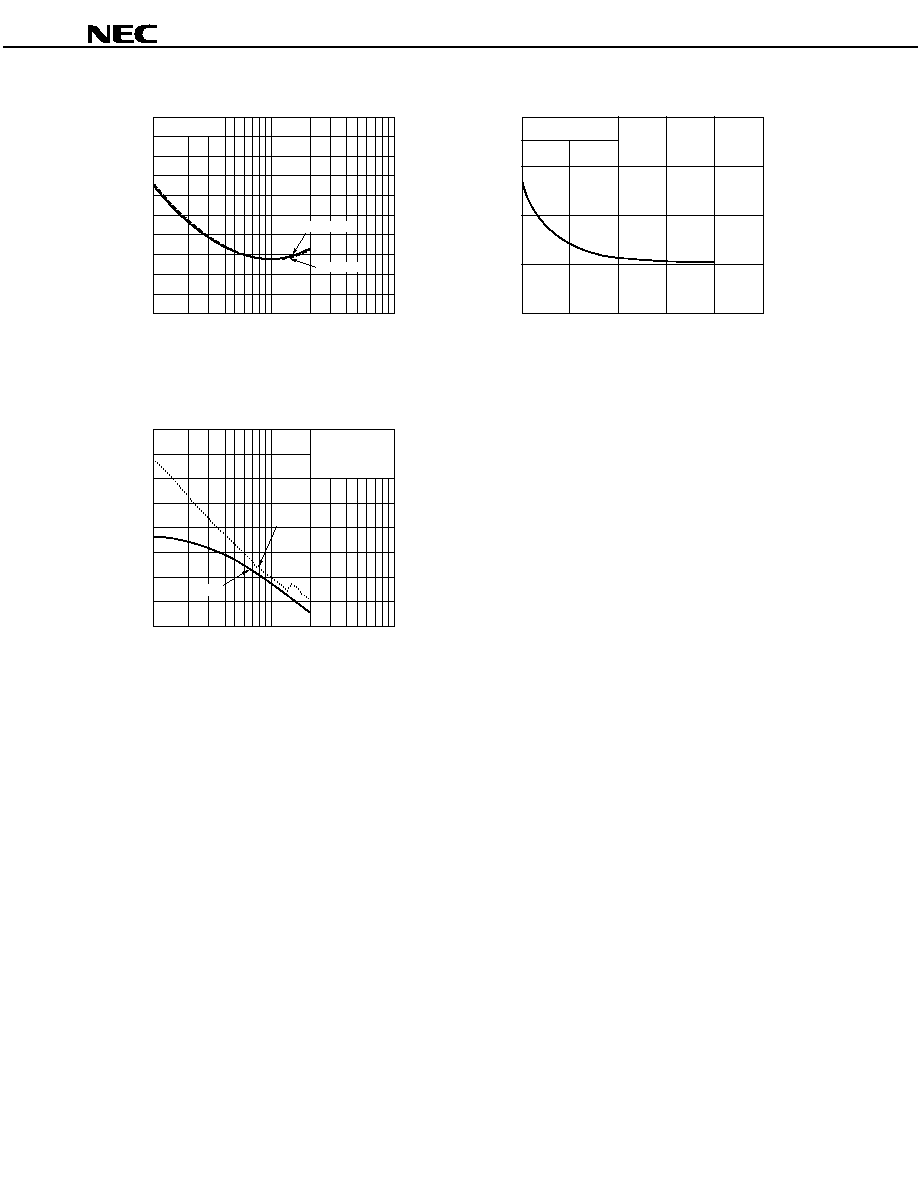
2SC5191
FEED-BACK CAPACITANCE vs.
COLECTOR TO BASE VOLTAGE
Collector to Base Voltage V
CB
(V)
f = 1 MHz
2
4
6
8
10
0
0.4
0.8
0.6
1.2
1.0
Feed-back Capacitance C
re
(pF)
MAXIMUM AVAILABLE GAIN/INSERTION
POWER GAIN vs. FREQUENCY
Frequency f (GHz)
V
CE
= 1 V
I
C
= 3 mA
0.1
0.5
0.2
1
2
5
10
0
20
10
30
40
Maximum Available Power Gain MAG (dB)
Insertion Power Gain |S
21e
|
2
(dB)
NOISE FIGURE vs.
COLLECTOR CURRENT
Collector Current I
C
(mA)
1
2
5
20
10
50
100
3
2
1
0
5
4
Noise Figure NF (dB)
f = 2 GHz
V
CE
= 3 V
MAG
V
CE
= 1 V
|S
21e
|
2
