©
1994
DATA SHEET
SILICON TRANSISTOR
FEATURES
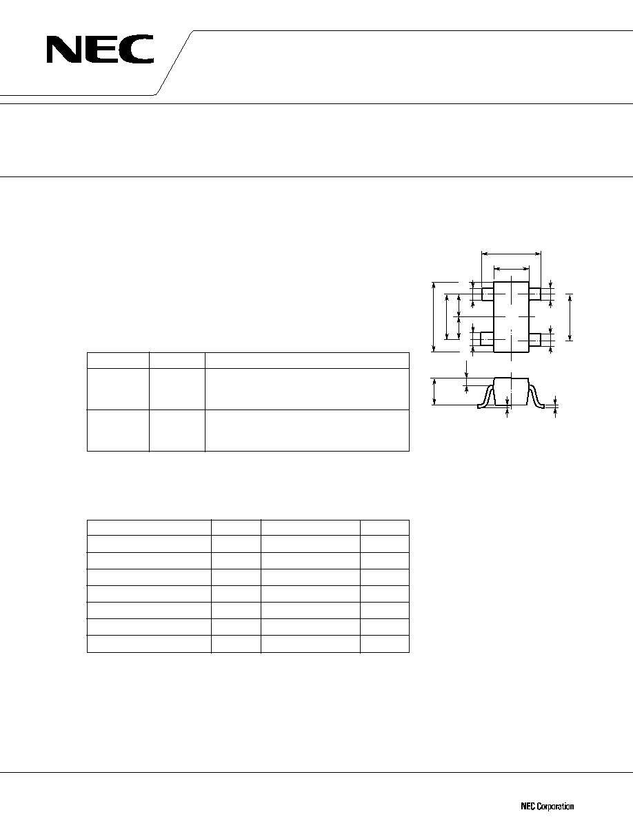
PACKAGE DRAWINGS
∑
Low Voltage Operation, Low Phase Distortion
(Unit: mm)
∑
Low Noise
NF = 1.5 dB TYP. @V
CE
= 3 V, I
C
= 7 mA, f = 2 GHz
NF = 1.7 dB TYP. @V
CE
= 1 V, I
C
= 3 mA, f = 2 GHz
∑
Large Absolute Maximum Collector Current
I
C
= 100 mA
∑
4-Pin Compact Mini Mold Package
ORDERING INFORMATION
PART NUMBER
QUANTITY
PACKING STYLE
2SC5194-T1
3 Kpcs/Reel
Embossed tape 8 mm wide.
Pin 3 (Base), Pin 4 (Emitter) face to perforation
side of the tape.
2SC5194-T2
3 Kpcs/Reel
Embossed tape 8 mm wide.
Pin 1 (Collector), Pin 2 (Emitter) face to
perforation side of the tape.
Remark
If you require an evaluation sample, please contact an NEC
Sales Representative. (Unit sample quantity is 50 pcs.)
ABSOLUTE MAXIMUM RATINGS (T
A
= 25
∞
C)
PARAMETER
SYMBOL
RATING
UNIT
Collector to Base Voltage
V
CBO
9
V
Collector to Emitter Voltage
V
CEO
6
V
Emitter to Base Voltage
V
EBO
2
V
Collector Current
I
C
100
mA
Total Power Dissipation
P
T
150
mW
Junction Temperature
T
j
150
∞C
Storage Temperature
T
stg
≠65 to +150
∞C
2SC5194
This device uses radio frequency technology. Take due precautions to protect it from excessive input levels such as static electricity.
MICROWAVE LOW NOISE AMPLIFIER
NPN SILICON EPITAXIAL TRANSISTOR
2.1±0.2
1.25±0.1
2.0±0.2
0.65
3
T88
PIN CONNECTIONS
1. Collector
2. Emitter
3. Base
4. Emitter
0.60
(1.25)
0.3
≠0.05
+0.1
1
2
+0.1
0.3
≠0.05
+0.1
0.15
≠0.05
+0.1
0.3
0.9±0.1
0 to 0.1
(1.3)
0.3
≠0.05
4
0.4
≠0.05
+0.1
Document No. P10397EJ2V0DS00 (2nd edition)
(Previous No. TD-2487)
Date Published August 1995 P
Printed in Japan
2SC5194
2
ELECTRICAL CHARACTERISTICS (T
A
= 25
∞
C)
PARAMETER
SYMBOL
CONDITION
MIN.
TYP.
MAX.
UNIT
Collector Cutoff Current
I
CBO
V
CB
= 5 V, I
E
= 0
100
nA
Emitter Cutoff Current
I
EBO
V
EB
= 1 V, I
C
= 0
100
nA
DC Current Gain
h
FE
V
CE
= 1 V, I
C
= 3 mA
Note 1
80
160
Insertion Power Gain (1)
|S
21e
|
2
V
CE
= 1 V, I
C
= 3 mA, f = 2.0 GHz
3.0
4.0
dB
Insertion Power Gain (2)
|S
21e
|
2
V
CE
= 3 V, I
C
= 20 mA, f = 2.0 GHz
8.5
dB
Noise Figure (1)
NF
V
CE
= 1 V, I
C
= 3 mA, f = 2.0 GHz
1.7
2.5
dB
Noise Figure (2)
NF
V
CE
= 3 V, I
C
= 7 mA, f = 2.0 GHz
1.5
dB
Gain Bandwidth Product (1)
f
T
V
CE
= 1 V, I
C
= 3 mA, f = 2.0 GHz
4
5
GHz
Gain Bandwidth Product (2)
f
T
V
CE
= 3 V, I
C
= 20 mA, f = 2.0 GHz
10
GHz
Collector Capacitance
C
re
V
CB
= 1 V, I
E
= 0, f = 1.0 MHz
Note 2
0.65
0.8
pF
Notes 1. Pulse Measurement: PW
350
µ
s, Duty cycle
2 %, Pulsed
2. Measured with 3-pin bridge, emitter and case should be connected to guard pin of bridge.
h
FE
Classification
Rank
FB
Marking
T88
h
FE
80 to 160
2SC5194
3
0
50
Ambient Temperature T
A
(∞C)
TOTAL POWER DISSIPATION
vs. AMBIENT TEMPERATURE
Free Air
Total Power Dissipation P
T
(mW)
100
150
100
200
0
1
2
3
4
5
6
Collector to Emitter Voltage V
CE
(V)
COLLECTOR CURRENT vs.
COLLECTOR TO EMITTER VOLTAGE
Collector Current I
C
(mA)
10
20
30
0
0.5
Base to Emitter Voltage V
BE
(V)
COLLECTOR CURRENT vs.
BASE TO EMITTER VOLTAGE
V
CE
= 1 V
Collector Current I
C
(mA)
1
0.01
0.02
0.05
0.1
0.2
0.5
1
2
5
10
20
50
100
0.1
1
0.2
2
20
50
5
0.5
Collector Current I
C
(mA)
DC Current Gain h
FE
10
100
100
0
200
V
CE
= 1 V
DC CURENT GAIN vs.
COLLECTOR CURRENT
200 A
µ
180 A
µ
160 A
µ
140 A
µ
120 A
µ
100 A
µ
80 A
µ
60 A
µ
40 A
µ
I
B
= 20 A
µ
0
1
Collector Current I
C
(mA)
GAIN BANDWIDTH PRODUCT
vs. COLLECTOR CURRENT
V
CE
= 1 V
f = 2 GHz
Gain Bandwidth Product f
T
(GHz)
7
2
3
5
10
1
7
2
3
5
10
5
10
0
5
10
Collector Current I
C
(mA)
INSERTION GAIN vs.
COLLECTOR CURRENT
V
CE
= 1 V
f = 2 GHz
Insertion Power Gain |S
21e
|
2
(dB)
TYPICAL CHARACTERISTICS (T
A
= 25
∞
C)
2SC5194
4
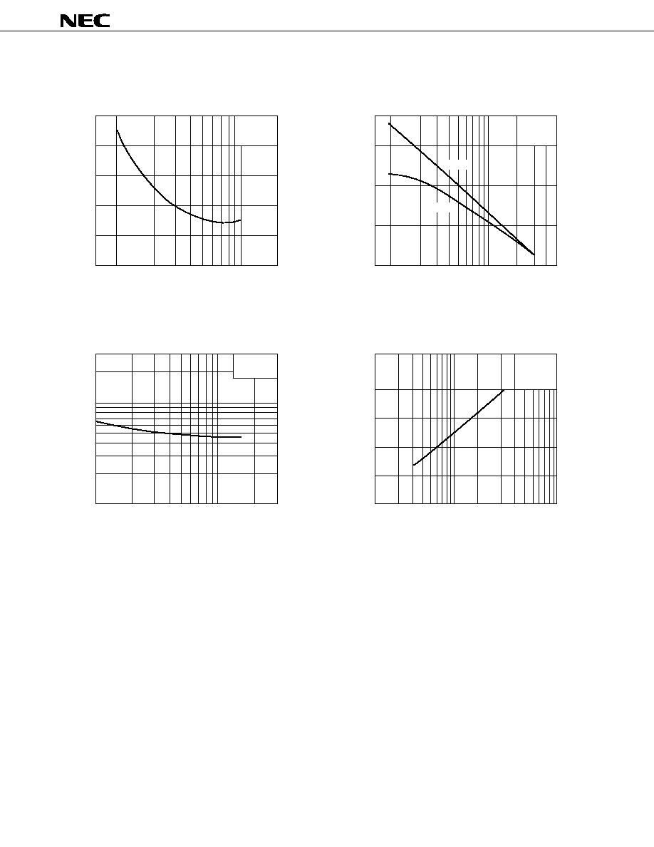
1
Collector Current I
C
(mA)
NOISE FIGURE vs.
COLLECTOR CURRENT
V
CE
= 1 V
f = 2 GHz
Noise Figure NF (dB)
7
20
10
2
3
5
1
2
3
0.1
1
Collector to Base Voltage V
CB
(V)
FEED-BACK CAPACITANCE vs.
COLLECTOR TO BASE VOLTAGE
f = 1 MHz
Feed-back Capacitance C
re
(pF)
20
2
5
10
0.5
1.0
0.5
0.1
Frequency f (GHz)
NOISE FIGURE vs. FREQUENCY
Noise Figure NF (dB)
5
0.5
1
2
1.0
1.5
0
0.1
Frequency f (GHz)
MAXIMUM AVAILABLE GAIN/INSERTION
POWER GAIN vs. FREQUENCY
V
CE
= 1 V
I
C
= 5 mA
V
CE
= 1 V
I
C
= 5 mA
5
0.2
0.5
1
10
20
30
Maximum Available Power Gain MAG (dB)
Insertion Power Gain |S
21e
|
2
(dB)
MAG
|S
21e
|
2
