 | –≠–ª–µ–∫—Ç—Ä–æ–Ω–Ω—ã–π –∫–æ–º–ø–æ–Ω–µ–Ω—Ç: 2SC5195 | –°–∫–∞—á–∞—Ç—å:  PDF PDF  ZIP ZIP |

©
1994
DATA SHEET
SILICON TRANSISTOR
FEATURES
PACKAGE DRAWINGS
∑
Low Voltage Operation, Low Phase Distortion
(Unit: mm)
∑
Low Noise
NF = 1.5 dB TYP. @V
CE
= 3 V, I
C
= 7 mA, f = 2 GHz
NF = 1.5 dB TYP. @V
CE
= 1 V, I
C
= 3 mA, f = 2 GHz
∑
Large Absolute Maximum Collector Current
I
C
= 100 mA
∑
Supercompact Mini Mold Package
ORDERING INFORMATION
PART NUMBER
QUANTITY
PACKING STYLE
2SC5195
In-bulk products
Embossed tape 8 mm wide.
(50 pcs.)
Pin 3 (Collector) face to perforation side of
2SC5195-T1
Taped products
the tape.
(3 Kpcs/Reel)
Remark
If you require an evaluation sample, please contact an NEC
Sales Representative. (Unit sample quantity is 50 pcs.)
ABSOLUTE MAXIMUM RATINGS (T
A
= 25
∞
C)
PARAMETER
SYMBOL
RATING
UNIT
Collector to Base Voltage
V
CBO
9
V
Collector to Emitter Voltage
V
CEO
6
V
Emitter to Base Voltage
V
EBO
2
V
Collector Current
I
C
100
mA
Total Power Dissipation
P
T
125
mW
Junction Temperature
T
j
150
∞C
Storage Temperature
T
stg
≠65 to +150
∞C
2SC5195
MICROWAVE LOW NOISE AMPLIFIER
NPN SILICON EPITAXIAL TRANSISTOR
This device uses radio frequency technology. Take due precautions to protect it from excessive input levels such as static electricity.
1.6±0.1
88
0.15
≠0.05
+0.1
0.6
2
0.75±0.05
1.0
0.5
0.5
1
0.3
≠0
+0.1
3
+0.1
0 to 0.1
PIN CONNECTIONS
1. Emitter
2. Base
3. Collector
0.2
≠0
1.6±0.1
0.8±0.1
Document No. P10398EJ2V0DS00 (2nd edition)
(Previous No. TD-2488)
Date Published August 1995 P
Printed in Japan

2SC5195
2
ELECTRICAL CHARACTERISTICS (T
A
= 25
∞
C)
PARAMETER
SYMBOL
CONDITION
MIN.
TYP.
MAX.
UNIT
Collector Cutoff Current
I
CBO
V
CB
= 5 V, I
E
= 0
100
nA
Emitter Cutoff Current
I
EBO
V
EB
= 1 V, I
C
= 0
100
nA
DC Current Gain
h
FE
V
CE
= 1 V, I
C
= 3 mA
Note 1
80
160
Insertion Power Gain
|S
21e
|
2
V
CE
= 1 V, I
C
= 3 mA, f = 2.0 GHz
3
4
dB
Insertion Power Gain (1)
|S
21e
|
2
V
CE
= 3 V, I
C
= 20 mA, f = 2.0 GHz
8
dB
Noise Figure (2)
NF
V
CE
= 1 V, I
C
= 3 mA, f = 2.0 GHz
1.7
2.5
dB
Noise Figure (1)
NF
V
CE
= 3 V, I
C
= 7 mA, f = 2.0 GHz
1.5
dB
Gain Bandwidth Product (2)
f
T
V
CE
= 1 V, I
C
= 3 mA, f = 2.0 GHz
4.5
5
GHz
Gain Bandwidth Product (1)
f
T
V
CE
= 3 V, I
C
= 20 mA, f = 2.0 GHz
9.5
GHz
Collector Capacitance
C
re
V
CB
= 1 V, I
E
= 0, f = 1.0 MHz
Note 2
0.7
0.8
pF
Notes 1. Pulse Measurement: PW
350
µ
s, Duty cycle
2 %, Pulsed
2. Measured with 3-pin bridge, emitter and case should be connected to guard pin of bridge.
h
FE
Classification
Rank
FB
Marking
88
h
FE
80 to 160
2SC5195
3
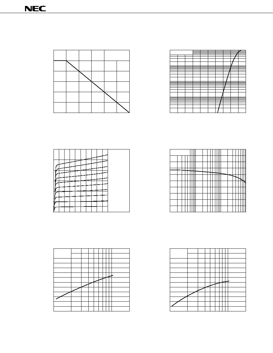
0
50
Ambient Temperature T
A
(∞C)
TOTAL POWER DISSIPATION
vs. AMBIENT TEMPERATURE
Free Air
Total Power Dissipation P
T
(mW)
100
150
50
100
150
0
0.5
Base to Emitter Voltage V
BE
(V)
COLLECTOR CURRENT vs.
BASE TO EMITTER VOLTAGE
V
CE
= 1 V
Collector Current I
C
(mA)
1
0.01
0.1
1
10
100
0.1
1
0.2
2
20
50
5
0.5
Collector Current I
C
(mA)
DC Current Gain h
FE
10
100
100
0
200
V
CE
= 1 V
DC CURENT GAIN vs.
COLLECTOR CURRENT
0
2.5
5
7
Collector to Emitter Voltage V
CE
(V)
COLLECTOR CURRENT vs.
COLLECTOR TO EMITTER VOLTAGE
Collector Current I
C
(mA)
10
20
30
5
15
25
200 A
µ
180 A
µ
160 A
µ
140 A
µ
120 A
µ
100 A
µ
80 A
µ
60 A
µ
40 A
µ
I
B
= 20 A
µ
0
1
Collector Current I
C
(mA)
GAIN BANDWIDTH PRODUCT
vs. COLLECTOR CURRENT
V
CE
= 1 V
f = 2 GHz
Gain Bandwidth Product f
T
(GHz)
7
2
3
5
10
20
5
10
0
1
Collector Current I
C
(mA)
INSERTION GAIN vs.
COLLECTOR CURRENT
V
CE
= 1 V
f = 2 GHz
Insertion Power Gain |S
21e
|
2
(dB)
7
2
3
5
10
20
5
10
TYPICAL CHARACTERISTICS (T
A
= 25
∞
C)
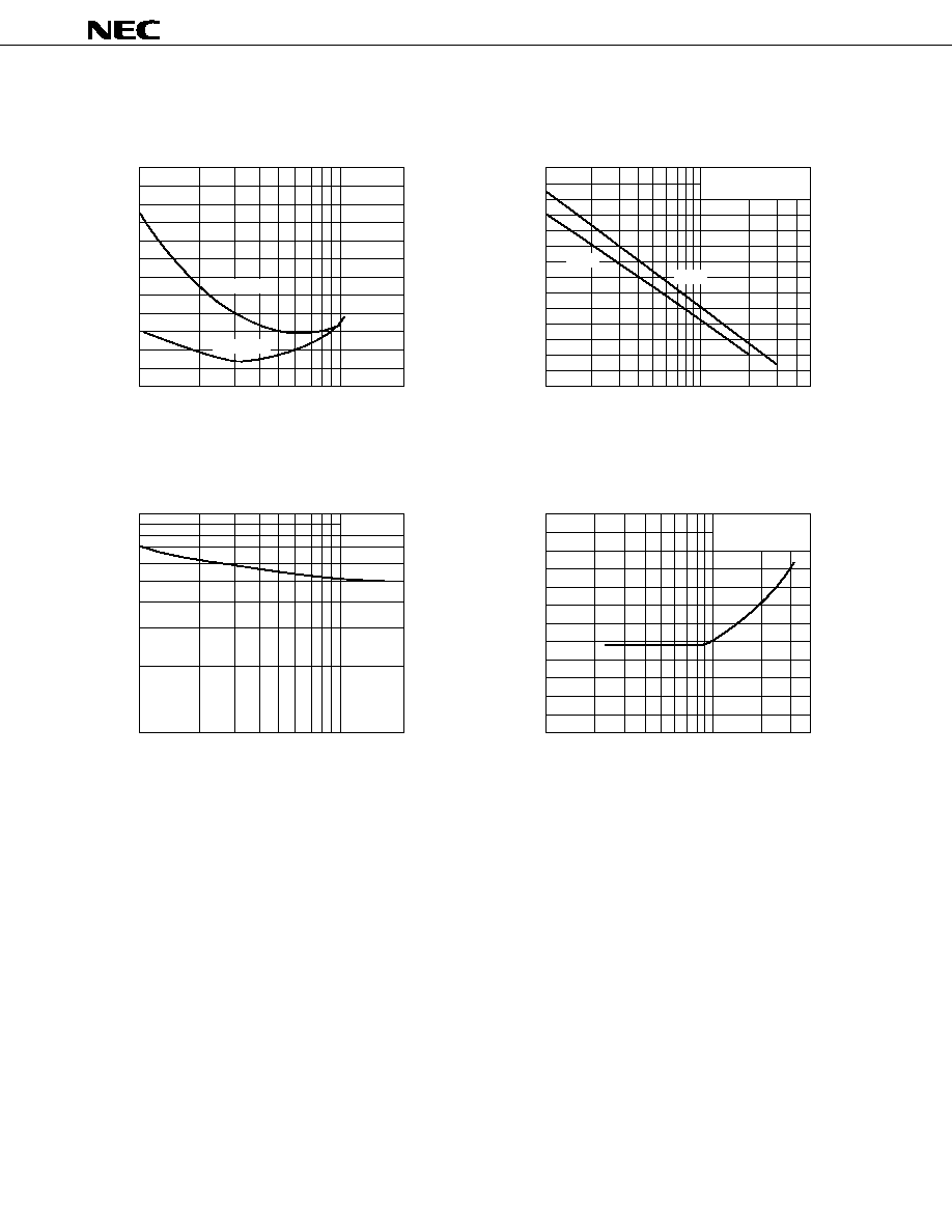
2SC5195
4
1
Collector Current I
C
(mA)
NOISE FIGURE vs.
COLLECTOR CURRENT
V
CE
= 1 V
Noise Figure NF (dB)
7
2
3
5
10
20
1
2
3
0.1
1
Collector to Base Voltage V
CB
(V)
FEED-BACK CAPACITANCE vs.
COLLECTOR TO BASE VOLTAGE
f = 1 MHz
Feed-back Capacitance C
re
(pF)
20
2
5
10
0.5
1.0
0
0.1
Frequency f (GHz)
MAXIMUM AVAILABLE GAIN / INSERTION
POWER GAIN vs. FREQUENCY
0.2
0.5
1
5
10
20
30
0.5
0.1
Frequency f (GHz)
Noise Figure NF (dB)
0.2
0.5
1
2
1.0
1.5
MAG
f = 2 GHz
f = 1 GHz
V
CE
= 1 V
I
C
= 5 mA
V
CE
= 1 V
I
C
= 5 mA
Maximum Available Power Gain MAG (dB)
Insertion Power Gain |S
21e
|
2
(dB)
|S
21e
|
2
NOISE FIGURE vs. FREQUENCY

2SC5195
5
S-PARAMETERS
V
CE
= 1 V, I
C
= 1 mA, Z
O
= 50
FREQUENCY
S11
S21
S12
S22
(MHz)
MAG
ANG
MAG
ANG
MAG
ANG
MAG
ANG
100.00
0.996
≠19.0
3.632
166.2
0.039
66.4
0.989
≠7.6
200.00
0.960
≠37.5
3.266
153.8
0.096
63.3
0.944
≠17.9
300.00
0.959
≠35.2
3.200
140.1
0.141
56.6
0.884
≠27.3
400.00
0.934
≠69.6
3.015
128.0
0.172
48.5
0.837
≠33.3
500.00
0.848
≠83.7
2.686
119.0
0.187
40.4
0.785
≠38.9
600.00
0.768
≠92.1
2.409
113.0
0.200
36.4
0.748
≠40.8
700.00
0.763
≠104.0
2.226
105.1
0.216
30.6
0.710
≠46.6
800.00
0.733
≠116.4
2.025
97.7
0.219
25.8
0.637
≠47.7
900.00
0.697
≠124.6
1.848
90.5
0.220
23.2
0.604
≠51.2
1000.00
0.678
≠137.7
1.703
86.1
0.218
21.1
0.361
≠52.7
1100.00
0.667
≠138.0
1.560
80.4
0.218
17.3
0.534
≠57.6
1200.00
0.673
≠147.0
1.510
75.9
0.212
13.7
0.514
≠62.6
1300.00
0.676
≠153.6
1.359
71.8
0.209
10.7
0.492
≠64.8
1400.00
0.689
≠160.2
1.270
70.0
0.207
9.7
0.478
≠63.7
1500.00
0.671
≠166.1
1.265
61.1
0.214
8.2
0.483
≠69.4
1600.00
0.644
≠170.8
1.240
55.7
0.213
8.9
0.471
≠73.4
1700.00
0.649
≠176.4
1.174
51.7
0.205
9.2
0.460
≠75.1
1800.00
0.605
176.0
1.183
49.6
0.197
11.7
0.450
≠79.2
1900.00
0.633
171.5
1.100
47.0
0.192
12.1
0.440
≠82.6
2000.00
0.640
165.5
1.034
45.8
0.184
13.3
0.442
≠86.1
V
CE
= 1 V, I
C
= 3 mA, Z
O
= 50
FREQUENCY
S11
S21
S12
S22
(MHz)
MAG
ANG
MAG
ANG
MAG
ANG
MAG
ANG
100.00
0.901
≠31.1
9.543
159.0
0.034
54.0
0.961
≠16.2
200.00
0.830
≠59.6
8.103
141.0
0.086
54.4
0.833
≠34.0
300.00
0.784
≠82.6
7.226
124.9
0.114
47.5
0.713
≠48.5
400.00
0.715
≠99.4
6.213
113.7
0.129
42.1
0.612
≠56.1
500.00
0.643
≠114.2
4.933
106.2
0.134
38.1
0.526
≠61.0
600.00
0.600
≠125.5
4.331
101.2
0.141
36.4
0.481
≠62.6
700.00
0.590
≠136.3
3.869
94.3
0.149
33.6
0.437
≠69.4
800.00
0.568
≠147.0
3.448
88.3
0.151
32.7
0.368
≠72.6
900.00
0.536
≠153.2
3.051
83.5
0.153
32.9
0.332
≠75.3
1000.00
0.535
≠160.4
2.791
80.1
0.157
33.4
0.304
≠77.1
1100.00
0.571
≠166.9
2.349
73.8
0.160
32.5
0.299
≠81.3
1200.00
0.536
≠173.3
2.398
72.1
0.161
31.8
0.280
≠88.2
1300.00
0.547
179.9
2.211
68.4
0.164
31.3
0.255
≠91.3
1400.00
0.536
178.2
2.098
65.8
0.169
31.6
0.241
≠95.0
1500.00
0.550
172.3
2.031
60.4
0.180
31.2
0.236
≠95.7
1600.00
0.528
169.3
1.920
56.3
0.189
32.1
0.231
≠100.8
1700.00
0.534
163.8
1.840
32.8
0.194
33.4
0.217
≠105.1
1800.00
0.517
158.2
1.740
51.4
0.198
35.5
0.214
110.3
1900.00
0.541
154.5
1.654
47.4
0.202
36.2
0.211
≠115.4
2000.00
0.550
150.2
1.558
48.0
0.203
36.7
0.216
≠118.6