DATA SHEET
Silicon Transistor
2SC5338
NPN EPITAXIAL SILICON TRANSISTOR
HIGH FREQUENCY LOW DISTORTION AMPLIFIER
1996
©
Document No. P10940EJ1V0DS00 (1st edition)
Date Published April 1996 P
Printed in Japan
PRELIMINARY DATA SHEET
DESCRIPTION
The 2SC5338 is designed for a low distortion and low noise RF amplifier with an operation on the low supply
voltage (V
CE
= 5 V). This low distortion characteristics is suitable for the CATV, tele-communication, and such.
FEATURES
PACKAGE DIMENSIONS
∑
High gain
(in millimeters)
|S
21
|
2
= 10 dB TYP., @V
CE
= 5 V, Ic = 50 mA, f = 1 GHz
∑
Low distortion and low voltage
IM
2
=
-
55 dB TYP., IM
3
=
-
76 dB TYP.
@V
CE
= 5 V, Ic = 50 mA, V
in
= 105 dB
µ
V/75
∑
New power mini-mold package version of a 4-pin type
gain-improved on the 2SC4703
ABSOLUTE MAXIMUM RATINGS (T
A
= 25 ∞C)
Parameter
Symbol
Rating
Unit
Collector to Base Voltage
V
CBO
25
V
Collector to Emitter Voltage
V
CEO
12
V
Emitter to Base Voltage
V
EBO
2.5
V
Collector Current
I
C
150
mA
Total Power Dissipation
P
T
Note1
1.8
W
Junction Temperature
T
j
150
∞
C
Storage Temperature
T
stg
≠65 to +150
∞
C
Note 1. 0.7 mm
◊
16 cm
2
double sided ceramic substrate (Copper plaiting)
1.6±0.2
2.45±0.1
3.95±0.25
1.5±0.1
0.25±0.02
0.42
±0.06
0.46
±0.06
3.0
1.5
0.42
±0.06
0.8 MIN.
PIN CONNECTIONS
E: Emitter
C: Collector
B: Base
C
E
B
E
4.5±0.1

2
2SC5338
ELECTRICAL CHARACTERISTICS (T
A
= 25
∞
∞
∞
∞
C)
Parameter
Symbol
Test Conditions
MIN.
TYP.
MAX.
Unit
Collector Cutoff Current
I
CBO
V
CB
= 20 V, I
E
= 0
1.5
µ
A
Emitter Cutoff Current
I
EBO
V
EB
= 2 V, I
C
= 0
1.5
µ
A
DC Current Gain
h
FE
V
CE
= 5 V, I
C
= 50 mA
Note2
50
250
Gain Bandwidth Product
f
T
V
CE
= 5 V, I
C
= 50 mA
6.0
GHz
Feed-back Capacitance
C
re
V
CB
= 5 V, I
E
= 0, f = 1 MHz
Note3
1.0
2.0
pF
Insertion Power Gain
|S
21e
|
2
V
CE
= 5 V, I
C
= 50 mA, f = 1 GHz
8.5
10
dB
Nose Figure
NF
V
CE
= 5 V, I
C
= 50 mA, f = 1 GHz
3.5
dB
IM
2
V
CE
= 5 V
-
55
dB
V
CE
= 10 V
-
63
IM
3
V
CE
= 5 V
-
76
dB
V
CE
= 10 V
-
83
Notes 2. Pulse measurement: PW
350
µ
S, Duty Cycle
2 %
3. Mesured by a 3-terminal bridge. Emitter and Case should be connected to the guard terminal.
h
FE
Classification
Rank
SH
SF
SE
Marking
SH
SF
SE
h
FE
50 to 100
80 to 160
125 to 250
3rd Order
Intermoduration
Distortion
2nd Order
Intermoduration
Distortion
I
C
= 50 mA
V
in
= 105 dB
µ
V/75
f = 190 MHz
-
90 MHz
I
C
= 50 mA
V
in
= 105 dB
µ
V/75
f = 2
◊
190 MHz
-
200 MHz

3
2SC5338
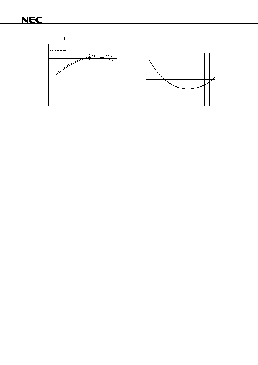
TYPICAL CHARACTERISTICS (T
A
= 25
∞
∞
∞
∞
C)
2
0
0.2
0.1
0.1
10
1
0.3
10
≠50
10
≠40
4
6
8
10
12
14
20
40
60
80
100
120
0.4
0.6
0.8
1.0
1.2
1
10
100
1000
3
5
10
20
30
0.5
1.0
2.0
3.0
5.0
20
50
100
200
≠60
≠70
≠80
≠90
20
50
100
200
≠50
≠60
≠70
1
10
100
1000
50
100
500
I
C
- Collector Current - mA
V
CE
- Collector to Emitter Voltage - V
I
C
- V
BE
Characteristics
I
C
- Collector Current - mA
V
BE
- Bese to Emitter Voltage - V
h
FE
- I
C
Characteristics
h
FE
- DC Current Gain
I
C
- Collector Current - mA
C
ob
- V
CB
Characteristics
C
re
- Feed-back Capacitance - pF
V
CB
- Collector to Base Voltage - V
IM
2
- I
C
Characteristics
IM
2
- 2nd Order Intermoduration Distortion - dB
I
C -
Collector Current - mA
IM
3
- I
C
Characteristics
IM
3
- 3rd Order Intermoduration Distortion - dB
I
C -
Collector Current - mA
I
B
= 0.7 mA
0.6
0.5
0.4
0.3
0.2
0.1
V
CE
= 10 V
5 V
f = 1.0 MH
Z
V
CE
= 10 V
5 V
V
O
= 105 dB V/75
f = 2
◊
190MHz ≠ 200 MH
Z
µ
V
CE
= 10 V
5 V
V
O
= 105 dB V/75
f = 190 MH
Z
≠ 90 MH
Z
µ
I
C
- V
CE
Characteristics
5 V
V
CE
= 10 V