 | –≠–ª–µ–∫—Ç—Ä–æ–Ω–Ω—ã–π –∫–æ–º–ø–æ–Ω–µ–Ω—Ç: 2SC5432 | –°–∫–∞—á–∞—Ç—å:  PDF PDF  ZIP ZIP |

©
1998
PRELIMINARY DATA SHEET
FEATURE
∑
Ultra super mini-mold thin flat package
(1.4 mm
◊
0.8 mm
◊
0.59 mm: TYP.)
∑
Contains same chip as 2SC5006
ABSOLUTE MAXIMUM RATINGS (T
A
= 25
∞
C)
PARAMETER
SYMBOL
RATING
UNIT
Collector to Base Voltage
V
CBO
20
V
Collector to Emitter Voltage
V
CEO
12
V
Emitter to Base Voltage
V
EBO
3
V
Collector Current
I
C
100
mA
Total Power Dissipation
P
T
125
mW
Junction Temperature
T
j
150
∞
C
Storage Temperature
T
stg
≠65 to +150
∞
C
SILICON TRANSISTOR
2SC5432
NPN EPITAXIAL SILICON TRANSISTOR
FOR HIGH-FREQUENCY LOW-NOISE AMPLIFICATION
Document No. P13076EJ1V0DS00 (1st edition)
Date Published February 1998 N CP(K)
Printed in Japan
ELECTRICAL CHARACTERISTICS (T
A
= 25
∞
C)
PARAMETER
SYMBOL
TEST CONDITIONS
MIN.
TYP.
MAX.
UNIT
Collector Cut-off Current
I
CBO
V
CB
= 10 V, I
E
= 0
1000
nA
Emitter Cut-off Current
I
EBO
V
EB
= 1 V, I
C
= 0
1000
nA
DC Current Gain
h
FE
V
CE
= 3 V, I
C
= 7 mA
Note 1
80
145
Gain Bandwidth Product
f
T
V
CE
= 3 V, I
C
= 7 mA, f = 1 GHz
3.0
4.5
GHz
Reverse Transfer Capacitance
C
re
V
CB
= 3 V, I
E
= 0, f = 1 MHz
Note 2
0.7
1.5
pF
Insertion Power Gain
|S
21e
|
2
V
CE
= 3 V, I
C
= 7 mA, f = 1 GHz
7.0
10.0
dB
Noise Figure
NF
V
CE
= 3 V, I
C
= 7 mA, f = 1 GHz
1.4
2.5
dB
Notes 1. Pulse measurement P
W
350
µ
s, duty cycle
2 %
2. Collector to base capacitance measured by capacitance meter (automatic balance bridge method) when
emitter pin is connected to the guard pin.
Because this product uses high-frequency process, avoid excessive input of static electricity, etc.
PACKAGE DIMENSIONS (in mm)
1.4 ± 0.05
0.8 ± 0.1
1.4 ± 0.1
0.59 ± 0.05
(0.9)
0.45
0.45
+0.1
≠0
0.3
+0.1
≠0.05
0.15
+0.1
≠0
0.2
1
3
2
T C
PIN CONNECTIONS
1: Emitter
2: Base
3: Collector
The information in this document is subject to change without notice.

2SC5432
2
Preliminary Data Sheet
h
FE
CLASSIFICATION
RANK
EB
FB
Marking
TC
TD
h
FE
80 to 110
100 to 145
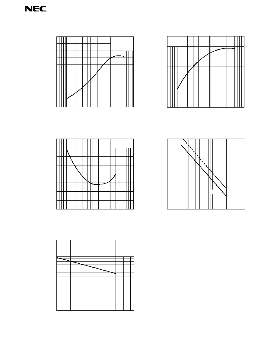
TYPICAL CHARACTERISTICS (T
A
= 25
∞
C)
COLLECTOR CURRENT vs. DC BASE VOLTAGE
I
C
- Collector Current - mA
20
0
10
1.0
0.5
V
BE
- DC Base Voltage - V
TOTAL POWER DISSIPATION
vs. AMBIENT TEMPERATURE
P
T
- Total Power Dissipation - mW
150
0
50
T
A
- Ambient Temperature - ∞C
150
100
50
100
DC CURRENT GAIN vs. COLLECTOR CURRENT
DC Current Gain - h
FE
I
C
- Collector Current - mA
COLLECTOR CURRENT vs.
COLLECTOR TO EMITTER VOLTAGE
I
C
- Collector Current - mA
25
V
CE
- Collector to Emitter Voltage - V
20
15
10
5
Free Air
V
CE
= 3 V
200
0.5
10
50
5
25
0
5
10
20
15
10
5
I
B
= 160 A
µ
140 A
120 A
100 A
80 A
60 A
40 A
20 A
20
10
2
1
100
20
50
V
CE
= 3 V
µ
µ
µ
µ
µ
µ
µ
2SC5432
3
Preliminary Data Sheet
MAXIMUM AVAILABLE GAIN/INSERTION
POWER GAIN vs. FREQUENCY
MAG - Maximum Available Gain - dB
|S
21e
|
2
- Insertion Power Gain - dB
25
0
5.0
0.5
f - Frequency - GHz
NOISE FIGURE vs. COLLECTOR CURRENT
NF - Noise Figure - dB
4
3
2
1
0
I
C
- Collector Current - mA
100
50
2
REVERSE TRANSFER CAPACITANCE
vs. COLLECTOR TO BASE VOLTAGE
C
re
- Reverse Transfer Capacitance - pF
2.0
1
2
V
CB
- Collector to Base Voltage - V
50
1.0
0.5
0.2
0.1
V
CE
= 3 V
I
C
= 7 mA
V
CE
= 3 V
f = 1 GH
Z
20
10
5
1
0.5
20
15
10
5
0.1
0.2
1.0
2.0
MAG
|S
21e
|
2
5
10
20
f = 1 MH
Z
INSERTION POWER GAIN
vs. COLLECTOR CURRENT
|S
21e
|
2
- Insertion Power Gain - dB
14
0.5
0
50
5
I
C
- Collector Current - mA
GAIN BANDWIDTH PRODUCT
vs. COLLECTOR CURRENT
f
T
- Gain Bandwidth Product - GHz
10
0
0.5
I
C
- Collector Current - mA
100
8
6
4
2
20
10
2
1
6
2
4
V
CE
= 3 V
f = 1 GH
Z
50
20
10
5
1
2
100
8
10
12
V
CE
= 3 V
f = 1 GH
Z

2SC5432
4
Preliminary Data Sheet
2SC5432 S PARAMETER
V
CE
= 3.0 V, I
C
= 10.0 mA, Z
0
= 50
FREQUENCY
S
11
S
21
S
12
S
22
MHz
MAG
ANG
MAG
ANG
MAG
ANG
MAG
ANG
200.00
0.575
≠108.7
14.215
118.3
0.048
48.3
0.524
≠55.9
400.00
0.548
≠145.7
8.064
98.2
0.062
45.8
0.295
≠73.7
600.00
0.540
≠161.8
5.617
87.4
0.075
49.0
0.213
≠84.1
800.00
0.539
≠173.0
4.354
81.5
0.087
53.0
0.173
≠90.5
1000.00
0.554
179.0
3.577
76.4
0.101
55.6
0.148
≠97.4
1200.00
0.574
174.1
3.038
70.8
0.117
57.3
0.132
≠105.9
1400.00
0.574
170.8
2.610
65.9
0.133
58.8
0.128
≠115.7
1600.00
0.565
165.8
2.306
62.4
0.148
60.3
0.128
≠124.7
1800.00
0.573
159.7
2.021
58.6
0.160
61.6
0.131
≠134.0
2000.00
0.598
155.4
1.802
54.8
0.172
60.7
0.137
≠144.8
2200.00
0.615
152.6
1.643
49.7
0.186
59.3
0.154
≠154.6
2400.00
0.628
150.0
1.553
45.8
0.204
58.4
0.176
≠160.5
2600.00
0.639
147.3
1.460
43.9
0.223
58.3
0.195
≠164.7
2800.00
0.655
144.8
1.331
41.4
0.236
58.7
0.214
≠168.6
3000.00
0.671
143.5
1.237
36.9
0.243
58.1
0.233
≠172.8
V
CE
= 3.0 V, I
C
= 7.0 mA, Z
0
= 50
FREQUENCY
S
11
S
21
S
12
S
22
MHz
MAG
ANG
MAG
ANG
MAG
ANG
MAG
ANG
200.00
0.630
≠95.3
12.557
123.1
0.055
47.9
0.609
≠47.7
400.00
0.576
≠136.3
7.443
101.8
0.071
41.3
0.359
≠64.2
600.00
0.561
≠155
5.246
89.3
0.082
42.8
0.264
≠72.8
800.00
0.554
≠167.6
4.082
82.7
0.091
46.0
0.218
≠77.8
1000.00
0.565
≠176.8
3.362
77.2
0.103
49.4
0.187
≠81.9
1200.00
0.586
177.4
2.865
71.2
0.115
51.8
0.166
≠87.6
1400.00
0.588
173.6
2.459
66.0
0.130
54.6
0.154
≠95.8
1600.00
0.577
168.2
2.176
62.2
0.142
56.9
0.150
≠104.6
1800.00
0.583
161.8
1.908
58.2
0.152
58.9
0.149
≠113.3
2000.00
0.607
157.1
1.700
54.2
0.163
58.5
0.150
≠123.7
2200.00
0.625
154.1
1.551
48.8
0.178
57.8
0.161
≠134.8
2400.00
0.639
151.3
1.468
44.7
0.194
57.4
0.181
≠143.4
2600.00
0.649
148.5
1.382
42.7
0.214
57.8
0.199
≠148.6
2800.00
0.665
145.8
1.256
40.1
0.227
58.5
0.219
≠153.9
3000.00
0.681
144.3
1.171
35.5
0.235
58.6
0.236
≠159.5
V
CE
= 3.0 V, I
C
= 5.0 mA, Z
0
= 50
FREQUENCY
S
11
S
21
S
12
S
22
MHz
MAG
ANG
MAG
ANG
MAG
ANG
MAG
ANG
200.00
0.693
≠81.4
10.462
129.2
0.063
50.6
0.699
≠39.3
400.00
0.610
≠125.1
6.572
105.9
0.083
39.0
0.442
≠54.7
600.00
0.588
≠146.4
4.723
92.0
0.093
37.7
0.334
≠62.8
800.00
0.575
≠160.7
3.713
84.4
0.098
38.5
0.284
≠67.1
1000.00
0.582
≠171.3
3.072
78.2
0.106
41.1
0.250
≠69.7
1200.00
0.600
≠178.3
2.566
71.8
0.116
43.9
0.226
≠73.2
1400.00
0.603
177.2
2.253
65.9
0.127
47.9
0.209
≠79.7
1600.00
0.590
171.4
1.997
61.8
0.135
51.6
0.199
≠86.9
1800.00
0.594
164.4
1.754
57.5
0.144
54.6
0.195
≠94.5
2000.00
0.619
159.2
1.563
53.1
0.153
55.4
0.192
≠103.2
2200.00
0.638
155.9
1.430
47.6
0.167
55.7
0.194
≠114.4
2400.00
0.651
152.8
1.352
43.4
0.182
56.3
0.211
≠124.6
2600.00
0.660
149.8
1.268
41.3
0.201
57.3
0.231
≠131.6
2800.00
0.677
147.0
1.149
38.5
0.214
58.8
0.249
≠137.8
3000.00
0.694
145.3
1.071
33.6
0.222
59.1
0.264
≠144.5

2SC5432
5
Preliminary Data Sheet
2SC5432 S PARAMETER
V
CE
= 3.0 V, I
C
= 3.0 mA, Z
0
= 50
FREQUENCY
S
11
S
21
S
12
S
22
MHz
MAG
ANG
MAG
ANG
MAG
ANG
MAG
ANG
200.00
0.782
≠65.7
7.726
136.8
0.073
54.2
0.804
≠29.6
400.00
0.669
≠109.9
5.283
111.9
0.101
38.4
0.563
≠43.8
600.00
0.639
≠134.2
3.921
95.9
0.111
32.3
0.445
≠52.1
800.00
0.616
≠150.6
3.139
87.0
0.113
30.0
0.392
≠56.7
1000.00
0.614
≠163.0
2.608
79.9
0.118
30.2
0.358
≠59.1
1200.00
0.629
≠171.7
2.194
72.4
0.122
32.5
0.331
≠61.7
1400.00
0.633
≠177.4
1.930
65.7
0.126
37.3
0.309
≠66.8
1600.00
0.617
176.2
1.716
61.1
0.128
42.2
0.296
≠73.3
1800.00
0.618
168.4
1.514
56.2
0.132
46.7
0.289
≠79.9
2000.00
0.642
162.5
1.349
51.7
0.137
49.0
0.285
≠87.4
2200.00
0.663
158.6
1.234
45.8
0.148
51.7
0.280
≠97.0
2400.00
0.676
155.2
1.167
41.4
0.162
54.2
0.292
≠107.5
2600.00
0.684
151.9
1.091
39.2
0.180
56.7
0.314
≠115.4
2800.00
0.698
148.7
0.985
36.2
0.195
59.3
0.330
≠122.1
3000.00
0.716
146.7
0.920
31.1
0.205
60.7
0.341
≠129.2
V
CE
= 3.0 V, I
C
= 1.0 mA, Z
0
= 50
FREQUENCY
S
11
S
21
S
12
S
22
MHz
MAG
ANG
MAG
ANG
MAG
ANG
MAG
ANG
200.00
0.914
≠43.7
3.280
148.3
0.086
62.7
0.936
≠15.4
400.00
0.795
≠82.1
2.575
123.7
0.139
43.0
0.792
≠26.4
600.00
0.769
≠109.7
2.086
104.4
0.161
30.5
0.689
≠35.5
800.00
0.731
≠128.9
1.783
91.7
0.164
21.2
0.648
≠42.3
1000.00
0.711
≠144.3
1.498
81.7
0.166
14.9
0.630
≠46.3
1200.00
0.715
≠156.5
1.286
72.2
0.162
12.3
0.603
≠49.8
1400.00
0.721
≠164.7
1.146
63.6
0.148
13.5
0.578
≠54.9
1600.00
0.700
≠172.6
1.029
57.8
0.134
15.4
0.559
≠61.5
1800.00
0.690
177.9
0.913
52.0
0.117
19.5
0.557
≠68.5
2000.00
0.711
170.1
0.817
46.8
0.107
25.1
0.552
≠75.6
2200.00
0.735
164.8
0.741
40.6
0.106
35.2
0.538
≠84.3
2400.00
0.746
160.3
0.702
36.4
0.110
46.3
0.547
≠94.8
2600.00
0.751
156.2
0.654
34.8
0.127
55.4
0.575
≠103.4
2800.00
0.763
152.2
0.587
32.3
0.146
63.2
0.589
≠110.3
3000.00
0.777
149.2
0.552
28.5
0.164
67.4
0.588
≠118.0
V
CE
= 1.0 V, I
C
= 5.0 mA, Z
0
= 50
FREQUENCY
S
11
S
21
S
12
S
22
MHz
MAG
ANG
MAG
ANG
MAG
ANG
MAG
ANG
200.00
0.678
≠95.9
9.388
123.0
0.082
44.1
0.611
≠54.6
400.00
0.630
≠137.1
5.585
100.5
0.100
34.1
0.363
≠78.9
600.00
0.615
≠155.7
3.937
87.4
0.109
33.2
0.274
≠93.7
800.00
0.609
≠168.4
3.084
80.3
0.115
34.5
0.228
≠103.2
1000.00
0.620
≠177.6
2.528
74.3
0.124
36.8
0.203
≠112.2
1200.00
0.641
176.7
2.121
67.5
0.135
39.3
0.192
≠121.5
1400.00
0.640
172.7
1.868
61.6
0.147
43.0
0.194
≠129.8
1600.00
0.626
167.2
1.656
57.6
0.157
46.4
0.199
≠136.6
1800.00
0.632
160.6
1.451
53.2
0.164
48.6
0.203
≠144.2
2000.00
0.657
155.8
1.300
48.9
0.173
49.0
0.214
≠152.4
2200.00
0.673
152.8
1.192
43.4
0.187
48.9
0.238
≠160.2
2400.00
0.685
149.8
1.128
39.5
0.203
49.5
0.265
≠164.8
2600.00
0.693
146.9
1.055
37.7
0.222
50.5
0.289
≠168.2
2800.00
0.708
144.3
0.960
35.0
0.232
51.6
0.311
≠172.0
3000.00
0.722
142.8
0.895
30.3
0.240
51.6
0.331
≠176.2

2SC5432
6
Preliminary Data Sheet
2SC5432 S PARAMETER
V
CE
= 1.0 V, I
C
= 3.0 mA, Z
0
= 50
FREQUENCY
S
11
S
21
S
12
S
22
MHz
MAG
ANG
MAG
ANG
MAG
ANG
MAG
ANG
200.00
0.754
≠77.4
7.160
130.9
0.097
48.5
0.729
≠40.9
400.00
0.668
≠121.7
4.630
106.0
0.126
32.9
0.469
≠61.1
600.00
0.644
≠143.9
3.356
90.7
0.134
27.4
0.359
≠73.2
800.00
0.630
≠158.8
2.664
82.0
0.136
25.4
0.306
≠80.5
1000.00
0.634
≠169.7
2.194
74.8
0.140
25.3
0.271
≠86.0
1200.00
0.653
≠177.1
1.850
67.1
0.145
27.6
0.250
≠92.7
1400.00
0.656
178.0
1.633
60.6
0.148
31.6
0.242
≠100.8
1600.00
0.640
172.0
1.448
56.1
0.151
36.1
0.241
≠108.6
1800.00
0.643
164.6
1.275
51.3
0.153
39.6
0.245
≠116.1
2000.00
0.667
159.3
1.139
46.5
0.158
41.4
0.248
≠125.3
2200.00
0.686
155.7
1.048
40.8
0.169
43.4
0.265
≠135.7
2400.00
0.698
152.5
0.988
36.7
0.181
45.9
0.295
≠143.4
2600.00
0.706
149.3
0.923
34.8
0.199
48.4
0.322
≠148.5
2800.00
0.721
146.4
0.833
32.1
0.211
50.5
0.346
≠153.8
3000.00
0.737
144.5
0.779
27.2
0.220
51.6
0.365
≠159.7
V
CE
= 1.0 V, I
C
= 1.0 mA, Z
0
= 50
FREQUENCY
S
11
S
21
S
12
S
22
MHz
MAG
ANG
MAG
ANG
MAG
ANG
MAG
ANG
200.00
0.893
≠49.6
3.192
143.8
0.119
59.2
0.903
≠21.2
400.00
0.773
≠90.6
2.404
117.2
0.180
37.9
0.720
≠35.3
600.00
0.745
≠117.4
1.906
97.3
0.203
25.0
0.610
≠46.5
800.00
0.711
≠135.9
1.603
84.7
0.205
15.4
0.564
≠54.0
1000.00
0.698
≠150.3
1.331
74.2
0.206
9.1
0.537
≠58.9
1200.00
0.708
≠161.3
1.148
64.2
0.199
6.5
0.511
≠63.9
1400.00
0.716
≠168.6
1.025
55.8
0.183
6.9
0.492
≠71.0
1600.00
0.696
≠176.0
0.916
50.0
0.165
7.9
0.483
≠79.0
1800.00
0.690
175.0
0.809
44.2
0.145
10.1
0.486
≠86.7
2000.00
0.714
167.7
0.719
39.0
0.131
13.9
0.482
≠95.1
2200.00
0.738
162.9
0.657
33.0
0.125
22.2
0.482
≠106.0
2400.00
0.750
158.7
0.619
29.3
0.126
32.3
0.508
≠116.7
2600.00
0.758
154.7
0.572
28.1
0.137
42.3
0.541
≠124.7
2800.00
0.770
150.9
0.513
26.2
0.152
50.5
0.559
≠131.8
3000.00
0.785
148.0
0.483
23.0
0.167
55.1
0.566
≠139.6

2SC5432
7
Preliminary Data Sheet
[MEMO]

2SC5432
2
No part of this document may be copied or reproduced in any form or by any means without the prior written
consent of NEC Corporation. NEC Corporation assumes no responsibility for any errors which may appear in
this document.
NEC Corporation does not assume any liability for infringement of patents, copyrights or other intellectual property
rights of third parties by or arising from use of a device described herein or any other liability arising from use
of such device. No license, either express, implied or otherwise, is granted under any patents, copyrights or other
intellectual property rights of NEC Corporation or others.
While NEC Corporation has been making continuous effort to enhance the reliability of its semiconductor devices,
the possibility of defects cannot be eliminated entirely. To minimize risks of damage or injury to persons or
property arising from a defect in an NEC semiconductor device, customers must incorporate sufficient safety
measures in its design, such as redundancy, fire-containment, and anti-failure features.
NEC devices are classified into the following three quality grades:
"Standard", "Special", and "Specific". The Specific quality grade applies only to devices developed based on a
customer designated "quality assurance program" for a specific application. The recommended applications of
a device depend on its quality grade, as indicated below. Customers must check the quality grade of each device
before using it in a particular application.
Standard: Computers, office equipment, communications equipment, test and measurement equipment,
audio and visual equipment, home electronic appliances, machine tools, personal electronic
equipment and industrial robots
Special:
Transportation equipment (automobiles, trains, ships, etc.), traffic control systems, anti-disaster
systems, anti-crime systems, safety equipment and medical equipment (not specifically designed
for life support)
Specific:
Aircrafts, aerospace equipment, submersible repeaters, nuclear reactor control systems, life
support systems or medical equipment for life support, etc.
The quality grade of NEC devices is "Standard" unless otherwise specified in NEC's Data Sheets or Data Books.
If customers intend to use NEC devices for applications other than those specified for Standard quality grade,
they should contact an NEC sales representative in advance.
Anti-radioactive design is not implemented in this product.
M4 96.5