 | –≠–ª–µ–∫—Ç—Ä–æ–Ω–Ω—ã–π –∫–æ–º–ø–æ–Ω–µ–Ω—Ç: 2SC5433 | –°–∫–∞—á–∞—Ç—å:  PDF PDF  ZIP ZIP |
©
1998
PRELIMINARY DATA SHEET
FEATURE
∑
Ultra super mini-mold thin flat package
(1.4 mm
◊
0.8 mm
◊
0.59 mm: TYP.)
∑
Contains same chip as 2SC5007
ABSOLUTE MAXIMUM RATINGS (T
A
= 25
∞
C)
PARAMETER
SYMBOL
RATING
UNIT
Collector to Base Voltage
V
CBO
20
V
Collector to Emitter Voltage
V
CEO
10
V
Emitter to Base Voltage
V
EBO
1.5
V
Collector Current
I
C
65
mA
Total Power Dissipation
P
T
125
mW
Junction Temperature
T
j
150
∞
C
Storage Temperature
T
stg
≠65 to +150
∞
C
SILICON TRANSISTOR
2SC5433
NPN EPITAXIAL SILICON TRANSISTOR
FOR HIGH-FREQUENCY LOW-NOISE AMPLIFICATION
Document No. P13077EJ1V0DS00 (1st edition)
Date Published February 1998 N CP(K)
Printed in Japan
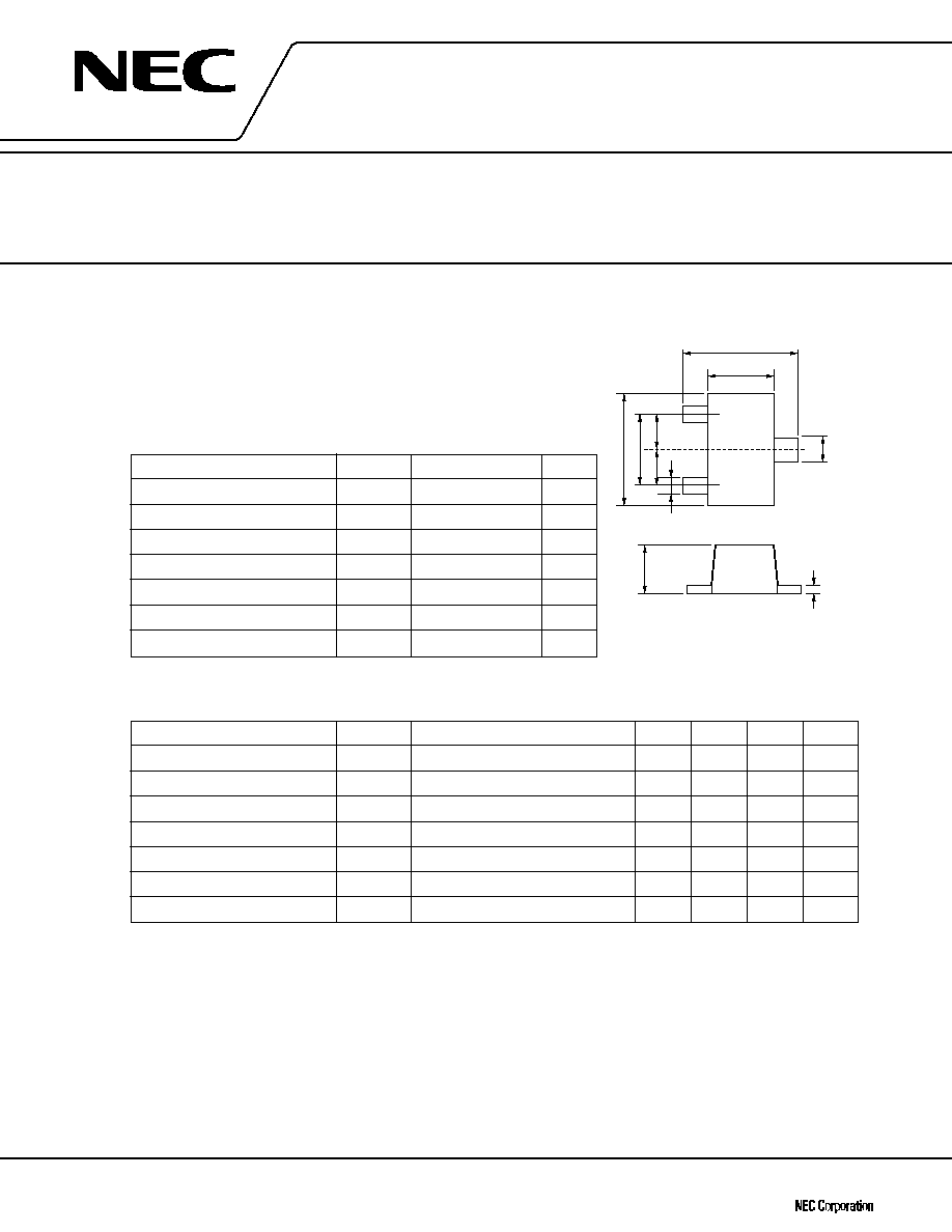
PACKAGE DIMENSIONS (in mm)
1.4 ± 0.05
0.8 ± 0.1
1.4 ± 0.1
0.59 ± 0.05
(0.9)
0.45
0.45
+0.1
≠0
0.3
+0.1
≠0.05
0.15
+0.1
≠0
0.2
1
3
2
T E
PIN CONNECTIONS
1: Emitter
2: Base
3: Collector
ELECTRICAL CHARACTERISTICS (T
A
= 25
∞
C)
PARAMETER
SYMBOL
TEST CONDITIONS
MIN.
TYP.
MAX.
UNIT
Collector Cut-off Current
I
CBO
V
CB
= 10 V, I
E
= 0
800
nA
Emitter Cut-off Current
I
EBO
V
EB
= 1 V, I
C
= 0
800
nA
DC Current Gain
h
FE
V
CE
= 3 V, I
C
= 7 mA
Note 1
80
145
Gain Bandwidth Product
f
T
V
CE
= 3 V, I
C
= 7 mA, f = 1 GHz
4.5
7.0
GHz
Reverse Transfer Capacitance
Cre
V
CB
= 3 V, I
E
= 0, f = 1 MHz
Note 2
0.9
pF
Insertion Power Gain
|S
21e
|
2
V
CE
= 3 V, I
C
= 7 mA, f = 1 GHz
10.0
12.0
dB
Noise Figure
NF
V
CE
= 3 V, I
C
= 7 mA, f = 1 GHz
1.4
2.7
dB
Notes 1. Pulse measurement P
W
350
µ
s, duty cycle
2 %
2. Collector to base capacitance measured by capacitance meter (automatic balance bridge method) when
emitter pin is connected to the guard pin.
Because this product uses high-frequency process, avoid excessive input of static electricity, etc.
The information in this document is subject to change without notice.
2SC5433
2
Preliminary Data Sheet
h
FE
CLASSIFICATION
RANK
EB
FB
Marking
TE
TF
h
FE
80 to 110
100 to 145
TYPICAL CHARACTERISTICS (T
A
= 25
∞
C)
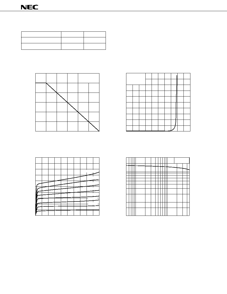
COLLECTOR CURRENT vs. DC BASE VOLTAGE
I
C
- Collector Current - mA
20
0
10
1.0
0.5
V
BE
- DC Base Voltage - V
TOTAL POWER DISSIPATION
vs. AMBIENT TEMPERATURE
P
T
- Total Power Dissipation - mW
150
0
50
T
A
- Ambient Temperature - ∞C
150
100
50
100
DC CURRENT GAIN vs. COLLECTOR CURRENT
DC Current Gain - h
FE
200
0.5
10
50
5
I
C
- Collector Current - mA
COLLECTOR CURRENT
vs. COLLECTOR TO EMITTER VOLTAGE
I
C
- Collector Current - mA
25
0
5
V
CE
- Collector to Emitter Voltage - V
10
20
15
10
5
Free Air
V
CE
= 3 V
I
B
= 160 A
140 A
120 A
100 A
80 A
60 A
40 A
20 A
µ
µ
µ
µ
µ
µ
µ
µ
20
10
2
1
100
20
50
V
CE
= 3 V
2SC5433
3
Preliminary Data Sheet
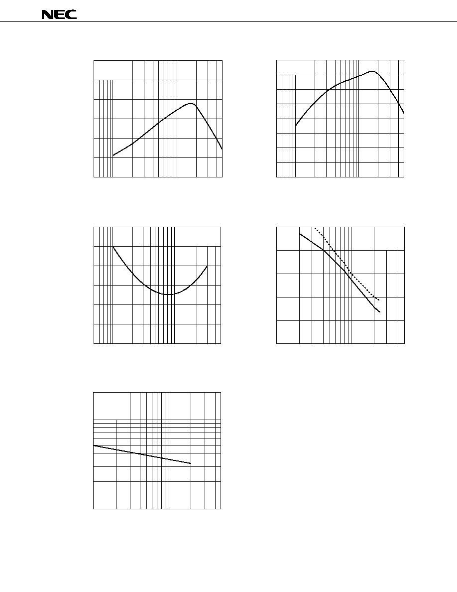
MAXIMUM AVAILABLE GAIN/INSERTION
POWER GAIN vs. FREQUENCY
MAG - Maximum Available Gain - dB
|S
21e
|
2
- Insertion Power Gain - dB
25
0
5.0
0.5
f - Frequency - GHz
NOISE FIGURE vs. COLLECTOR CURRENT
NF - Noise Figure - dB
3
0
1
I
C
- Collector Current - mA
50
2
2
REVERSE TRANSFER CAPACITANCE
vs. COLLECTOR TO BASE VOLTAGE
C
re
- Reverse Transfer Capacitance - pF
2.0
1
2
V
CB
- Collector to Base Voltage - V
50
1.0
0.5
0.2
0.1
V
CE
= 3 V
I
C
= 7 mA
20
10
5
1
0.5
20
15
10
5
0.1
0.2
1.0
2.0
MAG
|S
21e
|
2
5
10
20
f = 1 MH
Z
V
CE
= 3 V
f = GH
Z
INSERTION POWER GAIN
vs. COLLECTOR CURRENT
|S
21e
|
2
- Insertion Power Gain - dB
16
0.5
0
50
5
I
C
- Collector Current - mA
GAIN BANDWIDTH PRODUCT
vs. COLLECTOR CURRENT
f
T
- Gain Bandwidth Product - GHz
12
0
0.5
I
C
- Collector Current - mA
8
6
4
2
20
10
2
1
6
2
4
V
CE
= 3 V
f = 1 GH
Z
50
20
10
5
1
2
8
10
12
V
CE
= 3 V
f = 1 GH
Z
10
14

2SC5433
4
Preliminary Data Sheet
2SC5433 S PARAMETER
V
CE
= 3 V, I
C
= 10 mA, Z
0
= 50
FREQUENCY
S
11
S
21
S
12
S
22
MHz
MAG
ANG
MAG
ANG
MAG
ANG
MAG
ANG
200.00
0.593
≠73.5
17.349
130.6
0.036
58.5
0.701
≠33.6
400.00
0.470
≠115.9
10.897
108.5
0.051
53.7
0.454
≠43.4
600.00
0.435
≠138.3
7.822
95.9
0.063
55.3
0.348
≠47.0
800.00
0.418
≠153.3
6.134
89.3
0.075
57.9
0.300
≠48.0
1000.00
0.418
≠165.0
5.060
84.4
0.087
59.6
0.270
≠46.9
1200.00
0.431
≠172.7
4.321
79.2
0.100
61.1
0.243
≠45.7
1400.00
0.438
≠177.4
3.713
73.9
0.115
62.5
0.219
≠46.7
1600.00
0.432
176.8
3.234
70.3
0.129
63.8
0.196
≠49.6
1800.00
0.438
170.0
2.853
66.8
0.139
65.3
0.179
≠53.7
2000.00
0.461
164.5
2.564
63.4
0.150
64.6
0.164
≠58.5
2200.00
0.483
161.1
2.350
59.0
0.162
63.6
0.148
≠64.3
2400.00
0.499
158.4
2.213
55.1
0.178
62.5
0.134
≠73.7
2600.00
0.512
155.5
2.095
52.9
0.195
62.6
0.130
≠83.7
2800.00
0.529
152.8
1.922
50.8
0.207
63.5
0.127
≠92.6
3000.00
0.547
151.0
1.785
46.8
0.213
63.1
0.125
≠101.2
V
CE
= 3 V, I
C
= 7 mA, Z
0
= 50
FREQUENCY
S
11
S
21
S
12
S
22
MHz
MAG
ANG
MAG
ANG
MAG
ANG
MAG
ANG
200.00
0.673
≠61.7
14.941
136.5
0.040
61.6
0.773
≠29.2
400.00
0.523
≠103.4
10.008
113.4
0.058
51.9
0.527
≠41.0
600.00
0.474
≠127.5
7.335
99.6
0.070
51.2
0.406
≠46.4
800.00
0.444
≠144.1
5.814
91.9
0.080
52.6
0.349
≠48.3
1000.00
0.435
≠157.2
4.839
86.4
0.091
54.3
0.313
≠47.9
1200.00
0.444
≠166.4
4.135
80.8
0.102
56.2
0.281
≠47.0
1400.00
0.450
≠172.3
3.562
75.0
0.116
58.0
0.254
≠47.9
1600.00
0.442
≠178.6
3.109
71.0
0.128
60.2
0.228
≠50.6
1800.00
0.445
173.9
2.741
67.5
0.137
62.2
0.211
≠54.4
2000.00
0.466
167.7
2.474
63.9
0.146
61.8
0.195
≠58.5
2200.00
0.489
163.8
2.266
59.2
0.159
61.1
0.178
≠63.8
2400.00
0.505
160.7
2.136
55.1
0.173
60.3
0.164
≠72.0
2600.00
0.518
157.7
2.021
53.0
0.190
61.0
0.159
≠80.7
2800.00
0.534
154.6
1.855
50.6
0.201
62.2
0.157
≠88.3
3000.00
0.551
152.6
1.722
46.5
0.207
61.9
0.153
≠95.5
V
CE
= 3 V, I
C
= 5 mA, Z
0
= 50
FREQUENCY
S
11
S
21
S
12
S
22
MHz
MAG
ANG
MAG
ANG
MAG
ANG
MAG
ANG
200.00
0.759
≠50.6
12.082
142.5
0.045
62.8
0.844
≠24.2
400.00
0.593
≠89.5
8.740
119.7
0.067
51.4
0.615
≠36.8
600.00
0.533
≠115.2
6.641
104.4
0.080
47.9
0.483
≠44.2
800.00
0.487
≠132.9
5.367
95.5
0.088
47.5
0.418
≠47.3
1000.00
0.467
≠147.3
4.496
89.2
0.097
48.2
0.376
≠47.5
1200.00
0.468
≠158.3
3.871
83.0
0.107
49.6
0.338
≠46.9
1400.00
0.473
≠165.5
3.337
76.7
0.118
52.2
0.306
≠48.2
1600.00
0.462
≠172.6
2.925
72.2
0.127
55.0
0.277
≠50.6
1800.00
0.460
179.1
2.585
68.2
0.135
57.1
0.258
≠54.1
2000.00
0.479
171.9
2.349
64.7
0.142
57.2
0.241
≠57.8
2200.00
0.502
167.4
2.139
59.5
0.154
57.4
0.224
≠62.4
2400.00
0.518
163.9
2.017
55.1
0.166
57.3
0.209
≠69.5
2600.00
0.529
160.4
1.908
52.8
0.182
58.6
0.204
≠76.9
2800.00
0.544
157.1
1.752
50.1
0.192
60.3
0.202
≠83.4
3000.00
0.562
154.8
1.631
45.8
0.198
60.5
0.195
≠89.3

2SC5433
5
Preliminary Data Sheet
2SC5433 S PARAMETER
V
CE
= 3 V, I
C
= 3 mA, Z
0
= 50
FREQUENCY
S
11
S
21
S
12
S
22
MHz
MAG
ANG
MAG
ANG
MAG
ANG
MAG
ANG
200.00
0.849
≠39.1
8.593
149.9
0.049
67.9
0.910
≠18.1
400.00
0.690
≠72.9
6.799
128.1
0.078
53.3
0.728
≠30.3
600.00
0.626
≠99.3
5.461
111.5
0.096
46.0
0.595
≠39.2
800.00
0.565
≠117.8
4.546
101.0
0.104
42.3
0.525
≠44.2
1000.00
0.528
≠133.4
3.893
93.5
0.111
40.7
0.478
≠45.5
1200.00
0.515
≠146.4
3.387
86.5
0.118
40.9
0.433
≠45.6
1400.00
0.515
≠155.4
2.949
79.2
0.126
43.1
0.394
≠47.1
1600.00
0.500
≠163.5
2.631
74.4
0.130
46.1
0.360
≠49.6
1800.00
0.490
≠172.8
2.342
69.8
0.134
48.8
0.339
≠53.2
2000.00
0.505
178.7
2.095
65.4
0.137
49.3
0.322
≠56.7
2200.00
0.528
173.1
1.910
59.7
0.146
50.5
0.302
≠60.7
2400.00
0.543
168.9
1.808
54.9
0.156
51.9
0.287
≠66.9
2600.00
0.553
164.9
1.713
52.3
0.169
53.8
0.283
≠73.6
2800.00
0.566
161.0
1.571
49.3
0.177
56.6
0.284
≠79.0
3000.00
0.583
158.0
1.464
44.8
0.182
57.8
0.276
≠84.0
V
CE
= 3 V, I
C
= 1 mA, Z
0
= 50
FREQUENCY
S
11
S
21
S
12
S
22
MHz
MAG
ANG
MAG
ANG
MAG
ANG
MAG
ANG
200.00
0.955
≠23.9
3.465
160.1
0.053
73.5
0.977
≠9.3
400.00
0.852
≠47.2
3.060
142.4
0.097
60.6
0.894
≠17.6
600.00
0.803
≠71.0
2.702
126.3
0.130
49.7
0.802
≠26.5
800.00
0.759
≠88.9
2.480
113.4
0.147
41.4
0.754
≠33.8
1000.00
0.710
≠104.8
2.263
103.8
0.159
34.0
0.723
≠37.4
1200.00
0.667
≠119.3
1.995
95.1
0.167
29.3
0.677
≠39.2
1400.00
0.653
≠131.7
1.791
85.4
0.169
27.8
0.630
≠41.7
1600.00
0.632
≠141.9
1.654
78.2
0.164
27.1
0.589
≠45.0
1800.00
0.602
≠152.6
1.508
72.1
0.154
26.6
0.565
≠49.1
2000.00
0.599
≠163.9
1.359
66.4
0.147
25.0
0.549
≠53.3
2200.00
0.621
≠172.4
1.256
59.2
0.143
26.8
0.529
≠57.3
2400.00
0.635
≠178.4
1.200
53.7
0.139
30.1
0.511
≠63.4
2600.00
0.639
176.3
1.137
50.5
0.138
34.9
0.513
≠70.0
2800.00
0.645
171.0
1.038
46.5
0.136
41.1
0.522
≠75.1
3000.00
0.659
166.4
0.976
41.4
0.135
46.7
0.512
≠79.8
V
CE
= 1 V, I
C
= 5 mA, Z
0
= 50
FREQUENCY
S
11
S
21
S
12
S
22
MHz
MAG
ANG
MAG
ANG
MAG
ANG
MAG
ANG
200.00
0.732
≠59.6
11.569
138.4
0.055
60.0
0.790
≠31.6
400.00
0.588
≠101.6
8.006
115.1
0.081
47.5
0.536
≠48.4
600.00
0.543
≠126.5
5.948
100.2
0.094
44.0
0.403
≠58.2
800.00
0.511
≠143.6
4.748
91.7
0.102
43.7
0.334
≠63.0
1000.00
0.501
≠156.8
3.960
85.6
0.112
44.2
0.283
≠64.7
1200.00
0.511
≠166.4
3.400
79.2
0.123
45.5
0.243
≠66.6
1400.00
0.516
≠172.5
2.936
73.0
0.135
47.9
0.213
≠70.5
1600.00
0.505
≠179.0
2.602
69.1
0.145
50.7
0.189
≠75.6
1800.00
0.506
173.1
2.296
65.0
0.153
52.4
0.170
≠81.5
2000.00
0.527
166.8
2.047
61.0
0.161
52.3
0.157
≠88.6
2200.00
0.548
162.8
1.865
55.7
0.173
52.1
0.144
≠99.3
2400.00
0.564
159.5
1.761
51.5
0.186
52.1
0.144
≠110.9
2600.00
0.574
156.2
1.661
49.1
0.202
53.0
0.150
≠119.7
2800.00
0.588
153.1
1.521
46.6
0.210
54.2
0.156
≠127.5
3000.00
0.605
151.0
1.415
42.1
0.217
54.2
0.163
≠134.9

2SC5433
6
Preliminary Data Sheet
2SC5433 S PARAMETER
V
CE
= 1 V, I
C
= 3 mA, Z
0
= 50
FREQUENCY
S
11
S
21
S
12
S
22
MHz
MAG
ANG
MAG
ANG
MAG
ANG
MAG
ANG
200.00
0.829
≠45.4
8.382
146.5
0.061
64.5
0.878
≠23.6
400.00
0.673
≠82.9
6.392
123.5
0.097
49.0
0.662
≠39.2
600.00
0.619
≠109.4
5.005
106.9
0.115
41.6
0.521
≠50.1
800.00
0.568
≠127.9
4.115
96.8
0.122
38.0
0.444
≠56.0
1000.00
0.542
≠143.0
3.493
89.2
0.130
36.2
0.387
≠58.3
1200.00
0.540
≠154.9
3.029
82.2
0.138
36.4
0.340
≠59.8
1400.00
0.543
≠162.7
2.607
75.3
0.146
38.7
0.301
≠63.0
1600.00
0.529
≠170.3
2.338
70.4
0.149
41.4
0.271
≠67.1
1800.00
0.522
≠179.2
2.072
65.8
0.153
43.4
0.251
≠71.8
2000.00
0.540
173.2
1.850
61.3
0.156
43.6
0.234
≠76.9
2200.00
0.563
168.2
1.692
55.5
0.165
44.5
0.215
≠84.6
2400.00
0.577
164.4
1.598
51.0
0.176
45.8
0.209
≠93.4
2600.00
0.586
160.6
1.511
48.4
0.188
47.7
0.213
≠101.4
2800.00
0.600
157.1
1.382
45.4
0.195
49.7
0.216
≠108.0
3000.00
0.616
154.4
1.288
40.7
0.199
50.6
0.217
≠114.8
V
CE
= 1 V, I
C
= 1 mA, Z
0
= 50
FREQUENCY
S
11
S
21
S
12
S
22
MHz
MAG
ANG
MAG
ANG
MAG
ANG
MAG
ANG
200.00
0.947
≠26.7
3.453
158.0
0.068
72.9
0.967
≠11.9
400.00
0.835
≠52.6
2.996
138.7
0.123
57.4
0.863
≠22.3
600.00
0.787
≠77.5
2.609
121.6
0.161
45.7
0.757
≠32.9
800.00
0.738
≠95.9
2.363
108.5
0.178
36.8
0.699
≠40.9
1000.00
0.692
≠112.1
2.118
98.6
0.192
29.0
0.654
≠44.9
1200.00
0.656
≠126.6
1.853
89.4
0.200
24.3
0.602
≠47.4
1400.00
0.648
≠138.2
1.663
79.7
0.201
22.9
0.554
≠50.7
1600.00
0.629
≠148.0
1.528
72.7
0.194
21.7
0.513
≠55.0
1800.00
0.603
≠158.4
1.385
66.6
0.182
20.6
0.490
≠59.6
2000.00
0.606
≠169.1
1.247
60.9
0.173
18.5
0.472
≠64.2
2200.00
0.629
≠176.8
1.156
53.8
0.169
19.6
0.448
≠69.6
2400.00
0.643
177.7
1.100
48.3
0.163
22.6
0.437
≠77.1
2600.00
0.649
172.8
1.039
45.1
0.159
26.0
0.445
≠84.3
2800.00
0.656
167.8
0.945
41.3
0.153
31.0
0.452
≠89.8
3000.00
0.672
163.6
0.886
35.9
0.151
35.5
0.444
≠95.4

2SC5433
7
Preliminary Data Sheet
[MEMO]

2SC5433
2
No part of this document may be copied or reproduced in any form or by any means without the prior written
consent of NEC Corporation. NEC Corporation assumes no responsibility for any errors which may appear in
this document.
NEC Corporation does not assume any liability for infringement of patents, copyrights or other intellectual property
rights of third parties by or arising from use of a device described herein or any other liability arising from use
of such device. No license, either express, implied or otherwise, is granted under any patents, copyrights or other
intellectual property rights of NEC Corporation or others.
While NEC Corporation has been making continuous effort to enhance the reliability of its semiconductor devices,
the possibility of defects cannot be eliminated entirely. To minimize risks of damage or injury to persons or
property arising from a defect in an NEC semiconductor device, customers must incorporate sufficient safety
measures in its design, such as redundancy, fire-containment, and anti-failure features.
NEC devices are classified into the following three quality grades:
"Standard", "Special", and "Specific". The Specific quality grade applies only to devices developed based on a
customer designated "quality assurance program" for a specific application. The recommended applications of
a device depend on its quality grade, as indicated below. Customers must check the quality grade of each device
before using it in a particular application.
Standard: Computers, office equipment, communications equipment, test and measurement equipment,
audio and visual equipment, home electronic appliances, machine tools, personal electronic
equipment and industrial robots
Special:
Transportation equipment (automobiles, trains, ships, etc.), traffic control systems, anti-disaster
systems, anti-crime systems, safety equipment and medical equipment (not specifically designed
for life support)
Specific:
Aircrafts, aerospace equipment, submersible repeaters, nuclear reactor control systems, life
support systems or medical equipment for life support, etc.
The quality grade of NEC devices is "Standard" unless otherwise specified in NEC's Data Sheets or Data Books.
If customers intend to use NEC devices for applications other than those specified for Standard quality grade,
they should contact an NEC sales representative in advance.
Anti-radioactive design is not implemented in this product.
M4 96.5