 | –≠–ª–µ–∫—Ç—Ä–æ–Ω–Ω—ã–π –∫–æ–º–ø–æ–Ω–µ–Ω—Ç: 2SC5434 | –°–∫–∞—á–∞—Ç—å:  PDF PDF  ZIP ZIP |
©
1998
PRELIMINARY DATA SHEET
FEATURE
∑
Ultra super mini-mold thin flat package
(1.4 mm
◊
1.8 mm
◊
0.59 mm: TYP.)
∑
Contains same chip as 2SC5008
ABSOLUTE MAXIMUM RATINGS (T
A
= 25
∞
C)
PARAMETER
SYMBOL
RATING
UNIT
Collector to Base Voltage
V
CBO
20
V
Collector to Emitter Voltage
V
CEO
10
V
Emitter to Base Voltage
V
EBO
1.5
V
Collector Current
I
C
35
mA
Total Power Dissipation
P
T
125
mW
Junction Temperature
T
j
150
∞
C
Storage Temperature
T
stg
≠65 to +150
∞
C
SILICON TRANSISTOR
2SC5434
NPN EPITAXIAL SILICON TRANSISTOR
FOR HIGH-FREQUENCY LOW-NOISE AMPLIFICATION
Document No. P13145EJ1V0DS00 (1st edition)
Date Published February 1998 N CP(K)
Printed in Japan
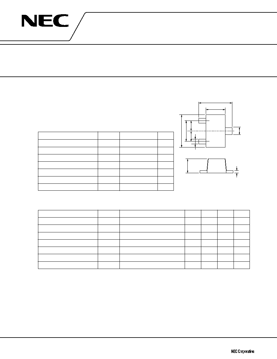
PACKAGE DIMENSIONS (in mm)
1.4 ± 0.05
0.8 ± 0.1
1.4 ± 0.1
0.59 ± 0.05
(0.9)
0.45
0.45
+0.1
≠0
0.3
+0.1
≠0.05
0.15
+0.1
≠0
0.2
1
3
2
T H
PIN CONNECTIONS
1: Emitter
2: Base
3: Collector
ELECTRICAL CHARACTERISTICS (T
A
= 25
∞
C)
PARAMETER
SYMBOL
TEST CONDITIONS
MIN.
TYP.
MAX.
UNIT
Collector Cut-off Current
I
CBO
V
CB
= 10 V, I
E
= 0
1000
nA
Emitter Cut-off Current
I
EBO
V
EB
= 1 V, I
C
= 0
1000
nA
DC Current Gain
h
FE
V
CE
= 3 V, I
C
= 5 mA
Note 1
80
145
Gain Bandwidth Product
f
T
V
CE
= 3 V, I
C
= 5 mA, f = 2 GHz
5.5
80
GHz
Reverse Transfer Capacitance
C
re
V
CB
= 3 V, I
E
= 0, f = 1 MHz
Note 2
0.3
0.7
pF
Insertion Power Gain
|S
21e
|
2
V
CE
= 3 V, I
C
= 5 mA, f = 2 GHz
5.5
7.5
dB
Noise Figure
NF
V
CE
= 3 V, I
C
= 5 mA, f = 2 GHz
1.9
3.2
dB
Notes 1. Pulse measurement P
W
350
µ
s, duty cycle
2 %
2. Collector to base capacitance measured by capacitance meter (automatic balance bridge method) when
emitter pin is connected to the guard pin.
Because this product uses high-frequency process, avoid excessive input of static electricity, etc.
The information in this document is subject to change without notice.

2SC5434
2
Preliminary Data Sheet
h
FE
CLASSIFICATION
RANK
EB
FB
Marking
TH
TJ
h
FE
80 to 110
100 to 145
TYPICAL CHARACTERISTICS (T
A
= 25
∞
C)
I
C
- Collector Current - mA
20
0
10
1.0
0.5
V
BE
- DC Base Voltage - V
TOTAL POWER DISSIPATION
vs. AMBIENT TEMPERATURE
DC CURRENT GAIN vs. COLLECTOR CURRENT
COLLECTOR CURRENT vs.
COLLECTOR TO EMITTER VOLTAGE
COLLECTOR CURRENT vs. DC BASE VOLTAGE
P
T
- Total Power Dissipation - mW
150
0
50
T
A
- Ambient Temperature - ∞C
150
100
50
100
DC Current Gain - h
FE
200
0.5
10
50
5
I
C
- Collector Current - mA
I
C
- Collector Current - mA
25
0
5
V
CE
- Collector to Emitter Voltage - V
10
20
15
10
5
Free Air
V
CE
= 3 V
I
B
= 160 A
µ
140 A
µ
120 A
µ
100 A
µ
80 A
µ
60 A
µ
40 A
µ
20 A
µ
20
10
2
1
100
20
50
V
CE
= 3 V

2SC5434
3
Preliminary Data Sheet
MAXIMUM AVAILABLE GAIN/INSERTION
POWER GAIN vs. FREQUENCY
35
0
10.0
1.0
f - Frequency - GHz
NOISE FIGURE vs. COLLECTOR CURRENT
NF - Noise Figure - dB
7.00
0.00
3.00
4.00
1.00
2.00
I
C
- Collector Current - mA
50
5.00
6.00
REVERSE TRANSFER CAPACITANCE
vs. COLLECTOR TO BASE VOLTAGE
C
re
- Reverse Transfer Capacitance - pF
1
V
CB
- Collector to Base Voltage - V
100
1.00
0.10
V
CE
= 3 V
I
C
= 5 mA
10
1
25
30
20
15
10
5
0.1
10
f = 1 MH
Z
V
CE
= 3 V
f = 2 GH
Z
INSERTION POWER GAIN
vs. COLLECTOR CURRENT
|S
21e
|
2
- Insertion Power Gain - dB
1
0
2
4
6
8
10
12
14
16
100
10
I
C
- Collector Current - mA
GAIN BANDWIDTH PRODUCT
vs. COLLECTOR CURRENT
f
T
- Gain Bandwidth Product - GHz
9
8
0
1
I
C
- Collector Current - mA
4
3
2
1
V
CE
= 3 V
f = 2 GH
Z
V
CE
= 3 V
f = 2 GH
Z
100
10
7
6
5
MAG
|S
21e
|
2
MAG - Maximum Available Gain - dB
|S
21e
|
2
- Insertion Power Gain - dB

2SC5434
4
Preliminary Data Sheet
2SC5434 S PARAMETER
V
CE
= 3 V, I
C
= 10 mA, Z
0
= 50
FREQUENCY
S
11
S
21
S
12
S
22
MHz
MAG
ANG
MAG
ANG
MAG
ANG
MAG
ANG
200.00
0.589
≠46.2
15.156
134.5
0.027
63.5
0.772
≠23.5
400.00
0.366
≠73.1
9.926
112.1
0.038
58.9
0.561
≠28.9
600.00
0.265
≠91.3
7.179
99.2
0.048
59.0
0.465
≠30.3
800.00
0.205
≠104.1
5.703
92.4
0.056
61.0
0.429
≠31.0
1000.00
0.165
≠117.4
4.740
87.6
0.066
62.6
0.415
≠30.3
1200.00
0.143
≠132.6
4.069
82.7
0.077
63.9
0.398
≠28.6
1400.00
0.135
≠145.6
3.508
77.5
0.088
64.8
0.377
≠28.4
1600.00
0.131
≠158.5
3.075
73.8
0.100
65.9
0.353
≠29.4
1800.00
0.133
≠171.6
2.729
70.5
0.110
68.1
0.335
≠31.9
2000.00
0.146
176.2
2.474
67.2
0.120
67.3
0.323
≠35.1
2200.00
0.166
168.7
2.285
62.9
0.130
66.7
0.312
≠37.1
2400.00
0.184
164.3
2.154
58.8
0.143
65.6
0.293
≠40.2
2600.00
0.200
159.7
2.057
56.3
0.158
65.6
0.278
≠44.5
2800.00
0.218
155.6
1.918
54.3
0.168
66.4
0.273
≠49.0
3000.00
0.236
152.9
1.785
50.7
0.175
65.8
0.265
≠52.6
V
CE
= 3 V, I
C
= 7 mA, Z
0
= 50
FREQUENCY
S
11
S
21
S
12
S
22
MHz
MAG
ANG
MAG
ANG
MAG
ANG
MAG
ANG
200.00
0.687
≠38.0
13.645
140.8
0.030
66.7
0.830
≠21.6
400.00
0.458
≠63.0
9.604
118.2
0.044
58.2
0.613
≠30.3
600.00
0.339
≠80.5
7.166
104.1
0.054
56.2
0.497
≠34.0
800.00
0.264
≠92.0
5.746
96.1
0.062
57.4
0.447
≠35.5
1000.00
0.210
≠102.5
4.830
90.8
0.072
58.2
0.422
≠34.6
1200.00
0.172
≠115.0
4.162
85.7
0.082
59.5
0.396
≠32.8
1400.00
0.153
≠127.5
3.604
80.1
0.093
60.3
0.370
≠32.5
1600.00
0.141
≠140.3
3.164
76.0
0.105
62.1
0.343
≠33.4
1800.00
0.134
≠154.2
2.816
72.5
0.114
64.1
0.324
≠35.5
2000.00
0.139
≠168.8
2.546
69.0
0.122
64.1
0.309
≠38.2
2200.00
0.155
≠179.6
2.355
64.7
0.133
63.2
0.296
≠40.0
2400.00
0.172
173.9
2.219
60.5
0.145
62.2
0.276
≠43.1
2600.00
0.187
168.0
2.120
57.9
0.159
62.4
0.261
≠47.1
2800.00
0.203
162.6
1.983
55.9
0.170
63.3
0.255
≠51.5
3000.00
0.221
159.0
1.843
52.3
0.176
62.9
0.247
≠54.9
V
CE
= 3 V, I
C
= 5 mA, Z
0
= 50
FREQUENCY
S
11
S
21
S
12
S
22
MHz
MAG
ANG
MAG
ANG
MAG
ANG
MAG
ANG
200.00
0.777
≠30.9
11.368
147.0
0.032
69.9
0.883
≠18.7
400.00
0.562
≠53.6
8.634
125.2
0.051
57.8
0.688
≠29.1
600.00
0.431
≠71.4
6.753
109.9
0.062
53.9
0.559
≠35.3
800.00
0.344
≠82.7
5.525
100.7
0.071
53.6
0.496
≠38.3
1000.00
0.273
≠91.9
4.677
94.6
0.080
53.4
0.460
≠38.2
1200.00
0.220
≠102.3
4.070
88.9
0.089
53.9
0.424
≠36.8
1400.00
0.189
≠113.6
3.534
82.8
0.099
54.9
0.391
≠36.7
1600.00
0.165
≠125.3
3.113
78.1
0.109
57.1
0.358
≠37.6
1800.00
0.149
≠138.6
2.768
74.2
0.118
58.9
0.336
≠39.7
2000.00
0.143
≠154.5
2.513
70.6
0.125
58.9
0.319
≠42.1
2200.00
0.153
≠168.3
2.326
65.9
0.135
58.2
0.303
≠43.9
2400.00
0.167
≠177.1
2.189
61.6
0.146
57.8
0.282
≠47.1
2600.00
0.180
175.5
2.092
58.8
0.160
58.0
0.266
≠51.3
2800.00
0.194
168.8
1.955
56.7
0.168
59.4
0.259
≠55.2
3000.00
0.210
163.5
1.819
53.1
0.174
59.0
0.252
≠58.5

2SC5434
5
Preliminary Data Sheet
2SC5434 S PARAMETER
V
CE
= 3 V, I
C
= 3 mA, Z
0
= 50
FREQUENCY
S
11
S
21
S
12
S
22
MHz
MAG
ANG
MAG
ANG
MAG
ANG
MAG
ANG
200.00
0.866
≠23.3
8.242
154.2
0.034
73.1
0.934
≠14.4
400.00
0.693
≠42.6
6.829
134.4
0.058
61.3
0.784
≠24.9
600.00
0.565
≠60.3
5.662
118.8
0.075
54.0
0.657
≠33.3
800.00
0.474
≠72.1
4.819
108.1
0.084
51.0
0.588
≠38.5
1000.00
0.390
≠80.9
4.196
101.0
0.092
48.6
0.543
≠39.9
1200.00
0.321
≠89.8
3.702
94.7
0.102
47.7
0.495
≠39.5
1400.00
0.274
≠99.4
3.260
87.8
0.111
48.6
0.453
≠40.0
1600.00
0.237
≠109.3
2.889
82.1
0.119
50.7
0.413
≠41.4
1800.00
0.209
≠119.5
2.590
77.8
0.124
52.1
0.386
≠43.8
2000.00
0.187
≠133.1
2.383
74.0
0.130
51.9
0.365
≠46.2
2200.00
0.183
≠147.1
2.189
68.7
0.138
51.5
0.344
≠48.2
2400.00
0.190
≠157.5
2.066
63.9
0.148
51.3
0.321
≠51.6
2600.00
0.197
≠166.2
1.982
60.8
0.161
52.3
0.306
≠55.8
2800.00
0.204
≠174.4
1.861
58.4
0.167
53.7
0.299
≠59.6
3000.00
0.215
178.1
1.735
54.5
0.171
53.6
0.289
≠62.5
V
CE
= 3 V, I
C
= 1 mA, Z
0
= 50
FREQUENCY
S
11
S
21
S
12
S
22
MHz
MAG
ANG
MAG
ANG
MAG
ANG
MAG
ANG
200.00
0.959
≠12.8
3.416
164.4
0.038
79.7
0.984
≠7.5
400.00
0.880
≠24.9
3.110
150.1
0.070
68.7
0.922
≠14.6
600.00
0.792
≠38.9
2.829
136.8
0.097
60.3
0.843
≠22.9
800.00
0.739
≠50.7
2.654
125.2
0.118
53.8
0.801
≠30.5
1000.00
0.669
≠59.5
2.539
116.6
0.132
47.5
0.774
≠34.6
1200.00
0.590
≠67.2
2.307
109.5
0.146
42.7
0.726
≠36.6
1400.00
0.520
≠75.5
2.081
100.9
0.159
40.4
0.670
≠39.0
1600.00
0.458
≠84.6
1.965
93.1
0.163
39.4
0.616
≠42.0
1800.00
0.412
≠92.6
1.839
87.1
0.164
38.3
0.579
≠45.6
2000.00
0.360
≠101.7
1.698
81.6
0.165
35.1
0.551
≠49.1
2200.00
0.324
≠112.8
1.590
74.9
0.169
33.6
0.523
≠51.9
2400.00
0.313
≠124.0
1.520
68.9
0.173
32.9
0.491
≠56.0
2600.00
0.303
≠132.2
1.474
64.5
0.177
33.6
0.474
≠60.7
2800.00
0.291
≠140.2
1.401
61.1
0.174
34.2
0.471
≠64.4
3000.00
0.281
≠149.5
1.315
56.6
0.172
34.3
0.457
≠67.1
V
CE
= 1 V, I
C
= 5 mA, Z
0
= 50
FREQUENCY
S
11
S
21
S
12
S
22
MHz
MAG
ANG
MAG
ANG
MAG
ANG
MAG
ANG
200.00
0.744
≠36.0
10.973
143.7
0.037
66.0
0.845
≠22.7
400.00
0.518
≠61.7
8.030
121.2
0.057
54.5
0.624
≠34.4
600.00
0.395
≠80.9
6.108
106.2
0.068
51.2
0.494
≠40.8
800.00
0.313
≠93.7
4.965
97.5
0.076
50.9
0.429
≠43.5
1000.00
0.253
≠105.4
4.187
91.5
0.086
50.8
0.390
≠43.2
1200.00
0.213
≠118.2
3.630
86.0
0.096
51.6
0.353
≠41.8
1400.00
0.193
≠130.2
3.144
79.8
0.108
53.2
0.321
≠41.9
1600.00
0.180
≠142.3
2.769
75.2
0.119
55.2
0.291
≠43.1
1800.00
0.171
≠155.1
2.510
72.0
0.127
56.8
0.270
≠45.6
2000.00
0.175
≠168.7
2.254
68.0
0.134
56.6
0.252
≠48.0
2200.00
0.191
≠179.1
2.066
63.1
0.145
55.9
0.234
≠50.6
2400.00
0.208
174.7
1.952
58.8
0.157
55.2
0.214
≠55.0
2600.00
0.233
168.8
1.864
56.0
0.172
55.7
0.201
≠60.4
2800.00
0.238
163.5
1.739
53.8
0.180
56.8
0.194
≠65.4
3000.00
0.255
159.3
1.620
50.0
0.186
56.2
0.185
≠69.8

2SC5434
6
Preliminary Data Sheet
2SC5434 S PARAMETER
V
CE
= 1 V, I
C
= 3 mA, Z
0
= 50
FREQUENCY
S
11
S
21
S
12
S
22
MHz
MAG
ANG
MAG
ANG
MAG
ANG
MAG
ANG
200.00
0.845
≠26.5
8.141
152.0
0.040
72.5
0.914
≠17.3
400.00
0.659
≠47.9
6.589
131.2
0.067
57.7
0.740
≠29.5
600.00
0.531
≠66.7
5.355
115.3
0.084
50.6
0.604
≠38.8
800.00
0.439
≠79.3
4.509
104.9
0.093
47.4
0.530
≠44.1
1000.00
0.359
≠89.4
3.893
97.9
0.102
45.4
0.478
≠45.5
1200.00
0.297
≠100.0
3.419
91.6
0.112
44.9
0.428
≠45.3
1400.00
0.258
≠110.8
2.999
84.5
0.122
45.7
0.385
≠46.1
1600.00
0.229
≠121.7
2.665
79.2
0.129
47.7
0.346
≠47.8
1800.00
0.206
≠133.2
2.416
75.4
0.135
49.2
0.319
≠50.4
2000.00
0.194
≠147.5
2.179
71.0
0.140
48.6
0.297
≠53.1
2200.00
0.199
≠160.3
2.002
65.7
0.149
48.3
0.274
≠55.7
2400.00
0.211
≠169.1
1.890
61.0
0.160
48.4
0.253
≠60.1
2600.00
0.222
≠176.6
1.809
58.0
0.173
49.1
0.239
≠65.3
2800.00
0.232
176.3
1.694
55.4
0.178
50.2
0.232
≠69.8
3000.00
0.247
170.1
1.579
51.5
0.183
50.1
0.221
≠73.5
V
CE
= 1 V, I
C
= 1 mA, Z
0
= 50
FREQUENCY
S
11
S
21
S
12
S
22
MHz
MAG
ANG
MAG
ANG
MAG
ANG
MAG
ANG
200.00
0.954
≠14.1
3.423
163.2
0.045
78.6
0.979
≠8.8
400.00
0.865
≠27.4
3.090
148.0
0.081
66.6
0.906
≠17.1
600.00
0.772
≠42.4
2.783
133.9
0.113
57.5
0.818
≠26.4
800.00
0.714
≠54.6
2.594
122.0
0.134
50.4
0.768
≠34.5
1000.00
0.637
≠63.9
2.450
113.2
0.150
44.2
0.731
≠38.8
1200.00
0.557
≠72.2
2.206
105.8
0.164
39.3
0.676
≠41.1
1400.00
0.489
≠81.2
1.991
97.0
0.177
36.8
0.618
≠43.9
1600.00
0.432
≠90.6
1.871
89.4
0.180
35.9
0.563
≠47.2
1800.00
0.388
≠99.1
1.743
83.4
0.181
34.3
0.525
≠51.1
2000.00
0.339
≠109.2
1.602
77.9
0.180
31.3
0.495
≠54.6
2200.00
0.310
≠120.9
1.499
71.1
0.185
29.5
0.464
≠57.8
2400.00
0.305
≠132.1
1.432
65.2
0.188
28.9
0.434
≠62.7
2600.00
0.298
≠140.4
1.388
61.1
0.192
29.4
0.418
≠67.8
2800.00
0.290
≠148.7
1.313
57.7
0.188
29.9
0.414
≠71.7
3000.00
0.286
≠157.6
1.234
53.0
0.186
29.5
0.398
≠74.8

2SC5434
7
Preliminary Data Sheet
[MEMO]

2SC5434
2
No part of this document may be copied or reproduced in any form or by any means without the prior written
consent of NEC Corporation. NEC Corporation assumes no responsibility for any errors which may appear in
this document.
NEC Corporation does not assume any liability for infringement of patents, copyrights or other intellectual property
rights of third parties by or arising from use of a device described herein or any other liability arising from use
of such device. No license, either express, implied or otherwise, is granted under any patents, copyrights or other
intellectual property rights of NEC Corporation or others.
While NEC Corporation has been making continuous effort to enhance the reliability of its semiconductor devices,
the possibility of defects cannot be eliminated entirely. To minimize risks of damage or injury to persons or
property arising from a defect in an NEC semiconductor device, customers must incorporate sufficient safety
measures in its design, such as redundancy, fire-containment, and anti-failure features.
NEC devices are classified into the following three quality grades:
"Standard", "Special", and "Specific". The Specific quality grade applies only to devices developed based on a
customer designated "quality assurance program" for a specific application. The recommended applications of
a device depend on its quality grade, as indicated below. Customers must check the quality grade of each device
before using it in a particular application.
Standard: Computers, office equipment, communications equipment, test and measurement equipment,
audio and visual equipment, home electronic appliances, machine tools, personal electronic
equipment and industrial robots
Special:
Transportation equipment (automobiles, trains, ships, etc.), traffic control systems, anti-disaster
systems, anti-crime systems, safety equipment and medical equipment (not specifically designed
for life support)
Specific:
Aircrafts, aerospace equipment, submersible repeaters, nuclear reactor control systems, life
support systems or medical equipment for life support, etc.
The quality grade of NEC devices is "Standard" unless otherwise specified in NEC's Data Sheets or Data Books.
If customers intend to use NEC devices for applications other than those specified for Standard quality grade,
they should contact an NEC sales representative in advance.
Anti-radioactive design is not implemented in this product.
M4 96.5