 | –≠–ª–µ–∫—Ç—Ä–æ–Ω–Ω—ã–π –∫–æ–º–ø–æ–Ω–µ–Ω—Ç: 2SC5507 | –°–∫–∞—á–∞—Ç—å:  PDF PDF  ZIP ZIP |
The information in this document is subject to change without notice.
NPN SILICON RF TRANSISTOR
2SC5507
NPN SILICON RF TRANSISTOR FOR LOW CURRENT,
LOW NOISE, HIGH-GAIN AMPLIFICATION
FLAT-LEAD 4-PIN THIN SUPER MINI-MOLD
Document No. P13864EJ1V0DS00 (1st edition)
Date Published March 1999 N CP(K)
Printed in Japan
PRELIMINARY DATA SHEET
1999
©
FEATURES
∑
Low noise and high gain with low collector current
∑
NF = 1.2 dB, G
a
= 16 dB TYP. @f = 2 GHz, V
CE
= 2 V, I
C
= 2 mA
∑
Maximum stable power gain: MSG = 22 dB TYP. @f = 2 GHz, V
CE
= 2 V, I
C
= 5 mA
∑
f
T
= 25 GHz technology
∑
Flat-lead 4-pin thin super mini-mold (t = 0.59 mm)
ORDERING INFORMATION
Part Number
Quantity
Packaging Style
2SC5507
Loose product (50 pcs)
2SC5507-T2
Taping product (3 kpcs/reel)
∑ 8 mm wide emboss taping
∑ 1 pin (emitter), 2 pin (collector) feed hole direction
Remark To order evaluation samples, consult your NEC sales representative (available in 50-pcs units).
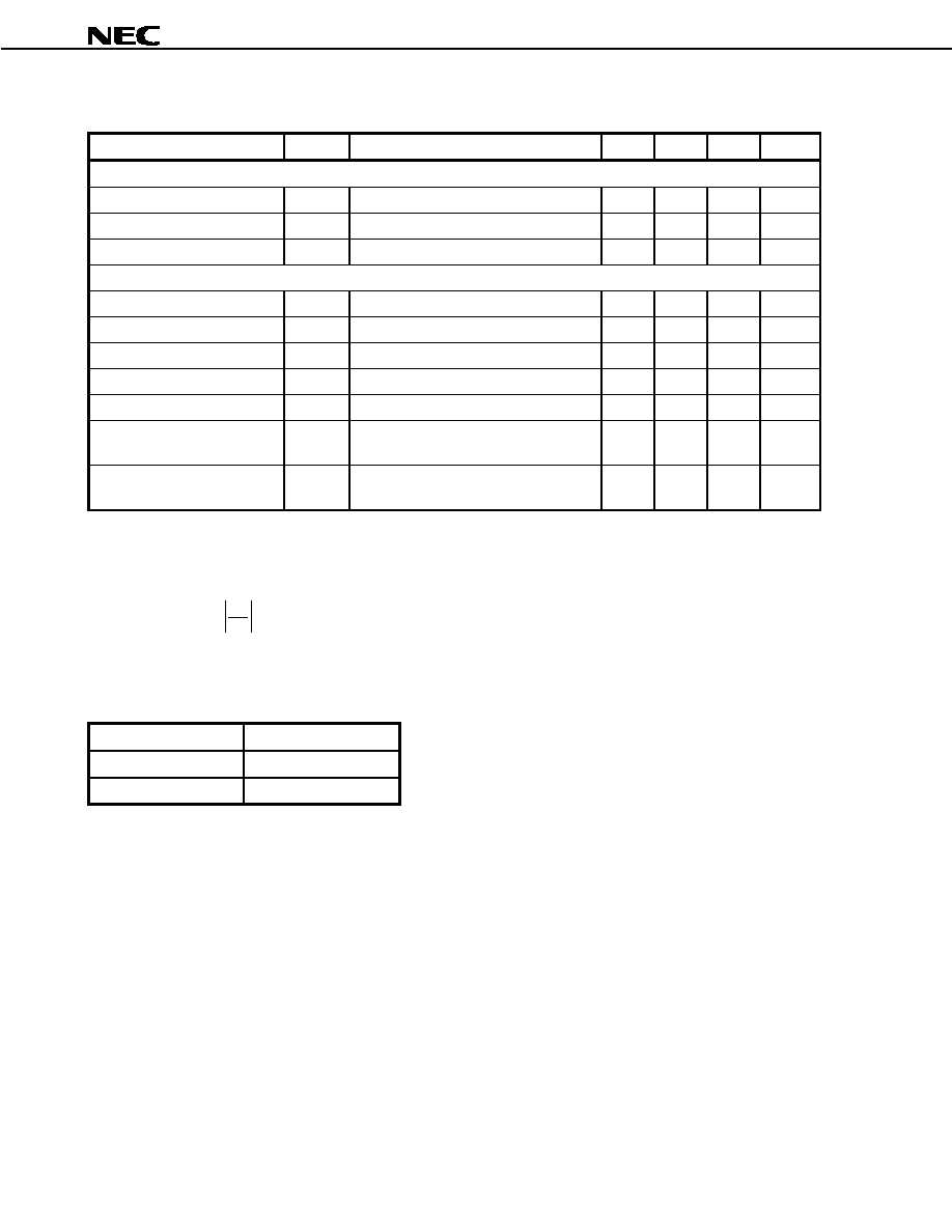
ABSOLUTE MAXIMUM RATINGS
Parameter
Symbol
Ratings
Unit
Collector to Base Voltage
V
CBO
15
V
Collector to Emitter Voltage
V
CEO
3.3
V
Emitter to Base Voltage
V
EBO
1.5
V
Collector Current
I
C
12
mA
Total Power Dissipation
P
tot
Note
39
mW
Junction Temperature
T
j
150
∞C
Storage Temperature
T
stg
≠65 to +150
∞C
Note T
A
= +25 ∞C (free air)
THERMAL RESISTANCE
Item
Symbol
Value
Unit
Junction to Case Resistance
R
th j-c
240
∞C/W
Junction to Ambient Resistance
R
th j-a
650
∞C/W
Because this product uses high-frequency technology, avoid excessive static electricity, etc.
Preliminary Data Sheet P13864EJ1V0DS00
2
2SC5507
ELECTRICAL CHARACTERISTICS (T
A
= +25 ∞C)
Parameter
Symbol
Test Conditions
MIN.
TYP.
MAX.
Unit
DC characteristics
Collector Cut-off Current
I
CBO
V
CB
= 5 V, I
E
= 0
≠
≠
100
nA
Emitter Cut-off Current
I
EBO
V
EB
= 1 V, I
C
= 0
≠
≠
100
nA
DC Current Gain
h
FE
Note 1
V
CE
= 2 V, I
C
= 5 mA
50
70
100
≠
RF Characteristics
Reverse Transfer Capacitance
C
re
Note 2
V
CB
= 2 V, I
E
= 0, f = 1 MHz
≠
0.08
0.12
pF
Gain Bandwidth Product
f
T
V
CE
= 3 V, I
C
= 10 mA, f = 2 GHz
20
25
≠
GHz
Noise Figure
NF
V
CE
= 2 V, I
C
= 2 mA, f = 2 GHz, Z
S
= Z
opt
≠
1.2
1.5
dB
Insertion Power Gain
|
S
21e
|
2
V
CE
= 2 V, I
C
= 5 mA, f = 2 GHz
14
17
≠
dB
Maximum Stable Power Gain
MSG
Note 3
V
CE
= 2 V, I
C
= 5 mA, f = 2 GHz
≠
22
≠
dB
Output Power at 1 dB
Compression Point
P
-1
V
CE
= 2 V, I
C
= 5 mA
Note 4
, f = 2 GHz
≠
5
≠
dBm
Output Power at Third Order
Intercept Point
OIP
3
V
CE
= 2 V, I
C
= 5 mA
Note 4
, f = 2 GHz
≠
15
≠
≠
Notes 1. Pulse measurement PW
350
µ
s, Duty cycle
2%
2. Emitter to base capacitance measured using capacitance meter (self-balancing bridge method) when
the emitter is connected to the guard pin
3.
S
21
MSG =
S
12
4. Collector current when P
-1
is output
h
FE
CLASSIFICATION
Rank
FB
Marking
T78
h
FE
50 to 100
Preliminary Data Sheet P13864EJ1V0DS00
3
2SC5507
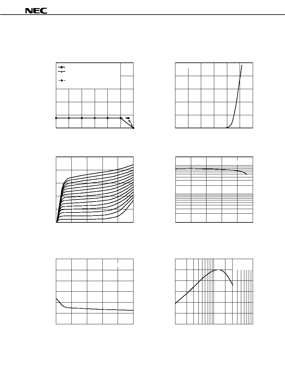
TYPICAL CHARACTERISTICS (T
A
= +25 ∞C)
Thermal/DC Characteristics
Collector Current vs. Collector to Emitter Voltage
DC Current Gain vs. Collector Current
0.001
200
100
10
25
20
15
10
5
0
1
2
3
4
5
1
0.01
0.1
1
10
100
Collector to Emitter Voltage V
CE
(V)
Collector Current I
C
(mA)
Collector Current I
C
(mA)
DC Current Gain h
FE
Total Power Dissipation vs.
Ambient Temperature, Case Temperature
Collector Current vs. DC Base Voltage
50
40
30
20
10
250
200
150
100
50
0
Ambient Temperature T
A
(
∞
C), Case Temperature T
C
(
∞
C)
DC Base Voltage V
BE
(V)
Total Power Dissipation P
T
(mW)
Collector Current I
C
(mA)
P
T
-T
A
: Free air
P
T
-T
A
: Mounted on ceramic board
(15 mm
◊
15 mm, t = 0.6 mm)
P
T
-T
C
: When case temperature
is specified
0
25
50
75
100
125
150
0
0.2
0.4
0.6
0.8
1.0
1.2
300 A
280 A
260 A
240 A
220 A
200 A
180 A
160 A
140 A
120 A
100 A
80 A
60 A
40 A
µ
µ
µ
µ
µ
µ
µ
µ
µ
µ
µ
µ
µ
µ
µ
µ
I
B
= 20 A
V
CE
= 2 V
V
CE
= 2 V
Capacitance/f
T
Characteristics
1
0.30
0.25
0.20
0.15
0.10
0.05
0
1.0
2.0
3.0
4.0
5.0
30
25
20
15
10
5
0
10
100
Gain Bandwidth Product vs. Collector Current
Reverse Transfer Capacitance vs. Collector to Base Voltage
Reverse Transfer Capacitance C
re
(pF)
Collector to Base Voltage V
CB
(V)
Gain Bandwidth Product f
T
(GHz)
Collector Current I
C
(mA)
f = 1 MHz
V
CE
= 3 V
f = 2 GHz
Preliminary Data Sheet P13864EJ1V0DS00
4
2SC5507
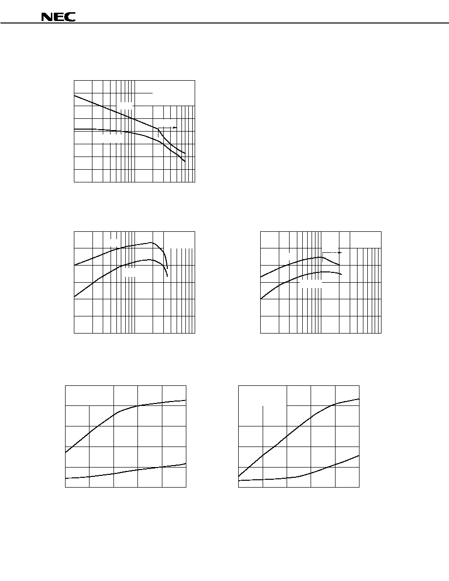
Gain Characteristics
Collector Current I
C
(mA)
Collector Current I
C
(mA)
Insertion Power Gain, Maximum Available Power Gain,
Maximum Stable Power Gain vs. Frequency
Insertion Power Gain, Maximum Stable Power Gain
vs. Collector Current
Insertion Power Gain, Maximum Available Power Gain,
Maximum Stable Power Gain vs. Collector Current
40
35
30
25
20
15
10
5
0
30
25
20
15
10
5
0
30
25
20
15
10
5
0
Frequency f (GHz)
Insertion Power Gain |S
21e
|
2
(dB)
Maximum Available Power Gain MAG (dB)
Maximum Stable Power Gain MSG (dB)
Insertion Power Gain
|S
21e
|
2
(dB)
Maximum Stable Power Gain MSG (dB)
Insertion Power Gain |S
21e
|
2
(dB)
Maximum Available Power Gain MAG (dB)
Maximum Stable Power Gain MSG (dB)
0.1
1.0
10.0
1
10
100
1
10
100
MAG
MSG
|S
21e
|
2
V
CE
= 2 V
I
C
= 5 mA
MSG
|S
21e
|
2
MSG
|S
21e
|
2
MAG
f = 2 GHz
V
CE
= 2 V
f = 1 GHz
V
CE
= 2 V
Output Characteristics
Input Power P
in
(dBm)
Output Power, Collector Current vs. Input Power
10
5
0
≠5
≠10
≠15
25
20
15
10
5
0
25
20
15
10
5
0
Output Power P
out
(dBm)
Collector Current I
C
(mA)
≠30
≠25
≠20
≠15
≠10
≠5
P
out
I
C
f = 1 GHz
V
CE
= 2 V
Input Power P
in
(dBm)
Output Power, Collector Current vs. Input Power
10
5
0
≠5
≠10
≠15
Output Power P
out
(dBm)
Collector Current I
C
(mA)
≠30
≠25
≠20
≠15
≠10
≠5
P
out
I
C
f = 2 GHz
V
CE
= 2 V
Preliminary Data Sheet P13864EJ1V0DS00
5
2SC5507
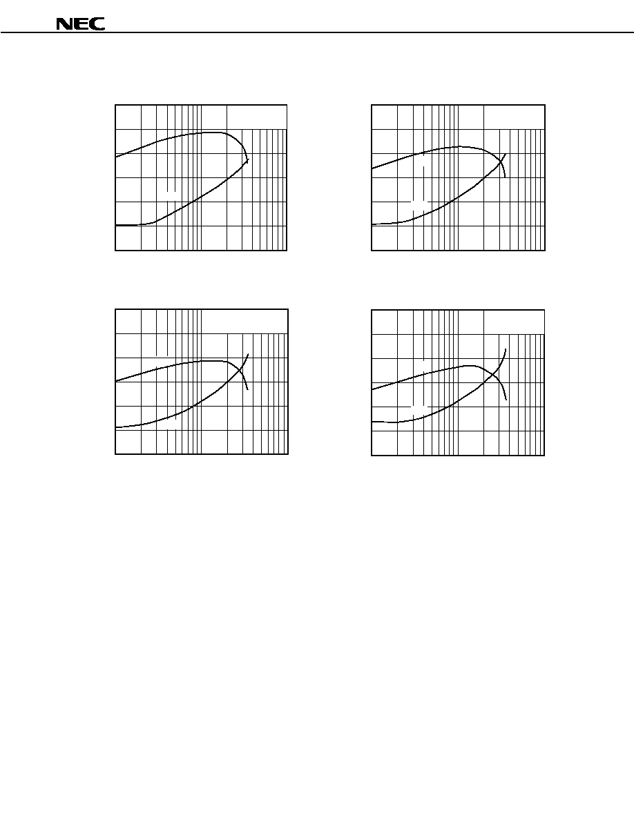
Noise Characteristics
Noise Figure, Associated Gain vs. Collector Current
Noise Figure, Associated Gain vs. Collector Current
Noise Figure, Associated Gain vs. Collector Current
Noise Figure, Associated Gain vs. Collector Current
Collector Current I
C
(mA)
Collector Current I
C
(mA)
6
5
4
3
2
1
0
Collector Current I
C
(mA)
Collector Current I
C
(mA)
Noise Figure NF (dB)
Associated Gain G
a
(dB)
Associated Gain G
a
(dB)
Noise Figure NF (dB)
1
10
100
6
5
4
3
2
1
0
30
25
20
15
10
5
0
1
10
100
1
10
100
1
10
100
G
a
f = 2.5 GHz
V
CE
= 2 V
NF
G
a
f = 1.5 GHz
V
CE
= 2 V
NF
30
25
20
15
10
5
0
6
5
4
3
2
1
0
Noise Figure NF (dB)
Associated Gain G
a
(dB)
Associated Gain G
a
(dB)
Noise Figure NF (dB)
6
5
4
3
2
1
0
30
25
20
15
10
5
0
30
25
20
15
10
5
0
G
a
f = 2.0 GHz
V
CE
= 2 V
NF
G
a
f = 1.0 GHz
V
CE
= 2 V
NF