 | –≠–ª–µ–∫—Ç—Ä–æ–Ω–Ω—ã–π –∫–æ–º–ø–æ–Ω–µ–Ω—Ç: D16805 | –°–∫–∞—á–∞—Ç—å:  PDF PDF  ZIP ZIP |
Document Outline
- COVER
- DESCRIPTION
- FEATURES
- ORDERING INFORMATION
- BLOCK DIAGRAM
- ABSOLUTE MAXIMUM RATINGS
- RECOMMENDED OPERATING CONDITIONS
- ELECTRICAL SPECIFICATIONS (Unless otherwise specified, TA = 25 degree, VDD = recommended, operating condition, VM = 0.5 to 7.5 V
- FUNCTION TABLE
- APPLICATION CIRCUIT 1
- APPLICATION CIRCUIT 2
- TYPICAL CHARACTERISTICS (TA = 25 degree)
- PACKAGE DIMENSION
- RECOMMENDED SOLDERING CONDITIONS

©
1997
DATA SHEET
MOS INTEGRATED CIRCUIT
µ
PD16805
MONOLITHIC H BRIDGE DRIVER CIRCUIT
DESCRIPTION
The
µ
PD16805 is a monolithic H bridge driver IC which uses low-ON resistance power MOS FETs in its driver stage.
This driver has a forward, reverse, and brake functions and is ideal for the driver circuit of motors for camera that
advance or rewind the film, and for auto focusing or zooming.
This IC supports a drive current of up to 1.0 A (DC).
FEATURES
PIN CONFIGURATION (Top View)
∑
High drive current
I
DR
= 4.2 A MAX. at PW
200 ms (single pulse)
I
DR
= 1.0 A (DC)
∑
Low-ON resistance (sum of ON resistances of top
and bottom MOS FET)
R
ON
= 0.4
TYP. at I
DR
= 1.0 A
∑
Standby function that turns OFF charge pump circuit
∑
Compact surface mount package
16-pin plastic SOP (300 mil)
ORDERING INFORMATION
Part Number
Package
µ
PD16805GS
16-pin plastic SOP (300 mil)
BLOCK DIAGRAM
C
1
V
DD
V
G
V
M
OUT1
OUT2
PGND
DGND
C
2
C
3
IN2
IN1
INC
STBY
Contorol
circuit
Contorol
circuit
Level shift
circuit
D MOS FET
H bridge circuit
Charge pump
circuit
50 k
C
1
= C
2
= C
3
: External capacitors (10 nF)
Load motor
Document No. G11032EJ3V0DS00 (3rd edition)
Date Published July 1997 N
Printed in Japan
The information in this document is subject to change without notice.
C
2L
16
C
1H
15
C
1L
14
V
M
13
V
DD
12
IN
1
11
IN
2
10
INC
9
1
2
3
4
5
6
7
8
C
2H
V
G
STBY
OUT2
PGND
OUT1
V
M
DGND

µ
PD16805
2
ABSOLUTE MAXIMUM RATINGS
Parameter
Symbol
Conditions
Rating
Unit
Supply voltage
V
DD
≠0.5 to +6.5/+8.0
Note
V
V
M
≠0.5 to +6.5/+8.0
Note
V
G
pin applied voltage
V
G
15
V
Input voltage
V
IN
≠0.5 to V
DD
+ 0.5
V
H bridge drive current
I
DR1
DC
1.0
A
I
DR2
PW
200 ms (single pulse)
4.2
A
Power consumption
P
T
T
A
= 25
∞
C
1.0
W
Operating temperature range
T
A
≠30 to +60
∞
C
Operating junction temperature
T
J (MAX)
150
∞
C
Storage temperature range
T
stg
≠55 to +150
∞
C
Note V
DD
when the charge pump is used/V
DD
and V
M
when V
G
is supplied from an external source
RECOMMENDED OPERATING CONDITIONS
Parameter
Symbol
Conditions
Ratings
Unit
MIN.
TYP.
MAX.
Supply voltage
V
DD
During normal operation
3.0
6.0/7.5
Note 2
V
All input pins are low
2.5
V
M
0.5
7.5
V
Charge pump capacitance
C
1
to C
3
10
nF
V
G
pin applied voltage
Note 1
V
G
11
14
V
Operating temperature
T
A
Ambient temperature
≠30
60
∞
C
Notes 1. When a voltage is applied from an external source to the V
G
pin
2. When the charge pump is used/when V
G
is supplied from an external source
µ
PD16805
3
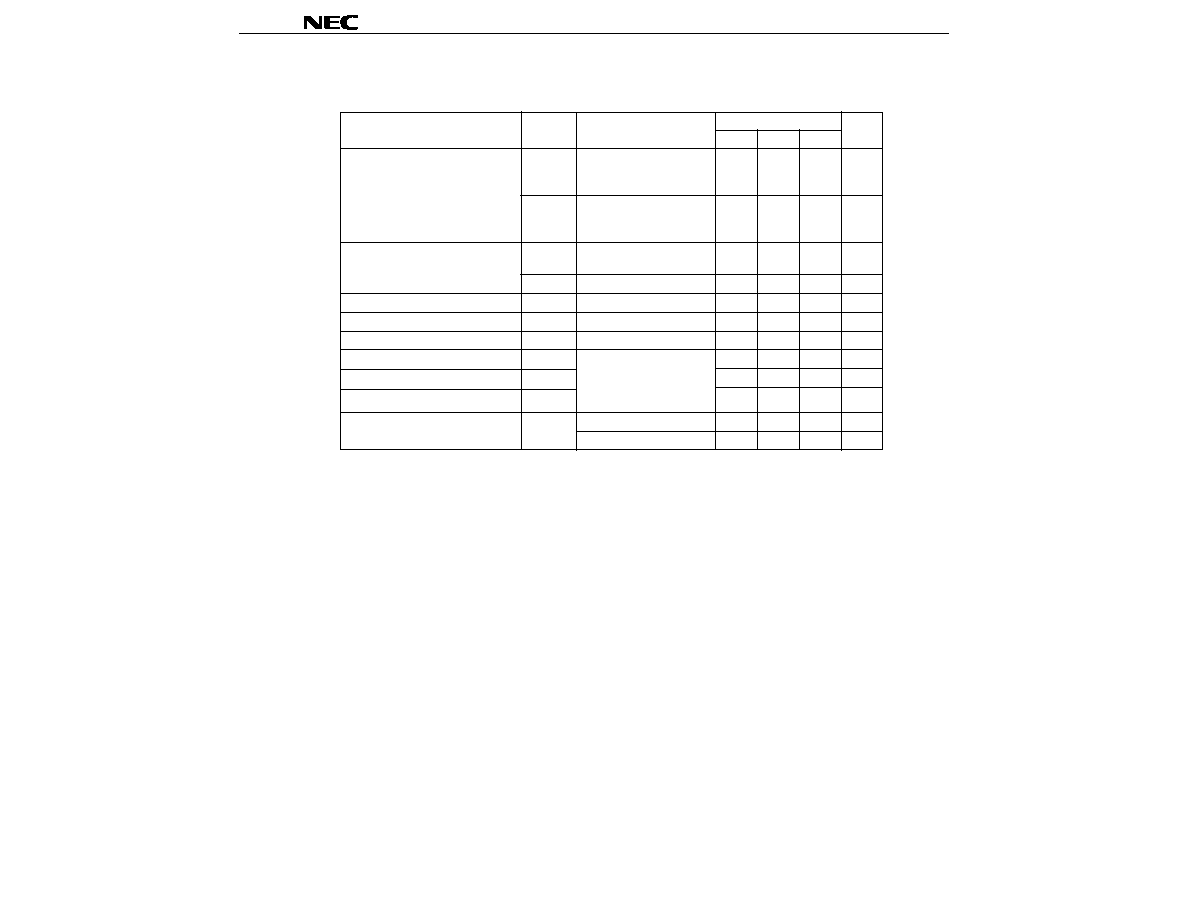
ELECTRICAL SPECIFICATIONS (Unless otherwise specified, T
A
= 25
∞
C, V
DD
= recommended
operating condition, V
M
= 0.5 to 7.5 V)
Parameter
Symbol
Conditions
Ratings
Unit
MIN.
TYP.
MAX.
V
DD
pin current
I
DD1
V
DD
= 5 V, T
A
= recommended
0.6
2.0
mA
conditions
Control pins at high level
I
DD2
V
DD
= 5 V, T
A
= recommended
0.3
10
µ
A
conditions
Control pins at low level
V
M
pin current
I
M1
Control pins at low level,
0.1
10
µ
A
T
A
= recommended conditions
I
M2
Control pins at low level
1.0
µ
A
H bridge ON resistance
Note
R
ON
I
DR
= 1.0 A, V
DD
= V
M
= 5 V
0.4
0.6
Control pin high-level input voltage
V
IH
T
A
= recommended condition
V
DD
◊
0.6
V
Control pin low-level input voltage
V
IL
T
A
= recommended condition
V
DD
◊
0.2
V
Charge pump circuit turn-ON time
t
ONG
V
DD
= V
M
= 5 V,
0.5
1.0
ms
H bridge output circuit turn-ON time
t
ONH
T
A
= recommended conditions
10
µ
s
H bridge output circuit turn-OFF time
t
OFFH
C
1
= C
2
= C
3
= 10 nF
5.0
µ
s
I
DR
= 1.0 A
Control pin input pull-down resistor
R
IND
35
50
65
k
T
A
= recommended condition
25
75
k
Note Sum of ON resistances of top and bottom MOS FETs

µ
PD16805
4
FUNCTION TABLE
Input Signal
Function
IN1
IN2
INC
STB
H
L
H
H
Forward mode
L
H
H
H
Reverse mode
H
H
H
H
Brake mode
L
L
H
H
Stop mode
◊
◊
L
H
Stop mode
◊
◊
◊
L
Standby mode
V
M
ON
OFF
ON
OFF
OUT1
OUT2
V
M
ON
OFF
ON
OFF
OUT1
OUT2
V
M
ON
OFF
ON
OFF
OUT1
OUT2
V
M
OFF
OFF
OFF
OFF
OUT1
OUT2
Forward mode
Reverse mode
Brake mode
Stop mode

µ
PD16805
5
APPLICATION CIRCUIT 1
Note It is recommended to connect a capacitor of 1 to 10
µ
F between V
M
and GND to protect the gate of the
DMOS FET from surge voltage.
V
M
= 0.5 V to 7.5 V
V
DD
= 3.0 V to 6.0 V
C
1
= C
2
= C
3
= 10 = nF
C
1
C
2
C
3
V
DD
5
V
M
OUT1
OUT2
PGND
V
M
10
2
3
16
1
15
4
11
13
12
DGND
INC
STBY 14
8
6
7
IN1
IN2
9
M
OSC
circuit
Charge pump circuit
Control circuit
Level shift
circuit
D MOS FET
H bridge
circuit
Battery
CPU
Pull-down resistor
50 k
TYP.
Film
take-up motor
Forward
mode
Brake
mode
Reverse
mode
Stop mode
DC-DC
convertor
C
4
Note
1 to 10 F
H
H
L
L
IN
1
µ
IN
2