 | –≠–ª–µ–∫—Ç—Ä–æ–Ω–Ω—ã–π –∫–æ–º–ø–æ–Ω–µ–Ω—Ç: NE321000 | –°–∫–∞—á–∞—Ç—å:  PDF PDF  ZIP ZIP |

The information in this document is subject to change without notice. Before using this document, please
confirm that this is the latest version.
Not all devices/types available in every country. Please check with local NEC representative for
availability and additional information.
HETERO JUNCTION FIELDEFFECT TRANSISTOR
NE321000
C to Ka BAND SUPER LOW NOISE AMPLIFIER
N-CHANNEL HJ-FET CHIP
Document No. P14270EJ2V0DS00 (2nd edition)
Date Published November 1999 N CP(K)
Printed in Japan
DATA SHEET
1999
©
The mark shows major revised points.
DESCRIPTION
The NE321000 is Hetero Junction FET that utilizes the hetero junction to create high mobility electrons. Its
excellent low noise and associated gain make it suitable for DBS and another commercial systems, industrial and
space applications.
FEATURES
∑
Super Low Noise Figure & High Associated Gain
NF = 0.35 dB TYP. G
a
= 13.5 dB TYP. @ f = 12 GHz
∑
Gate Length: L
g
0.20
µ
m
∑
Gate Width : W
g
= 160
µ
m
ORDERING INFORMATION (PLAN)
Part Number
Quality Grade
NE321000
Standard (Grade D)
Remark To order evaluation samples, please contact your local NEC sales office. (Part number for sample order:
NE321000)
ABSOLUTE MAXIMUM RATINGS (T
A
= +25∞C)
Parameter
Symbol
Ratings
Unit
Drain to Source Voltage
V
DS
4.0
V
Gate to Source Voltage
V
GS
≠3.0
V
Drain Current
I
D
I
DSS
mA
Gate Current
I
G
100
µ
A
Total Power Dissipation
P
tot
Note
200
mW
Channel Temperature
T
ch
175
∞C
Storage Temperature
T
stg
≠65 to +175
∞C
Note Chip mounted on an Alumina heatsink (size: 3
◊
3
◊
0.6 t)

Data Sheet P14270EJ2V0DS00
2
NE321000
RECOMMENDED OPERATING CONDITIONS (T
A
= +25 ∞C)
Parameter
Symbol
MIN.
TYP.
MAX.
Unit
Drain to Source Voltage
V
DS
1
2
3
V
Drain Current
I
D
5
10
15
mA
Input Power
P
in
≠
≠
0
dBm
ELECTRICAL CHARACTERISTICS (T
A
= +25 ∞C)
Parameter
Symbol
Test Conditions
MIN.
TYP.
MAX.
Unit
Gate to Source Leak Current
I
GSO
V
GS
= ≠3 V
≠
0.5
10
µ
A
Saturated Drain Current
I
DSS
V
DS
= 2 V, V
GS
= 0 V
15
40
70
mA
Gate to Source Cut Off Voltage
V
GS(off)
V
DS
= 2 V, I
DS
= 100
µ
A
≠0.2
≠0.7
≠2.0
V
Transconductance
g
m
V
DS
= 2 V, I
DS
= 10 mA
40
55
≠
mS
Noise Figure
NF
≠
0.35
0.45
dB
NF Associated Gain
G
a
V
DS
= 2 V, I
DS
= 10 mA
f = 12 GHz
12.0
13.5
≠
dB
Remark RF performance is determined by packaging and testing 10 chips per wafer.
Wafer rejection criteria for standard devices is 2 rejects per 10 samples.

Data Sheet P14270EJ2V0DS00
3
NE321000
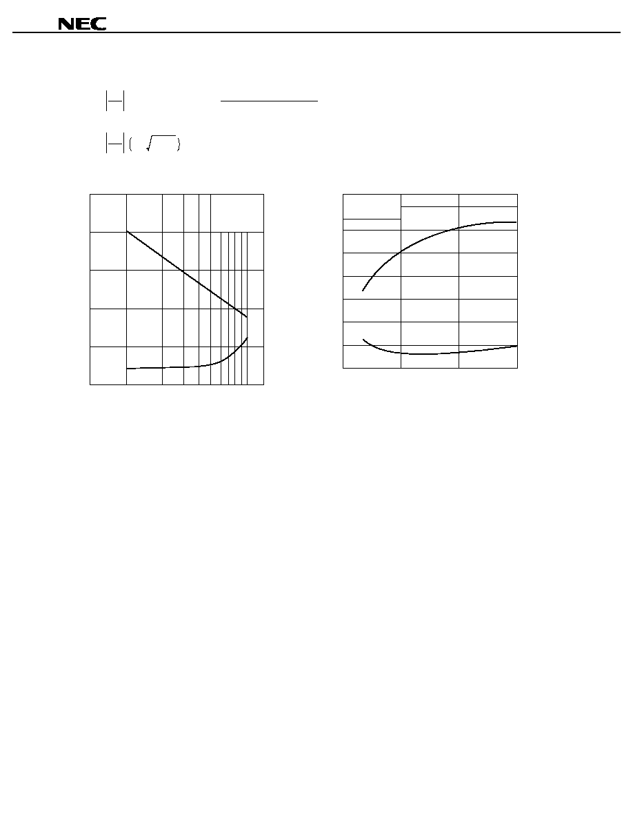
TYPICAL CHARACTERISTICS (T
A
= +25 ∞C)
250
200
150
100
50
0
50
100
150
200
250
TOTAL POWER DISSIPATION vs.
AMBIENT TEMPERATURE
Ambient Temperature T
A
(
∞
C)
Total Power Dissipation P
tot
(mW)
DRAIN CURRENT vs.
DRAIN TO SOURCE VOLTAGE
Drain to Source Voltage V
DS
(V)
100
80
60
40
20
0
2.0
1.0
Drain Current I
D
(mA)
V
GS
= 0 V
≠0.2 V
≠0.4 V
≠0.6 V
60
40
20
0
≠2.0
≠1.0
0
DRAIN CURRENT vs.
GATE TO SOURCE VOLTAGE
Gate to Source Voltage V
GS
(V)
Drain Current I
D
(mA)
Frequency f (GHz)
Maximum Stable Gain MSG. (dB)
Maximum Available Gain MAG. (dB)
Forward Insertion Gain |S
21s
|
2
(dB)
V
DS
= 2 V
MAXIMUM AVAILABLE GAIN, FORWARD
INSERTION GAIN vs. FREQUENCY
24
20
16
12
8
4
1
30
2
4
20
6
8 10
14
V
DS
= 2 V
I
D
= 10 mA
MSG.
|S
21S
|
2
Data Sheet P14270EJ2V0DS00
4
NE321000
GAIN CALCULATIONS
S
21
MAG. =
S
12
k
±
k
2
≠ 1
= S
11
∑S
22
≠ S
21
∑S
12
S
21
MSG. =
S
12
1 + |
|
2
≠ |S
11
|
2
≠ |S
22
|
2
K =
2 |S
12
| |S
21
|
Frequency f (GHz)
1.0
0.5
0
1
30
2
Noise Figure NF (dB)
V
DS
= 2 V
I
D
= 10 mA
4
20
6
8 10
14
24
20
16
12
8
4
NF Associated Gain G
a
(dB)
Noise Figure NF (dB)
NF Associated Gain G
a
(dB)
Drain Current I
D
(mA)
G
a
NF
G
a
NF
NOISE FIGURE, NF ASSOCIATED GAIN vs.
DRAIN CURRENT
15
14
13
12
11
2.0
1.5
1.0
0.5
30
20
10
0
V
DS
= 2 V
f = 12 GHz
NOISE FIGURE, NF ASSOCIATED GAIN vs.
FREQUENCY

Data Sheet P14270EJ2V0DS00
5
NE321000
S-PARAMETERS
MAG. AND ANG.
V
DS
= 2 V, I
D
= 10 mA
FREQUENCY
S
11
S
21
S
12
S
22
GHz
MAG.
ANG.
MAG.
ANG.
MAG.
ANG.
MAG.
ANG.
2.0
3.0
4.0
5.0
6.0
7.0
8.0
9.0
10.0
11.0
12.0
13.0
14.0
15.0
16.0
17.0
18.0
19.0
20.0
21.0
22.0
23.0
24.0
25.0
26.0
27.0
28.0
29.0
30.0
0.998
0.987
0.981
0.970
0.962
0.952
0.941
0.927
0.912
0.898
0.882
0.868
0.855
0.843
0.827
0.807
0.796
0.793
0.788
0.782
0.783
0.785
0.778
0.766
0.757
0.753
0.755
0.748
0.743
-
13.2
-
19.3
-
25.7
-
32.7
-
38.6
-
44.4
-
50.1
-
55.6
-
61.5
-
66.9
-
71.6
-
75.9
-
80.2
-
84.2
-
88.5
-
92.6
-
95.3
-
98.0
-
101.2
-
103.8
-
106.4
-
109.9
-
113.4
-
116.0
-
118.1
-
119.9
-
121.6
-
124.2
-
126.2
4.72
4.70
4.62
4.50
4.45
4.37
4.28
4.17
4.03
3.90
3.79
3.66
3.54
3.42
3.30
3.16
3.05
2.97
2.89
2.79
2.70
2.62
2.53
2.46
2.40
2.33
2.29
2.23
2.16
170.2
165.6
160.5
155.7
151.6
147.4
143.5
139.7
135.6
131.5
128.0
124.9
121.9
119.0
115.8
112.9
110.8
108.7
106.2
104.1
101.9
99.5
97.4
95.8
93.8
92.5
90.6
88.4
86.8
0.020
0.030
0.040
0.050
0.059
0.067
0.074
0.081
0.087
0.094
0.100
0.104
0.108
0.111
0.115
0.116
0.117
0.120
0.123
0.125
0.128
0.132
0.135
0.135
0.135
0.133
0.136
0.135
0.136
81.3
77.3
73.2
69.4
65.3
62.2
58.6
55.2
51.5
48.0
44.9
42.0
39.0
36.2
33.5
30.5
28.5
27.9
26.5
24.9
23.3
20.7
18.8
16.8
15.3
14.3
14.0
12.6
11.3
0.602
0.599
0.593
0.588
0.583
0.574
0.567
0.564
0.552
0.541
0.536
0.526
0.518
0.509
0.501
0.494
0.488
0.489
0.487
0.484
0.486
0.477
0.474
0.481
0.469
0.463
0.484
0.481
0.475
-
10.0
-
14.8
-
19.9
-
25.6
-
30.1
-
34.4
-
39.1
-
43.1
-
47.2
-
52.0
-
55.5
-
58.6
-
62.1
-
65.0
-
68.3
-
71.2
-
73.2
-
75.2
-
77.4
-
80.9
-
82.7
-
84.1
-
87.9
-
88.3
-
89.2
-
91.6
-
93.5
-
95.2
-
97.5