 | –≠–ª–µ–∫—Ç—Ä–æ–Ω–Ω—ã–π –∫–æ–º–ø–æ–Ω–µ–Ω—Ç: NE8500100 | –°–∫–∞—á–∞—Ç—å:  PDF PDF  ZIP ZIP |
©
1996
PRELIMINARY DATA SHEET
GaAs MES FET
NE85001 SERIES
1 W C-BAND POWER GaAs FET
N-CHANNEL GaAs MES FET
Document No. P10968EJ1V0DS00 (1st edition)
Date Published June 1996 P
Printed in Japan
DESCRIPTION
The NE8500199 Power GaAs FET covers 2 GHz to 10 GHz frequency range for commercial amplifier, oscillator
applications and so on.
NE8500100 is the two-cells recessed gate chip used in `99' package.
The device incorporates Ti-Al gate and silicon dioxide glassivation. To reduce the thermal resistance, the device
has a PHS. (Plated Heat Sink)
NEC's strigent quality assurance and test procedures assure the highest reliability and performance.
FEATURES
∑
Class A operation
∑
High power output
∑
High reliability
SELECTION CHART
PERFORMANCE SPECIFIED
PART NUMBER
FORM
Pout (**)
G
L
(**)
USABLE
(dBm)
(dB)
FREQUENCY
(GHz)
NE8500100(*)
chip
28.5 min
9.0 typ
2.0 to 10
NE8500100-WB
NE8500100-RG
NE8500199
package
28.5 min
9.0 typ
2.0 to 10
*
WB, RG indicate a type of containers for chips.
WB: black carrier, RG: ring,: gel-pack,
** Specified at the condition at the last page.
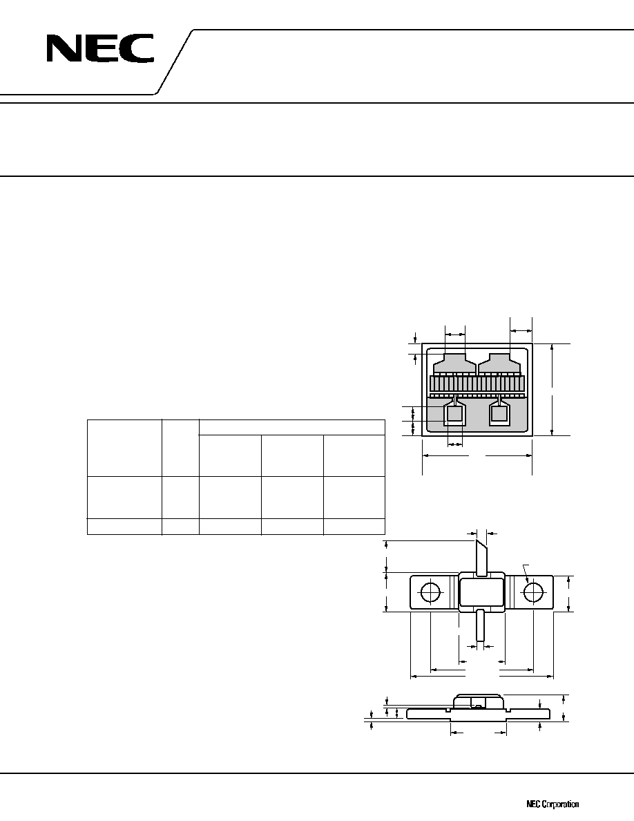
PHYSICAL DIMENSIONS
NE8500100 (CHIP) (unit:
µ
m)
PACKAGE CODE-99 (unit: mm)
4.0 MIN BOTH LEADS
SOURCE
GATE
DRAIN
0.6 ±0.1
5.2 ±0.3
6.0 ±0.2
11.0 ±0.3
15.0 ±0.3
0.1
1.2
0.2 MAX.
1.0 ±0.1
2.2 ±0.3
2 PLACES
4.3 ±0.2
1.7 ±0.15
4.0
5.0 MAX.
780
640
170
100
146
100
65
100

NE85001 SERIES
2
ABSOLUTE MAXIMUM RATINGS (T
A
= 25 ∞C)
Drain to Source Voltage
V
DSX
15
V
Gate to Drain Voltage
V
GDX
≠18
V
Gate to Source Voltage
V
GSX
≠12
V
Total Power Disipation(*)
P
T
6.0
W
Drain Current
I
D
1.12
A
Gate Current
I
G
6.0
mA
Channel Temperature
T
ch
175
∞C
Storage Temperature
T
stg
≠65 to 175
∞C
*T
C
= 25 ∞C
RECOMMENDING OPERATION RANDGE
CHARACTERISTIC
SYMBOL
MIN.
TYP.
MAX.
UNIT
Drain to Source Voltage
V
DS
9
≠
10
V
Channel Temperature
T
ch
≠
≠
130
∞C
Input Power
Gcomp
≠
≠
3
dBcomp
Gate Resistance
Rg
≠
≠
1
k
ELECTRICAL CHARACTERISTICS (T
A
= 25 ∞C)
CHARACTERISTIC
SYMBOL
MIN.
TYP.
MAX.
UNIT
TEST CONDITIONS
Saturated Drain Current
Idss
430
≠
860
mA
Vds = 2.5 V, Vgs = 0 V
Pinch-off Voltage
V
P
≠3.0
≠
≠1.0
V
Vds = 2.5 V, Ids = 4 mA
Transconductance
gm
≠
300
≠
mS
Vds = 2.5 V, Ids = Idss
Thermal Resistance
R
th
≠
≠
30
∞C/W
PERFORMANCE SPECIFICATIONS (T
A
= 25 ∞C)
PART NUMBER
PACKAGE CODE
CHARACTERISTIC
SYMBOL
Output Power
P
O
Gate to source
Igs
Current
Linear Gain
G
L
*
Pin for Pout specification.
** The same conditions as the above except this.
NE8500100
NE8500100-WG
NE8500100-RG
CHIP
MIN.
TYP.
MAX.
28.5
≠
≠
≠2.0
≠
2.0
≠
9
≠
NE8500199
99
MIN.
TYP.
MAX.
28.5
≠
≠
≠2.0
≠
2.0
≠
9
≠
UNIT
dBm
mA
dB
TEST CONDITIONS
Pin
11 dBm (**)
f = 7.2 GHz
Vds = 10 V
Ids = 200 mA set
Rg = 1 k
Pin = 21.0 dBm(*)

NE85001 SERIES
3
TYPICAL CHARACTERISTICS (T
A
= 25 ∞C)
NE8500199
OUTPUT POWER vs. INPUT POWER
P
out
- Output Power - dBm
10
P
in
- Input Power - dBm
25
20
15
30
15
20
300
250
200
I
D
(mA)
V
DS
= 10 V
I
ds
= 200 mA set
f = 7.2 GHz

NE85001 SERIES
4
S-PARAMETER
V
DS
= 10 V, I
DS
= 200 mA, V
GS
= ≠1.260 V, I
G
= 0.0 mA, R
G
= 1 k
FREQUENCY
S
11
S
21
S
12
S
22
GHz
MAG
ANG
MAG
ANG
MAG
ANG
MAG
ANG
0.100
0.990
≠22.7
14.418
165.5
0.007
70.1
0.065
≠64.6
0.500
0.916
≠91.1
10.211
123.3
0.024
47.7
0.175
≠126.4
1.000
0.869
≠132.1
6.444
94.8
0.031
33.6
0.221
≠149.1
1.500
0.851
≠152.9
4.610
76.6
0.034
29.0
0.241
≠159.2
2.000
0.840
≠166.1
3.591
61.9
0.038
28.1
0.260
≠165.6
2.500
0.831
≠175.9
2.975
49.1
0.042
26.7
0.278
≠170.8
3.000
0.826
176.0
2.601
37.3
0.047
25.4
0.296
≠174.6
3.500
0.824
168.8
2.341
26.0
0.053
27.4
0.313
≠177.8
3.600
0.825
167.5
2.291
23.4
0.055
27.0
0.317
≠179.2
3.700
0.825
166.0
2.253
20.7
0.056
26.5
0.323
179.8
3.800
0.827
164.4
2.230
18.1
0.059
26.8
0.333
179.4
3.900
0.829
162.8
2.187
16.1
0.063
26.5
0.340
178.7
4.000
0.829
161.0
2.127
13.4
0.066
25.4
0.345
176.3
4.200
0.821
157.2
2.053
8.6
0.072
20.1
0.353
171.0
4.400
0.808
153.9
1.976
5.6
0.074
16.8
0.343
167.3
4.500
0.803
152.5
1.963
3.4
0.075
15.2
0.337
166.2
4.600
0.799
151.0
1.970
0.8
0.077
13.9
0.340
164.8
4.800
0.790
147.9
1.944
≠3.1
0.080
12.6
0.341
163.2
5.000
0.784
144.7
1.929
≠8.6
0.084
9.3
0.340
159.8
5.200
0.777
141.4
1.923
≠12.8
0.089
7.4
0.349
158.6
5.400
0.771
137.7
1.897
≠18.5
0.093
4.5
0.347
155.6
5.500
0.767
135.9
1.916
≠20.7
0.097
3.1
0.358
154.2
5.600
0.764
133.9
1.916
≠22.7
0.100
1.8
0.363
154.5
5.800
0.758
130.1
1.887
≠28.5
0.105
≠1.9
0.358
151.6
6.000
0.751
125.8
1.928
≠33.5
0.113
≠4.8
0.381
149.5
6.200
0.742
121.3
1.896
≠39.1
0.116
≠8.0
0.369
146.8
6.400
0.731
116.6
1.951
≠44.8
0.126
≠11.6
0.397
144.2
6.500
0.726
114.1
1.951
≠47.2
0.130
≠13.2
0.396
144.2
6.600
0.721
111.6
1.936
≠50.6
0.133
≠15.9
0.387
141.8
6.800
0.707
106.1
1.973
≠56.8
0.143
≠20.4
0.411
138.6
7.000
0.689
100.2
1.957
≠62.4
0.149
≠23.9
0.402
137.1
7.200
0.676
93.9
2.004
≠69.1
0.163
≠28.9
0.424
133.8
7.400
0.657
87.1
2.002
≠74.9
0.171
≠33.3
0.425
132.3
7.500
0.649
83.4
2.013
≠78.8
0.177
≠36.8
0.431
129.4
7.600
0.640
79.9
2.045
≠82.4
0.185
≠39.6
0.448
127.2
7.800
0.621
71.8
2.042
≠88.6
0.195
≠45.0
0.452
123.8
8.000
0.604
63.2
2.067
≠96.6
0.206
≠51.8
0.465
117.2
8.200
0.590
53.4
2.078
≠103.5
0.216
≠57.8
0.478
112.7
8.400
0.584
42.7
2.088
≠112.0
0.227
≠65.4
0.492
104.8
8.500
0.577
37.0
2.102
≠115.5
0.232
≠68.0
0.500
102.7
8.600
0.574
31.2
2.083
≠119.1
0.237
≠71.2
0.501
100.1
8.800
0.570
18.8
2.088
≠127.8
0.246
≠78.3
0.519
93.0
9.000
0.571
5.9
2.072
≠135.7
0.253
≠84.7
0.534
87.2
9.200
0.583
≠7.6
2.044
≠144.6
0.264
≠92.3
0.545
80.1
9.400
0.599
≠21.4
2.040
≠153.1
0.274
≠99.3
0.568
73.6
9.500
0.611
≠28.5
2.030
≠157.9
0.277
≠103.2
0.577
69.7
9.600
0.619
≠35.9
2.008
≠162.9
0.281
≠107.4
0.583
65.8
9.800
0.631
≠50.4
1.943
≠173.2
0.284
≠115.9
0.600
56.3
10.000
0.631
≠62.9
1.812
177.3
0.280
≠123.6
0.587
47.0

NE85001 SERIES
5
CHIP HANDLING
DIE ATTACHMENT
Die attach can be accomplished with a Au-Sn (300
±
10 ∞C) performs in a forming gas environment. Epoxy die
attach is not recommended.
BONDING
Gate and drain bonding wires should be minimum length, semi-hard gold wire (3 - 8 % elongation) 30 microns or
less in diameter.
Bonding should be performed with a wedge tip that has a taper of approximately 15 %.
Die attach and bonding time should be kept to a minimum. As a general rule, the bonding operation should be
kept within a 280 ∞C _ 5 minute curve. If longer periods are required, the temperature should be lowered.
PRECAUTIONS
The user must operate in a clean, dry environment.
The chip channel is glassivated for mechanical protection only and does not preclude the necessity of a clean
environment.
The bonding equipment should be periodically checked for sources of surge voltage and should be properly
grounded at all times. In fact, all test and handling equipment should be grounded to minimize the possibilities of static
discharge.

2
NE85001 SERIES
No part of this document may be copied or reproduced in any form or by any means without the prior written
consent of NEC Corporation. NEC Corporation assumes no responsibility for any errors which may appear in this
document.
NEC Corporation does not assume any liability for infringement of patents, copyrights or other intellectual
property rights of third parties by or arising from use of a device described herein or any other liability arising
from use of such device. No license, either express, implied or otherwise, is granted under any patents,
copyrights or other intellectual property rights of NEC Corporation or others.
While NEC Corporation has been making continuous effort to enhance the reliability of its semiconductor devices,
the possibility of defects cannot be eliminated entirely. To minimize risks of damage or injury to persons or
property arising from a defect in an NEC semiconductor device, customer must incorporate sufficient safety
measures in its design, such as redundancy, fire-containment, and anti-failure features.
NEC devices are classified into the following three quality grades:
"Standard", "Special", and "Specific". The Specific quality grade applies only to devices developed based on
a customer designated "quality assurance program" for a specific application. The recommended applications
of a device depend on its quality grade, as indicated below. Customers must check the quality grade of each
device before using it in a particular application.
Standard: Computers, office equipment, communications equipment, test and measurement equipment,
audio and visual equipment, home electronic appliances, machine tools, personal electronic
equipment and industrial robots
Special:
Transportation equipment (automobiles, trains, ships, etc.), traffic control systems, anti-disaster
systems, anti-crime systems, safety equipment and medical equipment (not specifically designed
for life support)
Specific: Aircrafts, aerospace equipment, submersible repeaters, nuclear reactor control systems, life
support systems or medical equipment for life support, etc.
The quality grade of NEC devices in "Standard" unless otherwise specified in NEC's Data Sheets or Data Books.
If customers intend to use NEC devices for applications other than those specified for Standard quality grade,
they should contact NEC Sales Representative in advance.
Anti-radioactive design is not implemented in this product.
M4 94.11