The information in this document is subject to change without notice.
SILICON POWER TRANSISTOR
NEL2012F03-24
NPN SILICON EPITAXIAL TRANSISTOR
L BAND POWER AMPLIFIER
1996
©
Document No. P11768EJ1V0DS00 (1st edition)
Date Published June 1997 N
Printed in Japan
PRELIMINARY DATA SHEET
DESCRIPTION
The NEL2012F03-24 of NPN epitaxial microwave power transistors is designed for 1.8 GHz-2.0 GHz PCN/PCS/
PHS base station applications. It is corporate emitter ballast resistors, gold metalizations and offers a high degree of
reliability.
FEATURES
High Linear Power and Gain
Low Internal Modulation Distortion
High Reliability Gold Metalization
Emitter Ballasting
24 V Operation
APPLICATION
Digital Cellular : PCN/PCS etc.
Digital Cordless : PHS etc.
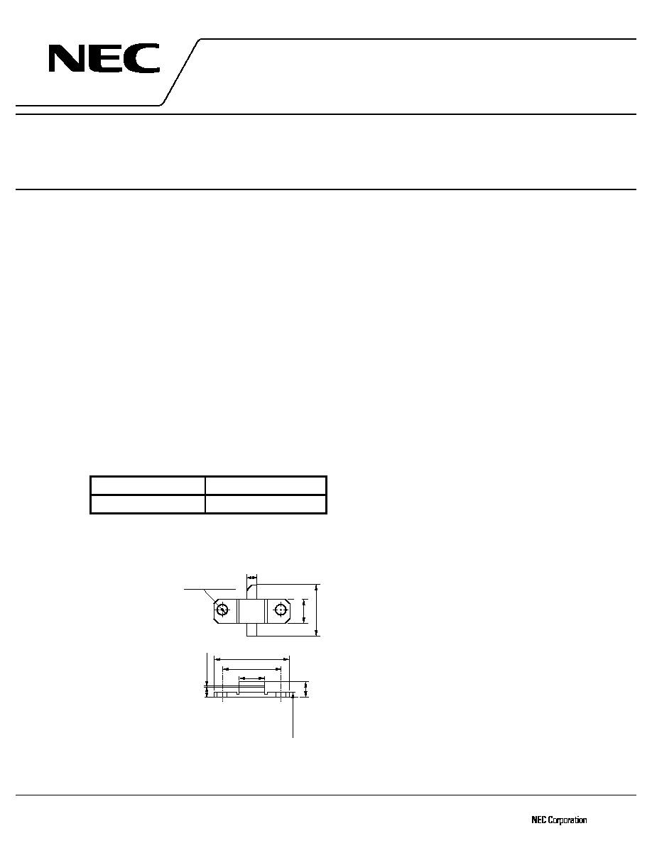
ORDERING INFORMATION
Part Number Package Outline
NEL2012F03-24 F03
PACKAGE DIMENSIONS PIN CONNECTIONS
(Unit: mm) 1. EMITTER
2. BASE
3. COLLECTOR
2
◊
3.3 ± 0.3
2.8 ± 0.2
6.35 ± 0.4
14.35 ± 0.4
18.9 ± 0.3
14.2 ± 0.3
6.35 ± 0.4
1.53 ± 0.3
2.17 ± 0.3
0.1
+0.05
4.67 ± 0.4
≠0.02
1
2
3

2
NEL2012F03-24
ABSOLUTE MAXIMUM RATINGS (T
A
= 25 ∞C)
PARAMETERS
SYMBOL
Specified Condition
RATINGS
UNIT
Collector to Base Voltage
V
CBO
45
V
Collector to Emitter Voltage
V
CER
R = 10
:
30
V
Emitter to Base Voltage
V
EBO
3
V
Collector to Emitter Voltage
V
CEO
18
V
Collector Current
I
C
4
A
Total Power Dissipation
P
T
41.5
W
Thermal Resistance
R
th (j-c)
4.2
∞C/W
Junction Temperature
T
j
200
∞C
Storage Temperature
T
stg
65 to +150
∞C
ELECTRICAL CHARACTERISTICS (T
A
= 25 ∞C)
PARAMETERS
SYMBOL
Specified Condition
MIN.
TYP.
MAX.
UNIT
Collector to Emitter Cutoff Current
I
CES
V
CE
= 24 V
8
mA
Collector to Emitter Voltage
V
CER
I
C
= 8 mA, R = 10
:
30
85
V
Collector to Emitter Voltage
V
CEO
I
C
= 8 mA
18
22
V
Collector to Base Voltage
V
CEO
I
C
= 8 mA
45
85
V
Emitter to Base Voltage
V
EBO
I
C
= 20 mA
3
4.4
V
DC Current Gain
h
FE
V
CE
= 5 V, I
C
= 0.8 A
30
100
150
Output Capacitance
Cob
V
CE
= 24 V, freq = 1 MHz
12.6
pF
PERFORMANCE SPECIFICATIONS (T
A
= 25 ∞C)
CLASS AB OPERATION (Unless otherwise specified, freq = 1.97 GHz, V
CC
= 24 V, Iq = 75 mA)
PARAMETERS
SYMBOL
Specified Condition
MIN.
TYP.
MAX.
UNIT
Output Power
P
1dB
12
16
W
Collector Efficiency
K
C
Pout = P
1dB
40
55
%
Linear Gain
G
L
Pin = 0.5 W
10.9
dB
3rd Order Intermodulation
IM
3
'
freq = 100 kHz, 12 W PEP
33
dBc
CLASS A OPERATION (Unless otherwise specified, freq = 1.97 GHz, V
CC
= 20 V, Iq = 750 mA)
PARAMETERS
SYMBOL
Specified Condition
MIN.
TYP.
MAX.
UNIT
Output Power
P
1dB
5
W
Collector Efficiency
K
C
Pout = P
1dB
35
%
Linear Gain
G
L
Pin = 0.07 W
13.8
dB
3rd Order Intermodulation
IM
3
'
freq = 100 kHz, 2.5 W PEP
35
dBc

3
NEL2012F03-24
NEL2012F03-24
Typical Pout-Gain, Collector Efficiency (N
C
) and Collector Current (I
C
) Characteristics
Gain
[dB]
18
17
16
15
14
13
12
11
10
9
8
7
6
5
4
3
28
30
32
34
36
38
40
42
Pout [dBm]
Nc
[%]
Ic
[A]
3
2.8
2.6
2.4
2.2
2
1.8
1.6
1.4
1.2
1
.8
.6
.4
.2
0
100
90
80
70
60
50
40
30
20
10
0
freq = 1.970 GHz
U
CC
= 24.0 V
Icq = 0.075 A
freq = 1.970 GHz
U
CC
= 20.0 V
Icq = 0.750 A
Class AB
Gain
[dB]
18
17
16
15
14
13
12
11
10
9
8
7
6
5
4
3
24
26
28
30
32
34
36
38
Pout [dBm]
Nc
[%]
Ic
[A]
3
2.8
2.6
2.4
2.2
2.0
1.8
1.6
1.4
1.2
1
.8
.6
.4
.2
0
100
90
80
70
60
50
40
30
20
10
0
Class A
Gain
Ic
Nc
Gain
Nc
Ic

4
NEL2012F03-24
NEL2012F03-24
Typical Pout (PEP) - Intermodulation (IM) Characteristics
≠20
≠30
≠40
≠50
≠60
20
30
40
P
OUT
(PEP)[dBm]
IM
[dBc]
Class AB (f = 1.97 GHz, V
CC
= 24 V, Icq = 0.075A)
IM3
IM5
IM7
≠20
≠30
≠40
≠50
≠60
20
30
40
P
OUT
(PEP)[dBm]
IM
[dBc]
Class A (f = 1.97 GHz, V
CC
= 20 V, Icq = 0.75A)
IM3
IM5
IM7

5
NEL2012F03-24
45
44.5
44
43.5
43
42.5
42
41.5
41
40.5
40
P
1dB
[dBm]
G
L
[dB]
1.9
1.92
1.94
1.96
1.98
2
2
3
4
5
6
7
8
9
10
P
1dB
G
L
11
12
Freq [GHz]
NEL2012F03-24 Frequency Characteristics
V
CC
= 24 v Icq = 0.075 A (Class AB)

6
NEL2012F03-24
NEL2012F03-24 Zin/Zout
2.0
5.0
0
0.1
0.2
0.3
0.4
0.5
0.6
0.7
0.8
0.9
1.0
1.2
1.4
1.6
1.8
2.0
3.0
4.0
10
50
20
50
10
6.0
4.0
3.0
1.8
1.6
1.4
0.2
1.0
0.9
0.8
0.7
0.6
0.5
0.4
0.3
0.2
0.1
20
(
+JX
≠≠≠≠
Z
O
)
0.2
1.0
0.8
0.6
0.4
0.2
0.4
0.6
0.8
1.0
2.0
50
10
6.0
4.0
3.0
1.8
1.6
1.4
1.2
1.0
0.9
0.8
0.7
0.6
0.3
0.2
0.1
20
1.0
0.8
0.6
0.4
0.2
0.4
0.6
0.8
1.0
0.4
0.5
NE
GA
TIV
E
RE
A
CT
A
N
C
E C
OM
P
O
N
E
N
T
(
≠ JX
≠≠≠≠
Z
O
)
P
OS
IT
IV
E
R
E
A
C
TA
N
C
E
CO
M
PO
NE
NT
(
R
≠≠≠≠
Z
O
)
1 : 1.8 GHz
2 : 1.9
3 : 1.97
4 : 2.0
REACTANCE COMPONENT
1
1
Z
IN
Z
OUT
2
2
3
3
4
4
Z0 = 50
:
f [GHz]
1.80
1.90
1.97
2.00
Zin [
:
]
4.3 + j8.9
3.1 + j7.4
2.6 + j6.3
2.4 + j5.9
Zout [
:
]
2.6 + j2.2
2.4 + j1.3
2.2 + j0.6
2.2 + j0.4
Zout
Zin

7
NEL2012F03-24
NEL2012F03-24 Class A S-Parameters
V
CC
= 20 V, Icq = 0.75 A
Freq
S
11
S
21
S
12
S
22
(GHz)
MAG
ANG
MAG
ANG
MAG
ANG
MAG
ANG
1.70
0.846
167.1
1.063
47.2
0.034
53.2
0.793
178.0
1.71
0.844
167.1
1.074
46.1
0.034
53.2
0.798
178.2
1.72
0.842
167.2
1.077
44.5
0.033
51.2
0.803
177.7
1.73
0.841
167.4
1.080
43.3
0.032
50.7
0.809
177.8
1.74
0.840
167.5
1.080
42.2
0.033
49.2
0.812
177.7
1.75
0.839
167.6
1.081
41.1
0.032
48.0
0.814
178.0
1.76
0.837
167.7
1.089
40.1
0.031
47.7
0.822
177.7
1.77
0.837
167.9
1.095
38.3
0.030
46.4
0.830
177.5
1.78
0.836
168.0
1.098
36.7
0.030
46.5
0.832
177.6
1.79
0.835
168.2
1.094
35.3
0.029
46.4
0.838
177.9
1.80
0.834
168.4
1.083
34.1
0.029
45.7
0.849
178.2
1.81
0.835
168.5
1.077
32.7
0.028
45.2
0.850
178.0
1.82
0.834
168.8
1.080
31.5
0.028
43.9
0.855
178.1
1.83
0.833
168.9
1.078
30.3
0.028
42.2
0.860
178.4
1.84
0.833
169.1
1.070
28.8
0.027
42.3
0.872
178.5
1.85
0.835
169.3
1.059
27.4
0.026
41.7
0.872
178.9
1.86
0.833
169.4
1.047
26.7
0.025
41.5
0.880
178.9
1.87
0.833
169.6
1.044
25.9
0.025
38.6
0.889
178.9
1.88
0.835
169.9
1.054
25.1
0.024
36.1
0.893
179.1
1.89
0.836
170.0
1.063
23.9
0.023
36.4
0.897
179.5
1.90
0.837
170.2
1.063
22.3
0.021
35.1
0.906
179.9
1.91
0.839
170.4
1.059
20.2
0.021
33.8
0.910
180.0
1.92
0.842
170.5
1.052
18.6
0.019
33.6
0.915
179.9
1.93
0.845
170.6
1.048
17.4
0.019
31.6
0.918
179.3
1.94
0.846
170.7
1.042
15.7
0.017
31.3
0.924
179.2
1.95
0.848
171.0
1.036
14.1
0.016
30.4
0.930
179.0
1.96
0.851
171.1
1.032
12.1
0.015
31.2
0.936
178.4
1.97
0.854
171.1
1.014
9.9
0.014
31.6
0.942
178.2
1.98
0.857
171.2
0.992
8.5
0.013
30.9
0.943
177.6
1.99
0.860
171.4
0.969
7.6
0.012
30.6
0.951
177.3
2.00
0.863
171.5
0.962
6.7
0.011
29.6
0.954
177.1

8
NEL2012F03-24
NEL2012F03-24 Class AB S-Parameters
V
CC
= 24 V, Icq = 0.075 A
Freq
S
11
S
21
S
12
S
22
(GHz)
MAG
ANG
MAG
ANG
MAG
ANG
MAG
ANG
1.70
0.916
166.1
0.366
28.1
0.019
63.0
0.938
175.4
1.71
0.915
166.0
0.371
27.5
0.019
63.5
0.940
175.8
1.72
0.912
165.9
0.375
26.1
0.019
63.0
0.942
175.9
1.73
0.911
165.9
0.376
24.9
0.018
62.4
0.943
176.1
1.74
0.910
165.8
0.378
24.3
0.018
62.0
0.944
176.3
1.75
0.909
165.8
0.378
23.7
0.018
61.1
0.944
176.6
1.76
0.906
165.6
0.381
23.2
0.017
61.4
0.946
176.8
1.77
0.905
165.5
0.382
21.8
0.017
62.3
0.950
177.0
1.78
0.903
165.5
0.387
20.4
0.017
61.6
0.949
177.2
1.79
0.901
165.4
0.386
19.4
0.017
63.3
0.951
177.5
1.80
0.899
165.4
0.384
18.4
0.017
61.5
0.954
177.8
1.81
0.897
165.3
0.382
17.4
0.017
61.0
0.954
177.9
1.82
0.896
165.3
0.385
16.4
0.017
59.6
0.958
178.1
1.83
0.893
165.3
0.387
15.8
0.017
60.4
0.957
178.5
1.84
0.890
165.2
0.383
14.3
0.016
60.0
0.962
178.6
1.85
0.890
165.3
0.383
13.3
0.016
60.0
0.962
178.9
1.86
0.886
165.2
0.383
12.5
0.015
58.4
0.963
178.9
1.87
0.883
165.2
0.385
12.5
0.016
56.7
0.964
179.2
1.88
0.882
165.3
0.388
11.9
0.015
55.9
0.968
179.5
1.89
0.879
165.3
0.396
10.6
0.014
55.3
0.967
179.6
1.90
0.877
165.4
0.402
9.5
0.014
53.6
0.967
180.0
1.91
0.876
165.4
0.403
7.3
0.013
55.3
0.968
179.8
1.92
0.874
165.5
0.403
6.0
0.013
53.7
0.968
179.6
1.93
0.873
165.4
0.405
4.6
0.012
54.0
0.968
179.2
1.94
0.871
165.5
0.402
3.2
0.012
51.1
0.969
179.1
1.95
0.869
165.6
0.408
1.7
0.011
52.4
0.969
178.9
1.96
0.867
165.7
0.407
0.8
0.011
49.9
0.970
178.6
1.97
0.867
165.8
0.405
2.8
0.009
51.3
0.971
178.3
1.98
0.865
165.9
0.401
4.3
0.009
51.8
0.971
178.0
1.99
0.864
166.0
0.396
5.2
0.008
50.6
0.971
177.7
2.00
0.863
166.2
0.393
6.3
0.007
50.6
0.972
177.5

9
NEL2012F03-24
Circuit Drawing
40 mm
40 mm
Through
Hole
1 mm
◊
4
1
1
1
1
1
1
1
1
2
1
1
0.5
0.5
5
5
5
8
8
3
6.6
6
22
22
15
15
2
11
50 mm
2.3
2.3
8.9
7.6
12.6
2
1
1
3.3
2
9.5
1
1 2
6
18.2
18.2
7.4
1
Input
Output
8
4.2
1
SUBSTRATE (TEFLON)
DICLAD522T
Æ
THICKNESS = 0.79 mm
DOUBLE SIDE 35
P
m Cu
H
r
= 2. 6
NEL2012F03-24

10
NEL2012F03-24
Components Layout
V
CC
V
BB
C4
C4
C3
D1
C2
C1
L1
R2
R1
R3
Input
Output
This lead is placed
near device flange.
R1: 5.1
:
R2: 50
:
R3: 47
:
L1: 5 mm
I
10T Coil
C1, C2, C3, C5: MURATA, 47 pF
C4: 100
P
F (50 V)
Electrolytic Capacitor
D1: V06C
NEL2012F03-24

11
NEL2012F03-24
[MEMO]

NEL2012F03-24
No part of this document may be copied or reproduced in any form or by any means without the prior written
consent of NEC Corporation. NEC Corporation assumes no responsibility for any errors which may appear in this
document.
NEC Corporation does not assume any liability for infringement of patents, copyrights or other intellectual
property rights of third parties by or arising from use of a device described herein or any other liability arising
from use of such device. No license, either express, implied or otherwise, is granted under any patents,
copyrights or other intellectual property rights of NEC Corporation or others.
While NEC Corporation has been making continuous effort to enhance the reliability of its semiconductor devices,
the possibility of defects cannot be eliminated entirely. To minimize risks of damage or injury to persons or
property arising from a defect in an NEC semiconductor device, customers must incorporate sufficient safety
measures in its design, such as redundancy, fire-containment, and anti-failure features.
NEC devices are classified into the following three quality grades:
"Standard", "Special", and "Specific". The Specific quality grade applies only to devices developed based on
a customer designated "quality assurance program" for a specific application. The recommended applications
of a device depend on its quality grade, as indicated below. Customers must check the quality grade of each
device before using it in a particular application.
Standard: Computers, office equipment, communications equipment, test and measurement equipment,
audio and visual equipment, home electronic appliances, machine tools, personal electronic
equipment and industrial robots
Special: Transportation equipment (automobiles, trains, ships, etc.), traffic control systems, anti-disaster
systems, anti-crime systems, safety equipment and medical equipment (not specifically designed
for life support)
Specific: Aircrafts, aerospace equipment, submersible repeaters, nuclear reactor control systems, life
support systems or medical equipment for life support, etc.
The quality grade of NEC devices is "Standard" unless otherwise specified in NEC's Data Sheets or Data Books.
If customers intend to use NEC devices for applications other than those specified for Standard quality grade,
they should contact an NEC sales representative in advance.
Anti-radioactive design is not implemented in this product.
M4 96. 5