
NESG2046M33
NEC's NPN SiGe TRANSISTOR
FOR LOW NOISE, HIGH -GAIN AMPLIFICATION
California Eastern Laboratories
∑
IDEAL FOR LOW NOISE, HIGH-GAIN AMPLIFICATION APPLICATIONS:
NF = 0.8 dB TYP., G
a
= 11.5 dB TYP. @ V
CE
= 1 V, I
C
= 3 mA, f = 2 GHz
∑
HIGH BREAKDOWN VOLTAGE TECHNOLOGY
FOR SIGE TRANSISTORS :
V
CEO
(absolute maximum ratings) = 5.0 V
∑ 3-PIN SUPER LEAD-LESS MINIMOLD (M33) PACKAGE
FEATURES
PRELIMINARY DATA SHEET
ORDERING INFORMATION
Remark To order evaluation samples, contact your nearby sales offi ce.
The unit sample quantity is 50 pcs.
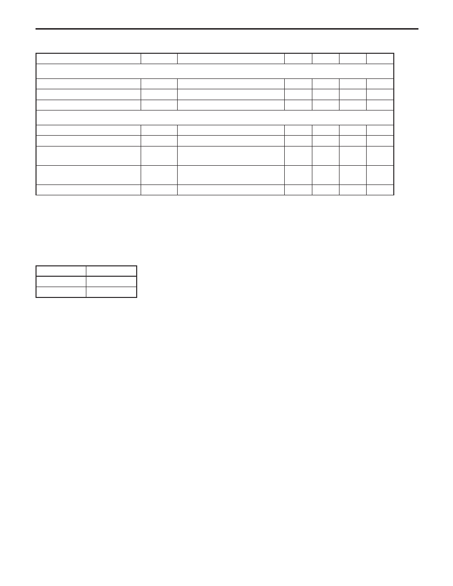
ABSOLUTE MAXIMUM RATINGS
(T
A
=+25∫C)
PARAMETER
SYMBOL
RATINGS
UNIT
Collector to Base Voltage
V
CBO
13
V
Collector to Emitter Voltage
V
CEO
5
V
Emitter to Base Voltage
V
EBO
1.5
V
Collector Current
I
C
40
mA
Total Power Dissipation
P
tot
Note
130
mW
Junction Temperature
T
j
150
∞
C
Storage Temperature
T
stg
-
65 to +150
∞
C
Note Mounted on 1.08 cm
2
◊
1.0 mm (t) glass epoxy PCB
Caution Observe precautions when handling because these devices are sensitive to electrostatic discharge.
PART NUMBER
QUANTITY
SUPPLYING FORM
NESG2046M33-A
50 pcs (Non reel)
∑ 8 mm wide embossed taping
∑ Pin 2 (Base) face the perforation side of the tape
NESG2046M33-T3-A
10 kpcs/reel
NESG2046M33
ELECTRICAL CHARACTERISTICS
(T
A
=+25∫C)
Notes 1. Pulse measurement: PW
350
s, Duty Cycle
2%
2. Collector to base capacitance when the emitter grounded
h
FE
CLASSIFICATION
RANK
FB
Marking
T7
h
FE
Value
140 to 220
PARAMETER
SYMBOL
TEST CONDITIONS
MIN.
TYP.
MAX.
UNIT
DC Characteristics
Collector Cut-off Current
I
CBO
V
CB
= 5 V, I
E
= 0 mA
-
-
100
nA
Emitter Cut-off Current
I
EBO
V
EB
= 0.5 V, I
C
= 0 mA
-
-
100
nA
DC Current Gain
h
FE
Note 1
V
CE
= 1 V, I
C
= 2 mA
140
180
220
-
RF Characteristics
Gain Bandwidth Product
f
T
V
CE
= 1 V, I
C
= 15 mA, f = 2 GHz
15
18
-
GHz
Insertion Power Gain
|S
21e
|
2
V
CE
= 1 V, I
C
= 15 mA, f = 2 GHz
11
13
-
dB
Noise Figure
NF
V
CE
= 1 V, I
C
= 3 mA, f = 2 GHz,
Z
S
= Z
Sopt
, Z
L
= Z
Lopt
-
0.8
1.5
dB
Associated Gain
G
a
V
CE
= 1 V, I
C
= 3 mA, f = 2 GHz,
Z
S
= Z
Sopt
, Z
L
= Z
Lopt
9.5
11.5
-
dB
Reverse Transfer Capacitance
C
re
Note 2
V
CB
= 1 V, I
E
= 0 mA, f = 1 MHz
-
0.2
0.4
pF

NESG2046M33
PACKAGE DIMENSIONS
3-PIN SUPER LEAD-LESS MINIMOLD (M33)
(UNIT: mm)
Life Support Applications
These NEC products are not intended for use in life support devices, appliances, or systems where the malfunction of these products can reasonably
be expected to result in personal injury. The customers of CEL using or selling these products for use in such applications do so at their own risk and
agree to fully indemnify CEL for all damages resulting from such improper use or sale.
A Business Partner of NEC Compound Semiconductor Devices, Ltd.
09/09/2004
0.15
0.57
0.285
0.125
0.44±0.05
1
2
3
(Bottom View)
0.15
0.84±0.05
0.125
0.15
0.64±0.05
0.1
1
0.4 MAX.
T7
PIN CONNECTIONS
1. Emitter
2. Base
3. Collector