
NESG260234
NEC's NPN SiGe RF TRANSISTOR
FOR MEDIUM OUTPUT POWER
AMPLIFICATION (1 W)
3-PIN POWER MINIMOLD (34 PACKAGE)
California Eastern Laboratories
∑
THIS PRODUCT IS SUITABLE FOR
MEDIUM OUTPUT POWER (1 W) AMPLIFICATION
P
O
= 30 dBm TYP. @ V
CE
= 6 V, P
in
= 15 dBm, f = 460 MHz
P
O
= 30 dBm TYP. @ V
CE
= 6 V, P
in
= 20 dBm, f = 900 MHz
∑ MAXIMUM STABLE GAIN:
MSG
= 23 dB TYP @ V
CE
= 6 V, I
C
= 100 mA, f = 460 MHz
∑
SiGe TECHNOLOGY:
UHS2-HV process
∑
ABSOLUTE MAXIMUM RATINGS:
V
CBO
= 25 V
∑
3-PIN POWER MINIMOLD (34 PACKAGE)
FEATURES
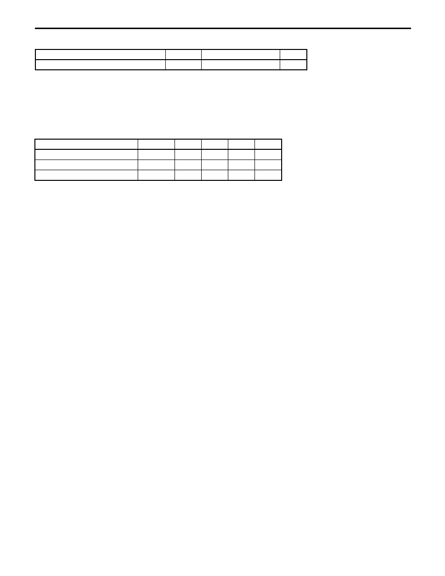
ORDERING INFORMATION
Remark To order evaluation samples, contact your nearby sales office.
Unit sample quantity is 25 pcs.
ABSOLUTE MAXIMUM RATINGS
(T
A
=+25∫C)
Note Mounted on 34.2 cm
2
◊ 0.8 mm (t) glass epoxy PWB
Caution Observe precautions when handling because these devices are sensitive to electrostatic discharge.
PART NUMBER
ORDER NUMBER
PACKAGE
QUANTITY
SUPPLYING FORM
NESG260234
NESG260234-AZ
3-pin power minimold
(Pb-Free)
Note1
25 pcs (Non reel) ∑ Magazine case
NESG260234-T1 NESG260234-T1-AZ
1 kpcs/reel
∑ 12 mm wide embossed taping
∑ Pin 2 (Emitter) face the perforation side of the tape
Notes 1. Contains Lead in the part except the electrode terminals.
PARAMETER
SYMBOL
RATINGS
UNIT
Collector to Base Voltage
V
CBO
25
V
Collector to Emitter Voltage
V
CEO
9.2
V
Emitter to Base Voltage
V
EBO
2.8
V
Collector Current
I
C
600
mA
Total Power Dissipation
P
tot
Note
1.9
W
Junction Temperature
T
j
150
∞
C
Storage Temperature
T
stg
-
65 to +150
∞
C
NESG260234
NESG260234
THERMAL RESISTANCE
(T
A
= 25∞C)
PARAMETER
SYMBOL
RATINGS
UNIT
Thermal Resistance from Junction to Ambient
Note
Rth
j-a
65
∞
C/W
Note Mounted on 34.2 cm
2
◊ 0.8 mm (t) glass epoxy PWB
RECOMMENDED OPERATING RANGE
(T
A
= 25∞C)
PARAMETER
SYMBOL
MIN.
TYP.
MAX.
UNIT
Collector to Emitter Voltage
V
CE
-
6.0
7.2
V
Collector Current
I
C
-
400
500
mA
Input Power
Note
P
in
-
15
20
dBm
Note Input power under conditions of V
CE
6.0 V, f = 460 MHz
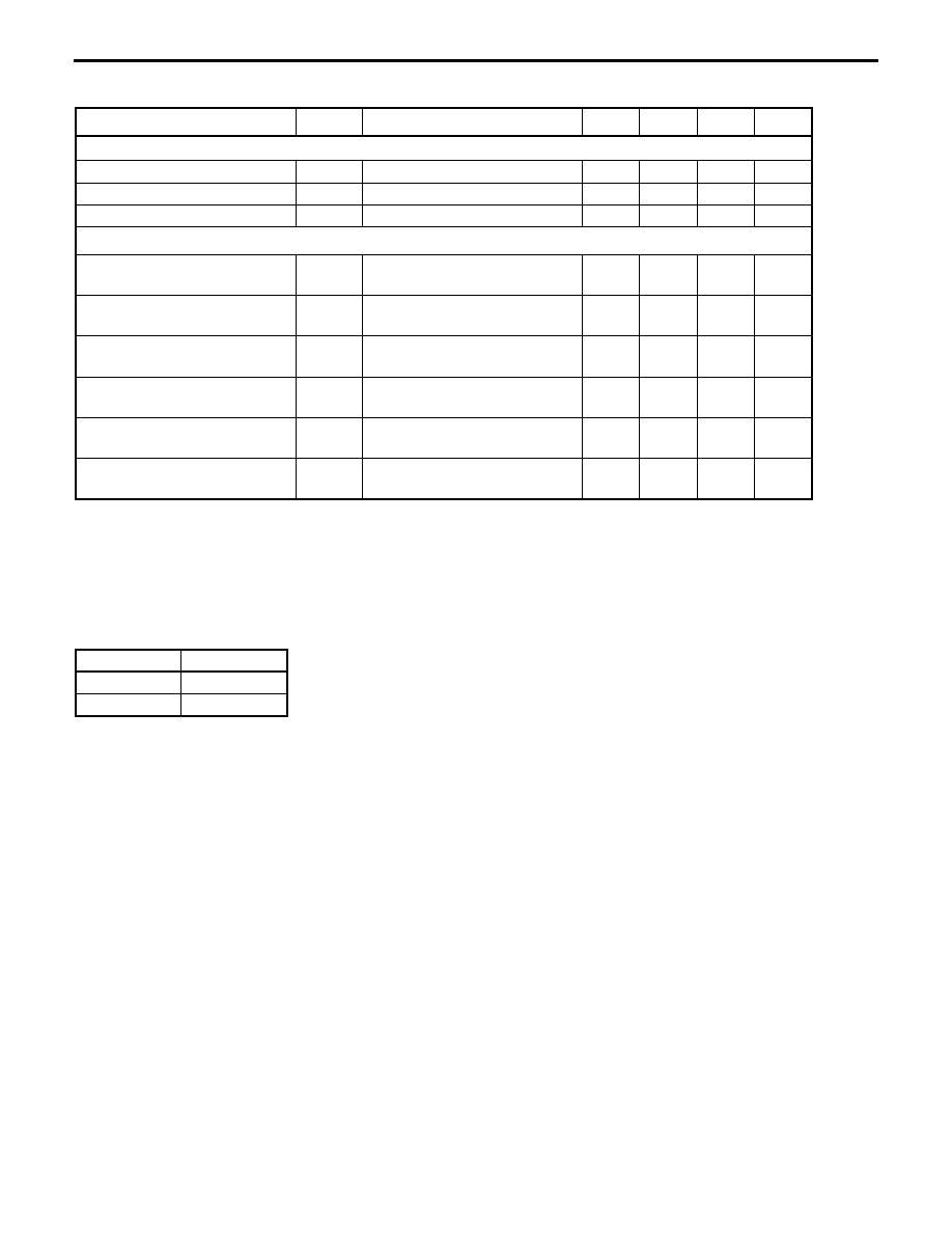
Notes 1. Pulse measurement: PW 350 s, Duty Cycle 2%
h
FE
CLASSIFICATION
NESG260234
NESG260234
ELECTRICAL CHARACHTERISTICS
(T
A
= 25∞C)
RANK
FB
Marking
SP
h
FE
Value
80 to 180
PARAMETER
SYMBOL
TEST CONDITIONS
MIN.
TYP.
MAX.
UNIT
DC Characteristics
Collector Cut-off Current
I
CBO
V
CB
= 9.2 V, I
E
= 0 mA
-
-
1
A
Emitter Cut-off Current
I
EBO
V
EB
= 1.0 V, I
C
= 0 mA
-
-
1
A
DC Current Gain
h
FE
Note
V
CE
= 3 V, I
C
= 100 mA
80
120
180
-
RF Characteristics
Linear gain (1)
G
L
V
CE
= 6 V, I
C (set)
= 30 mA (RF OFF),
f = 460 MHz, P
in
= 0 dBm
19
22
-
dB
Linear gain (2)
G
L
V
CE
= 6 V, I
C (set)
= 30 mA (RF OFF),
f = 900 MHz, P
in
= 0 dBm
-
19
-
dB
Output Power (1)
Po
V
CE
= 6 V, I
C (set)
= 30 mA (RF OFF),
f = 460 MHz, P
in
= 15 dBm
28.5
30.0
-
dBm
Output Power (2)
Po
V
CE
= 6 V, I
C (set)
= 30 mA (RF OFF),
f = 900 MHz, P
in
= 20 dBm
-
30.0
-
dBm
Collector Efficiency (1)
c
V
CE
= 6 V, I
C (set)
= 30 mA (RF OFF),
f = 460 MHz, P
in
= 15 dBm
-
50
-
%
Collector Efficiency (2)
c
V
CE
= 6 V, I
C (set)
= 30 mA (RF OFF),
f = 900 MHz, P
in
= 20 dBm
-
60
-
%

3-PIN POWER MINIMOLD (34 PACKAGE)
(UNIT:mm)
Life Support Applications
These NEC products are not intended for use in life support devices, appliances, or systems where the malfunction of these products can reasonably
be expected to result in personal injury. The customers of CEL using or selling these products for use in such applications do so at their own risk and
agree to fully indemnify CEL for all damages resulting from such improper use or sale.
A Business Partner of NEC Compound Semiconductor Devices, Ltd.
12/22/2004
PIN CONNECTIONS
1. Collector
2. Emitter
3. Base
1.5±0.1
0.41
+0.03
-0.06
4.5±0.1
0.42±0.06
0.42±0.06
1.6±0.2
3.0
1.5
2
1
3
2.5±0.1
4.0±0.25
0.8 MIN.
0.47±0.06
NESG260234