DATA SHEET
The information in this document is subject to change without notice. Before using this document, please
confirm that this is the latest version.
Not all devices/types available in every country. Please check with local NEC representative for
availability and additional information.
©
1997, 1999
Solid State Relay
OCMOS FET
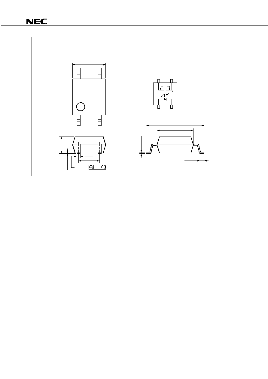
PS7200A-1A
4-PIN SOP 3.0 pF LOW OUTPUT CAPACITANCE
1-ch Optical Coupled MOS FET
Document No. P12636EJ4V0DS00 (4th edition)
Date Published October 1999 NS CP(K)
Printed in Japan
The mark
∑
∑
∑
∑
shows major revised points.
DESCRIPTION
The PS7200A-1A is a low output capacitance solid state relay containing GaAs LEDs on the light emitting side
(input side) and MOS FETs on the output side.
It is suitable for high-frequency signal control, due to its low C
◊
R, low output capacitance, and low off-state
leakage current.
FEATURES
∑ Low C
◊
R (C
◊
R = 30 pF ∑
)
∑ Low output capacitance (C
out
= 3.0 pF TYP.)
∑ Low off-state leakage current (I
Loff
= 0.1 nA TYP.)
∑ High-speed turn-on time (t
on
= 0.01 ms TYP.)
∑ 1 channel type (1 a output)
∑ Low LED operating current (I
F
= 2 mA)
∑ Designed for AC/DC switching line changer
∑ Small and thin package (4-pin SOP, Height = 2.1 mm)
∑ Low offset voltage
∑ Ordering number of taping product: PS7200A-1A-E3, E4, F3, F4
∑ UL approved: File No. E72422 (S)
∑ BSI approved: No. 8241/8242
∑ CSA approved: No. CA 101391
APPLICATIONS
∑ Measurement equipment
Data Sheet P12636EJ4V0DS00
3
PS7200A-1A
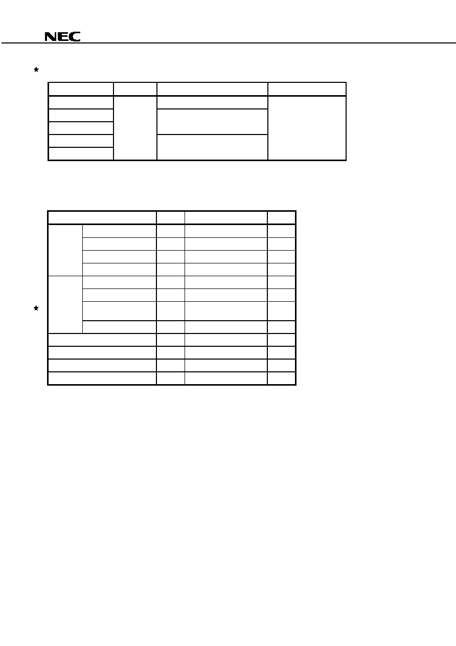
ORDERING INFORMATION
Part Number
Package
Packing Style
Application Part Number
*1
PS7200A-1A
4-pin SOP
Magazine case 100 pcs
PS7200A-1A
PS7200A-1A-E3
Embossed Tape 900 pcs/reel
PS7200A-1A-E4
PS7200A-1A-F3
Embossed Tape 3 500 pcs/reel
PS7200A-1A-F4
*1 For the application of the Safety Standard, following part number should be used.
ABSOLUTE MAXIMUM RATINGS (T
A
= 25
∞
∞
∞
∞
C, unless otherwise specified)
Parameter
Symbol
Ratings
Unit
Diode
Forward Current (DC)
I
F
50
mA
Reverse Voltage
V
R
5.0
V
Power Dissipation
P
D
50
mW
Peak Forward Current
*1
I
FP
1
A
MOS FET
Break Down Voltage
V
L
40
V
Continuous Load Current
I
L
100
mA
Pulse Load Current
*2
(AC/DC Connection)
I
LP
200
mA
Power Dissipation
P
D
100
mW
Isolation Voltage
*3
BV
1 500
Vr.m.s.
Total Power Dissipation
P
T
150
mW
Operating Ambient Temperature
T
A
-
40 to +80
∞
C
Storage Temperature
T
stg
-
40 to +100
∞
C
*1 PW = 100
µ
s, Duty Cycle = 1 %
*2 PW = 100 ms, 1 shot
*3 AC voltage for 1 minute at T
A
= 25
∞
C, RH = 60 % between input and output
Data Sheet P12636EJ4V0DS00
4
PS7200A-1A
RECOMMENDED OPERATING CONDITIONS (T
A
= 25
∞
∞
∞
∞
C)
Parameter
Symbol
MIN.
TYP.
MAX.
Unit
LED Operating Current
I
F
2
10
20
mA
LED Off Voltage
V
F
0
0.5
V
ELECTRICAL CHARACTERISTICS (T
A
= 25
∞
∞
∞
∞
C)
Parameter
Symbol
Conditions
MIN.
TYP.
MAX.
Unit
Diode
Forward Voltage
V
F
I
F
= 10 mA
1.2
1.4
V
Reverse Current
I
R
V
R
= 5 V
5.0
µ
A
MOS FET
Off-state Leakage Current
I
Loff
V
D
= 40 V
0.1
100
nA
Output Capacitance
C
out
V
D
= 0 V, f = 1 MHz
3.0
pF
Coupled
LED On-state Current
I
Fon
I
L
= 100 mA
2.0
mA
On-state Resistance
R
on1
I
F
= 10 mA, I
L
= 10 mA
9.3
12
R
on2
I
F
= 10 mA, I
L
= 100 mA, t
10 ms
Turn-on Time
*1
t
on
I
F
= 10 mA, V
O
= 5 V, PW
10 ms
0.01
0.5
ms
Turn-off Time
*1
t
off
0.07
0.2
Isolation Resistance
R
I-O
V
I-O
= 1.0 kV
DC
10
9
Isolation Capacitance
C
I-O
V = 0 V, f = 1 MHz
0.5
pF
*1 Test Circuit for Switching Time
V
L
R
L
I
F
R
in
Pulse Input
Input monitor
monitor
V
O
t
on
t
off
10 %
90 %
Input
0
Output
V
O
= 5 V
50 %

Data Sheet P12636EJ4V0DS00
5
PS7200A-1A
TYPICAL CHARACTERISTICS (T
A
= 25
∞
∞
∞
∞
C, unless otherwise specified)
≠25
0
25
50
75
80
100
100
80
60
40
0
20
Ambient Temperature T
A
(∞C)
Maximum Forward Current I
F
(mA)
MAXIMUM FORWARD CURRENT vs.
AMBIENT TEMPERATURE
1 mA
5 mA
20 mA
30 mA
I
F
= 50 mA
10 mA
≠25
0
25
50
75
100
1.6
1.4
1.2
1.0
0.8
Ambient Temperature T
A
(∞C)
Forward Voltage V
F
(V)
AMBIENT TEMPERATURE
FORWARD VOLTAGE vs.
f = 1 MHz
5
10
15
20
30
25
5.0
4.0
3.0
2.0
0
1.0
Applied Voltage V
D
(V)
Output Capacitance C
out
(pF)
OUTPUT CAPACITANCE vs.
APPLIED VOLTAGE
Ambient Temperature T
A
(∞C)
Maximum Load Current I
L
(mA)
MAXIMUM LOAD CURRENT vs.
AMBIENT TEMPERATURE
150
100
50
0
≠25
0
25
50
75
100
80
I
F
= 10 mA
≠2.0
≠1.0
1.0
2.0
0
100
50
≠50
≠100
LOAD CURRENT vs. LOAD VOLTAGE
Load Voltage V
L
(V)
Load Current I
L
(mA)
Applied Voltage V
D
(V)
Off-state Leakage Current I
Loff
(A)
OFF-STATE LEAKAGE CURRENT vs.
APPLIED VOLTAGE
25 ∞C
T
A
= 80 ∞C
0
10
20
30
40
50
10
≠6
10
≠7
10
≠8
10
≠9
10
≠10
10
≠11
10
≠12