©
1995
PRELIMINARY DATA SHEET
PACKAGE DRAWINGS
(Unit: mm)
SILICON TRANSISTOR
The
µ
PA812T has built-in 2 low-voltage transistors which are designed to
amplify low noise in the VHF band to the UHF band.
FEATURES
∑
Low Noise
NF = 1.4 dB TYP. @ f = 1 GHz, V
CE
= 3 V, I
C
= 7 mA
∑
High Gain
|S
21e
|
2
= 12 dB TYP. @ f = 1 GHz, V
CE
= 3 V, I
C
= 7 mA
∑
A Small Mini Mold Package Adopted
∑
Built-in 2 Transistors (2
◊
2SC4227)
ORDERING INFORMATION
PART NUMBER
QUANTITY
PACKING STYLE
µ
PA812T
Loose products
Embossed tape 8 mm wide. Pin 6 (Q1
(50 PCS)
Base), Pin 5 (Q1 Emitter), Pin 4 (Q2 Emitter)
face to perforation side of the tape.
µ
PA812T-T1
Taping products
(3 KPCS/Reel)
Remark
If you require an evaluation sample, please contact an NEC Sales
Representative. (Unit sample quantity is 50 pcs.)
ABSOLUTE MAXIMUM RATINGS (T
A
= 25
∞
C)
PARAMETER
SYMBOL
RATING
UNIT
Collector to Base Voltage
V
CBO
20
V
Collector to Emitter Voltage
V
CEO
10
V
Emitter to Base Voltage
V
EBO
1.5
V
Collector Current
I
C
65
mA
Total Power Dissipation
P
T
150 in 1 element
mW
200 in 2 elements
Note
Junction Temperature
T
j
150
∞ C
Storage Temperature
T
stg
≠65 to +150
∞ C
Note
110 mW must not be exceeded in 1 element.
µ
PA812T
HIGH-FREQUENCY LOW NOISE AMPLIFIER
NPN SILICON EPITAXIAL TRANSISTOR
(WITH BUILT-IN 2
◊◊
◊◊
◊
2SC4227) SMALL MINI MOLD
Document No. P11465EJ1V0DS00 (1st edition)
Date Published June 1996 P
Printed in Japan
The information in this document is subject to change without notice.
PIN CONFIGURATION (Top View)
PIN CONNECTIONS
1. Collector (Q1)
2. Base (Q2)
3. Collector (Q2)
4. Emitter (Q2)
5. Emitter (Q1)
6. Base (Q1)
6
5
4
1
2
3
Q
1
Q
2
2.1±0.1
1.25±0.1
1
2
3
6
5
4
0.2
≠0
+0.1
0.65
0.65
1.3
2.0±0.2
0.9±0.1
0.7
0 to 0.1
0.15
≠0
+0.1
X
Y
µ
PA812T
2
ELECTRICAL CHARACTERISTICS (T
A
= 25
∞
C)
PARAMETER
SYMBOL
CONDITION
MIN.
TYP.
MAX.
UNIT
Collector Cutoff Current
I
CBO
V
CB
= 10 V, I
E
= 0
0.8
µ
A
Emitter Cutoff Current
I
EBO
V
EB
= 1 V, I
C
= 0
0.8
µ
A
DC Current Gain
h
FE
V
CE
= 3 V, I
C
= 7 mA
Note 1
70
240
Gain Bandwidth Product
f
T
V
CE
= 3 V, I
C
= 7 mA, f = 1 GHz
4.5
7.0
GHz
Feed-back Capacitance
C
re
V
CB
= 3 V, I
E
= 0, f = 1 MHz
Note 2
0.9
pF
Insertion Power Gain
|S
21e
|
2
V
CE
= 3 V, I
C
= 7 mA, f = 1 GHz
10
12
dB
Noise Figure
NF
V
CE
= 3 V, I
C
= 7 mA, f = 1 GHz
1.4
2.7
dB
h
FE
Ratio
h
FE1
/h
FE2
V
CE
= 3 V, I
C
= 7 mA
0.85
A smaller value among
h
FE
of h
FE
1 = Q1, Q2
A larger value among
h
FE
of h
FE
2 = Q1, Q2
Notes 1. Pulse Measurement: Pw
350
µ
s, Duty cycle
2 %
2. Measured with 3-pin bridge, emitter and case should be connected to guard pin of bridge.
h
FE
CLASSIFICATION
Rank
FB
GB
Marking
34R
35R
h
FE
Value
70 to 150
110 to 240
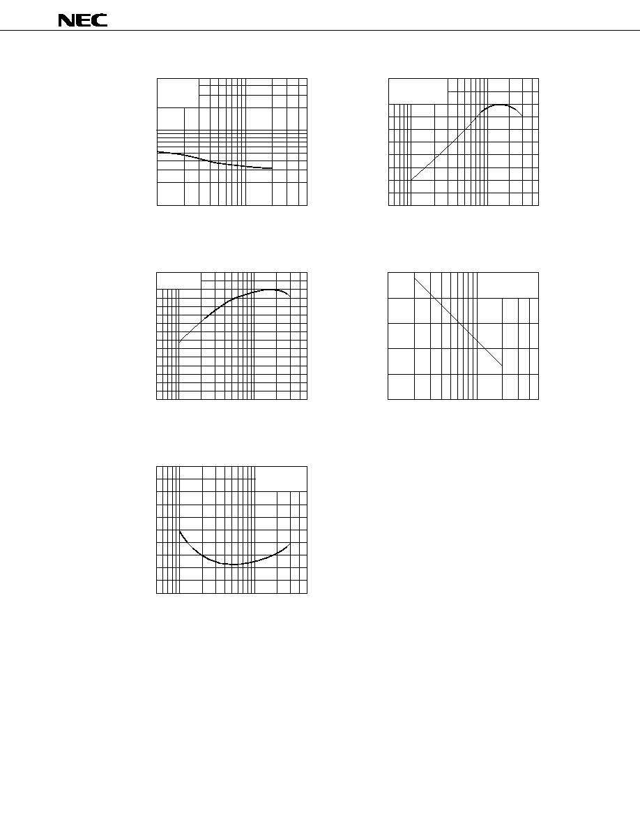
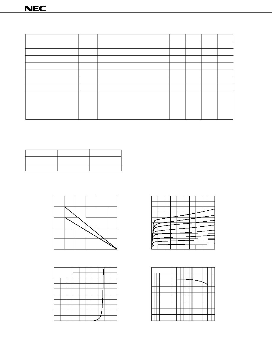
TYPICAL CHARACTERISTICS (T
A
= 25
∞
C)
5
0
10
0.5
0.5
1.0
10
15
20
0
0.5
1.0
10
20
1
5
10
50
20
50
100
200
V
CE
= 3 V
V
CE
= 3 V
25
P
T
- T
A
Characteristics
100
0
50
100
150
200
Total Power Dissipation P
T
(mW)
Ambient Temperature T
A
(∞C)
Free Air
2 Elements in Total
Per Element
Collector Current I
C
(mA)
Base to Emitter Voltage V
BE
(V)
I
C
- V
BE
Characteristics
Collector to Emitter Voltage V
CE
(V)
Collector Current I
C
(mA)
Collector Current I
C
(mA)
DC Current Gain h
FE
h
FE
- I
C
Characteristics
I
C
- V
CE
Characteristics
160 A
µ
140 A
µ
120 A
µ
100 A
µ
80 A
µ
60 A
µ
40 A
µ
I
B
= 20 A
µ