 | –≠–ª–µ–∫—Ç—Ä–æ–Ω–Ω—ã–π –∫–æ–º–ø–æ–Ω–µ–Ω—Ç: UPC1093J | –°–∫–∞—á–∞—Ç—å:  PDF PDF  ZIP ZIP |
©
1986
DATA SHEET
BIPOLAR ANALOG INTEGRATED CIRCUIT
µ
PC1093
ADJUSTABLE PRECISION SHUNT REGULATORS
Document No. G10634EJ5V0DS00 (5th edition)
(Previous No. IC-1791)
Date Published September 1998 N CP(K)
Printed in Japan
The mark shows major revised points.
The information in this document is subject to change without notice.
DESCRIPTION
The
µ
PC1093 are adjustable precision shunt regulators with guaranteed thermal stability. The output voltage can
be set to any value between reference voltage (2.495 V) and 36 V by two external resistors.
These ICs can apply to error amplifier of switching regulators.
FEATURES
∑
High Accuracy
V
REF
= 2.495 V
±
2 %
∑
Low Temperature Coefficient
V
REF
/
T
100 ppm/
∞
C
∑
Adjustable Output Voltage by two External Resistors
V
REF
V
O
36 V
∑
Low Dynamic Impedance
| Z
KA
| = 0.1
TYP.
ORDERING INFORMATION
Part Number
Package
µ
PC1093J
3-pin plastic SIP (TO-92)
µ
PC1093G
8-pin plastic SOP (225 mil)
µ
PC1093T
Power mini mold (SOT-89)
µ
PC1093TA
5-pin plastic mini mold (SC-74A)

µ
PC1093
2
EQUIVALENT CIRCUIT
PIN CONFIGURATION (Marking Side)
3-pin plastic SIP (TO-92)
8-pin plastic SOP (225 mil)
∑
µ
PC1093J
∑
µ
PC1093G
Power mini mold (SOT-89)
5-pin plastic mini mold (SC-74A)
∑
µ
PC1093T
∑
µ
PC1093TA
K
REF
A
R
5
R
6
R
7
R
8
R
9
R
10
R
1
R
2
R
3
R
4
Q
5
Q
6
Q
7
Q
8
Q
9
Q
10
Q
1
Q
2
Q
3
Q
4
Q
11
D
1
C
2
C
1
Q
12
Q
13
Q
14
Q
15
Q
16
Q
17
1
2
3
1 : REF
2 : A
3 : K
1
2
3
A
K
A REF
5
NC
4
A
1
3
2
REF A
K
REF : Reference
A : Anode
K : Cathode
NC : No Connection
1
2
3
4
8
7
6
5
K
NC
NC
NC
REF
NC
A
NC

µ
PC1093
3
ABSOLUTE MAXIMUM RATING (T
A
= 25
∞
C, unless otherwise specified.)
Parameter
Symbol
Ratings
Unit
Cathode Voltage
V
KA
37
V
Cathode Current
I
K
150
mA
Cathode-Anode Reverse Current
≠I
K
≠100
mA
Reference Voltage
V
REF
7
V
Reference Input Current
I
REF
50
µ
A
Reference-Anode Reverse Current
≠I
REF
≠10
mA
Power Dissipation
µ
PC1093J
P
T
700
mW
µ
PC1093G
480
µ
PC1093T
400/2 000
Note 1
µ
PC1093TA
180/510
Note 2
Operating Ambient Temperature
T
A
≠20 ~ +85
∞
C
Storage Temperature
T
stg
≠65 ~ +150
∞
C
Notes 1. with 16 cm
2
◊
0.7 mm ceramic substrate
2. with 75 mm
2
◊
0.7 mm ceramic substrate
Caution Exposure to Absolute Maximum Ratings for extended periods may affect device reliability; exceed-
ing the ratings could cause permanent damage. The parameters apply independently. The device
should be operated within the limits specified under DC and AC Characteristics.
RECOMMENDED OPERATING CONDITIONS
Parameter
Symbol
MIN.
TYP.
MAX.
Unit
Cathode Voltage
V
KA
V
REF
5
36
V
Cathode Current
I
K
1
10
100
mA
Power Dissipation
µ
PC1093J
P
T
50
220
mW
µ
PC1093G
50
150
µ
PC1093T
50
125/640
Note 1
µ
PC1093TA
50
58/160
Note 2
Operating Ambient Temperature
T
A
≠20
+85
∞
C
Notes 1. with 16 cm
2
◊
0.7 mm ceramic substrate
2. with 75 mm
2
◊
0.7 mm ceramic substrate

µ
PC1093
4
ELECTRICAL CHARACTERISTICS (T
A
= 25
∞
C, I
K
= 10 mA, unless otherwise specified.)
Parameter
Symbol
Conditions
MIN.
TYP.
MAX.
Unit
Reference Voltage
V
REF
V
KA
= V
REF
2.440
2.495
2.550
V
Reference Voltage Deviation Over
V
REF
0
∞
C
T
A
70
∞
C, V
KA
= V
REF
7
17
mV
Temperature
Reference Voltage Deviation Over
V
REF
/
V
| V
REF
|
V
KA
10 V
1.2
2.7
mV/V
Cathode Voltage
10 V
V
KA
36 V
0.7
2
mV/V
Reference Input Current
I
REF
V
KA
= V
REF
, R
1
= 10 k
, R
2
=
1
4
µ
A
Reference Input Current Deviation
I
REF
0
∞
C
T
A
70
∞
C, V
KA
= V
REF
,
0.4
1.2
µ
A
Over Temperature
R
1
= 10 k
, R
2
=
Minimum Cathode Current
I
K min.
V
KA
= V
REF
,
V
REF
= 2 %
0.4
1
mA
Off-state Cathode Current
I
K off
V
KA
= 36 V, V
REF
= 0
0.1
1
µ
A
Dynamic Impedance
| Z
KA
|
V
KA
= V
REF
, f
1 kHz
0.1
0.5
1 mA
I
K
100 mA
TEST AND APPLICATION CIRCUIT
V
IN
GND
K
A
REF
R
0
R
1
R
2
V
OUT
V
OUT
(1+ ) . V
REF
R
1
R
2
µ
PC1093
5
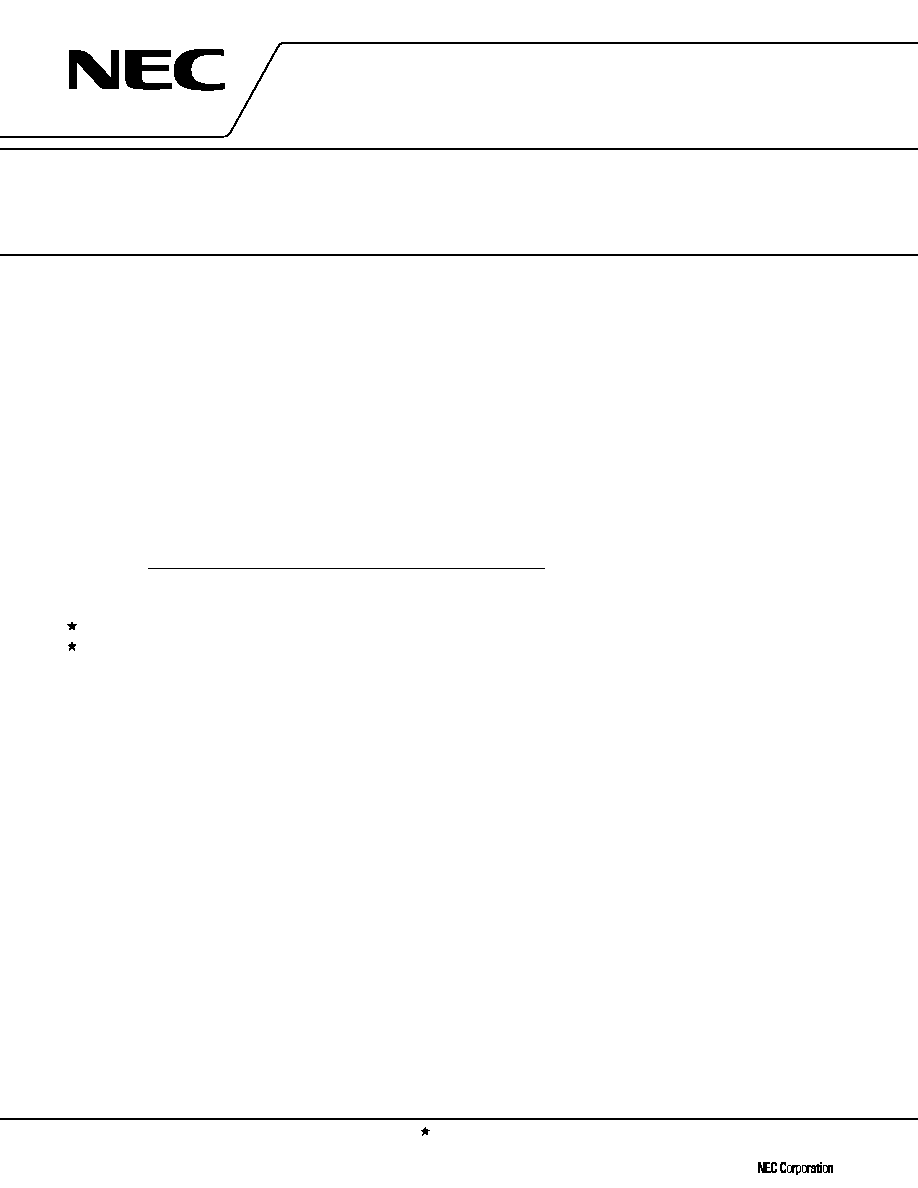
TYPICAL CHARACTERISTICS
1.2
0.2
1.0
0
2
1
3
V
KA
- Cathode Voltage - V
I
K
- Cathode Current - mA
I
K
vs
V
KA
(
I
)
0.8
0.4
0.6
T
A
= 25
∞
C
V
KA
= V
REF
20
10
0
≠10
≠20
0
≠25
50
75
100
T
A
- Operating Ambient Temperature -
∞
C
V
REF
- Reference Voltage Deviation - mV
V
REF
vs
T
A
20
10
≠20
40
V
KA
- Cathode Voltage - V
≠10
0
T
A
= 25
∞
C
I
K
= 10 mA
≠30
25
I
K
= 10 mA
V
KA
= V
REF
≠30
30
10
20
0
0.4
2.0
P
d
- Power Dissipation - W
P
d
vs
T
A
(
II
)
1.6
0.8
1.2
0.8
0.2
0.4
100
T
A
- Operating Ambient Temperature -
∞
C
P
d
- Power Dissipation - W
0.6
0
80
20
40
60
P
d
vs
T
A
(
I
)
(with 16 cm
2
◊
0.7 mm ceramic substrate)
PC1093T
PC1093J
PC1093TA
62.5
∞
C/W
180
∞
C/W
PC1093G
260
∞
C/W
PC1093T
315
∞
C/W
PC1093TA
695
∞
C/W
245
∞
C/W
150
100
50
0
≠50
≠2
≠1
0
1
2
3
V
KA
- Cathode Voltage - V
I
K
- Cathode Current - mA
I
K
vs
V
KA
(
II
)
T
A
= 25
∞
C
V
KA
= V
REF
≠100
µ
µ
µ
µ
100
0
80
20
40
60
T
A
- Operating Ambient Temperature -
∞
C
µ
µ
(with 75 mm
2
◊
0.7 mm ceramic
substrate)
V
REF
- Reference Voltage Deviation - mV
V
REF
vs
V
KA

µ
PC1093
6
0.3
0
25
50
75
100
T
A
-Operating Ambient Temperature -
∞
C
I
K off
- Off-state Cathode Current - A
I
K off
vs T
A
5
1
4
6
10
T - Time - s
V
REF
- Reference Voltage - V
Pulse Response
3
T
A
= 25
∞
C
V
KA
= V
REF
R
O
= 220
100
100 k
100
1 k
1 M
f - Frequency - Hz
Z
KAI
- Dynamic Impedance -
Z
KA
vs f
60
0
20
10 M
f - Frequency - Hz
A
v
- Voltage Gain - dB
A
v
vs f
40
0.01
10 k
T
A
= 25
∞
C
V
KA
= V
REF
1 mA
I
K
100 mA
≠20
1 M
10 k
100 k
1 k
0.1
0.2
0
≠25
V
KA
= 36 V
V
REF
= 0
0
0
2
0
2
8
220
I
K
o
in
10 k
(I
K
= 10 mA)
10 k
10
0.1
1
3
1
2
≠25
0
25
50
75
100
T
A
-Operating Ambient Temperature -
∞
C
I
REF
- Reference Input Current - A
I
REF
vs T
A
V
KA
= V
REF
, I
K
= 10 mA
R
1
= 10 k
, R
2
=
0
µ
µ
µ
~
V
IN
- Input Voltage - V

µ
PC1093
7
STABILITY AREA
TEST CIRCUIT
Caution of Stability Area
If the Aluminum electrolytic capacitor is used, it should be kept C
KA
2.2
µ
F.
When using plural different types of capacitors, each capacitor is needed to be stable independently.
When designing a circuit, take the characteristic variation among devices into consideration, so that the designed
circuit has an enough characteristic margin supporting the standard specifications described above.
100
90
80
70
60
50
40
30
20
10
0
I
KA
- Cathode Current - mA
C
KA
- Load Capacitance - F
0.001
0.01
0.1
1
10
a : V
KA
= V
REF
b : V
KA
= 5 V
c : V
KA
= 10 V
d : V
KA
= 15 V
Unstable
Stable
a
b
c
d
a
b
c
µ
Stable
I
KA
I
KA
150
150
C
KA
C
KA
10 k
R
a
b, c, d
C
KA
: Monolithic Ceramic Capacitors

µ
PC1093
8
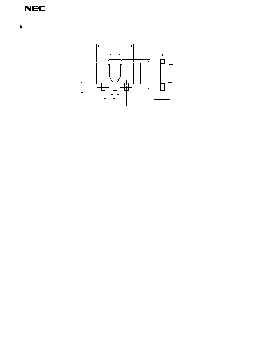
PACKAGE DRAWINGS
G
M
1
3
J
U
V
F
3 PIN PLASTIC SIP (TO-92)
A
M
Y
H
NOTE
Each lead centerline is located within 0.12 mm of
its true position (T.P.) at maximum material condition.
P3J-127B-2
ITEM
MILLIMETERS
A
F
G
H
J
M
N
U
5.0
±
0.2
0.12
5.0
±
0.5
4.0
±
0.2
0.5
V
Y
15.0
±
0.7
2.8 MAX.
0.5
±
0.1
1.27
1.33 MAX.
+
0.3
-
0.1
N

µ
PC1093
9
8 PIN PLASTIC SOP (225 mil)
M
C
D
F
8
5
1
4
M
G
E
B
P
J
K
L
N
S
detail of lead end
ITEM
MILLIMETERS
A
B
C
E
F
G
H
I
J
5.2
1.27 (T.P.)
1.59
±
0.21
1.49
6.5
±
0.3
0.78 MAX.
0.12
1.1
±
0.2
4.4
±
0.15
M
0.1
±
0.1
N
S8GM-50-225B-5
P
3
∞+
7
∞
D
0.42
+
0.08
-
0.07
K
0.17
+
0.08
-
0.07
L
0.6
±
0.2
0.10
-
3
∞
S
H
I
A
NOTE
Each lead centerline is located within 0.12 mm of
its true position (T.P.) at maximum material condition.
+
0.17
-
0.20
µ
PC1093
10
POWER MINI MOLD (SOT-89) (Unit: mm)
4.5
±
0.1
1.6
±
0.2
0.41
+
0.03
-
0.05
1.5
±
0.1
2.5
±
0.1
4.0
±
0.25
3.0
1.5
0.42
±
0.06
0.42
±
0.06
0.8 MIN.
0.47
±
0.06

µ
PC1093
11
5 PIN PLASTIC MINI MOLD
B
A
C
0.95 (T.P.)
2.9
±
0.2
0.3
S5TA-95-15A
ITEM
MILLIMETERS
B
R
K
M
L
detail of lead end
J
C
D
F
N
D
0.32
+
0.05
-
0.02
E
F
1.4 MAX.
0.05
±
0.05
G
1.1
+
0.2
-
0.1
H
2.8
±
0.2
I
1.5
+
0.2
-
0.1
J
0.65
+
0.1
-
0.15
K
0.16
+
0.1
-
0.06
M
N
R
5
∞±
5
∞
S
M
S
G
E
A
H
I
L
0.4
±
0.2
0.19
0.1
µ
PC1093
12
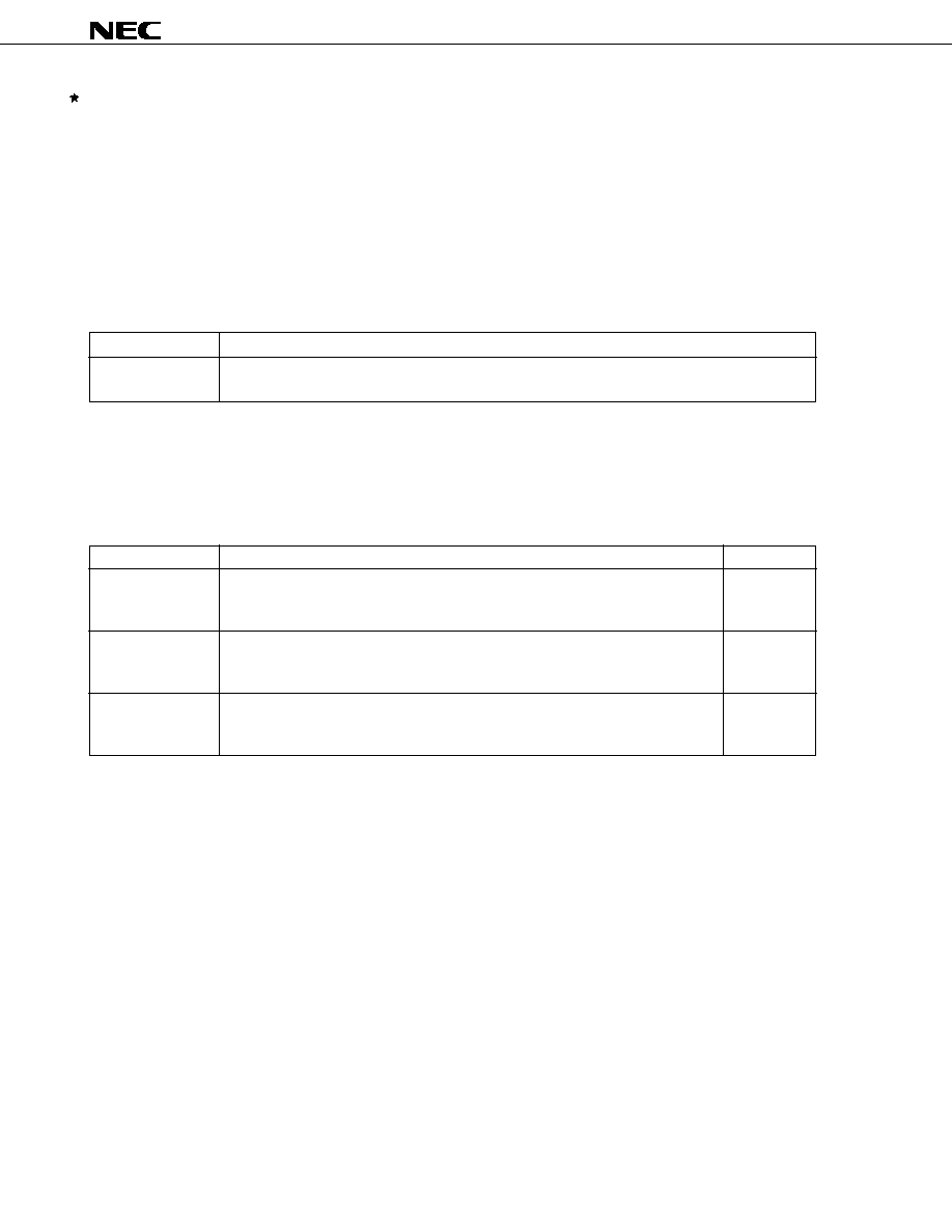
RECOMMENDED SOLDERING CONDITIONS
When soldering this product, it is highly recommended to observe the conditions as shown below. If other soldering
processes are used, or if the soldering is performed under different conditions, please make sure to consult with our
sales offices.
For more details, refer to our document "SEMICONDUCTOR DEVICE MOUNTING TECHNOLOGY MANUAL"
(C10535E).
Through-hole device
µ
PC1093J: 3-pin plastic SIP (TO-92)
Process
Conditions
Wave soldering
Solder temperature: 260
∞
C or below,
(only to leads)
Flow time: 10 seconds or less.
Caution For through-hole device, the wave soldering process must be applied only to leads, and make sure
that the package body does not get jet soldered.
Surface mount devices
µ
PC1093G: 8-pin plastic SOP (225 mil)
Process
Conditions
Symbol
Infrared ray reflow
Peak temperature: 230
∞
C or below (Package surface temperature),
IR30-00-1
Reflow time: 30 seconds or less (at 210
∞
C or higher),
Maximum number of reflow processes: 1 time.
VPS
Peak temperature: 215
∞
C or below (Package surface temperature),
VP15-00-1
Reflow time: 40 seconds or less (at 200
∞
C or higher),
Maximum number of reflow processes: 1 time.
Wave soldering
Solder temperature: 260
∞
C or below, Flow time: 10 seconds or less,
WS60-00-1
Maximum number of flow processes: 1 time,
Pre-heating temperature: 120
∞
C or below (Package surface temperature).
Caution Apply only one kind of soldering condition to a device, or the device will be damaged by heat stress.

µ
PC1093
13
µ
PC1093T: Power mini mold (SOT-89)
Process
Conditions
Symbol
Infrared ray reflow
Peak temperature: 235
∞
C or below (Package surface temperature),
IR35-00-2
Reflow time: 30 seconds or less (at 210
∞
C or higher),
Maximum number of reflow processes: 2 times.
VPS
Peak temperature: 215
∞
C or below (Package surface temperature),
VP15-00-2
Reflow time: 40 seconds or less (at 200
∞
C or higher),
Maximum number of reflow processes: 2 times.
Wave soldering
Solder temperature: 260
∞
C or below, Flow time: 10 seconds or less,
WS60-00-1
Maximum number of flow processes: 1 time,
Pre-heating temperature: 120
∞
C or below (Package surface temperature).
Caution Apply only one kind of soldering condition to a device, or the device will be damaged by heat stress.
µ
PC1093TA: 5-pin plastic mini mold (SC-74A)
Process
Conditions
Symbol
Infrared ray reflow
Peak temperature: 235
∞
C or below (Package surface temperature),
IR35-00-3
Reflow time: 30 seconds or less (at 210
∞
C or higher),
Maximum number of reflow processes: 3 times.
VPS
Peak temperature: 215
∞
C or below (Package surface temperature),
VP15-00-3
Reflow time: 40 seconds or less (at 200
∞
C or higher),
Maximum number of reflow processes: 3 times.
Wave soldering
Solder temperature: 260
∞
C or below, Flow time: 10 seconds or less,
WS60-00-1
Maximum number of flow processes: 1 time,
Pre-heating temperature: 120
∞
C or below (Package surface temperature).
Caution Apply only one kind of soldering condition to a device, or the device will be damaged by heat stress.
µ
PC1093
14
REFERENCE DOCUMENTS
Quality Grades on NEC Semiconductor Devices
C11531E
Semiconductor Device Mounting Technology Manual
C10535E
IC Package Manual
C10943X
Semiconductors Selection Guide
X10679E
NEC Semiconductor Device Reliability/Quality Control System
IEI-1212
-Three Terminal Regulator
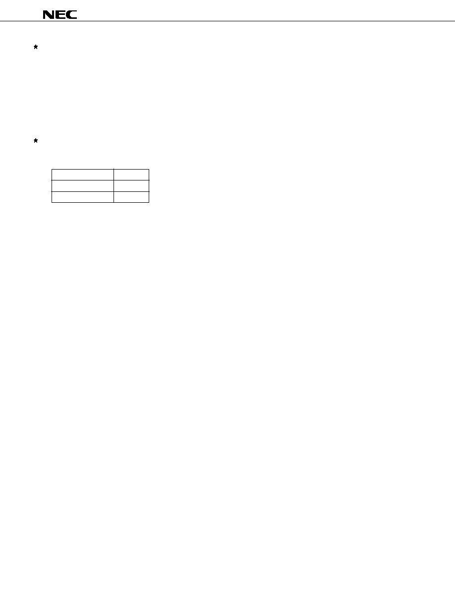
REMARK OF THE PACKAGE MARK
The package marks of the
µ
PC1093T and the
µ
PC1093TA are the symbols as follows.
Part Number
Mark
µ
PC1093T
93
µ
PC1093TA
K93

µ
PC1093
15
[MEMO]

µ
PC1093
No part of this document may be copied or reproduced in any form or by any means without the prior written
consent of NEC Corporation. NEC Corporation assumes no responsibility for any errors which may appear in
this document.
NEC Corporation does not assume any liability for infringement of patents, copyrights or other intellectual property
rights of third parties by or arising from use of a device described herein or any other liability arising from use
of such device. No license, either express, implied or otherwise, is granted under any patents, copyrights or other
intellectual property rights of NEC Corporation or others.
While NEC Corporation has been making continuous effort to enhance the reliability of its semiconductor devices,
the possibility of defects cannot be eliminated entirely. To minimize risks of damage or injury to persons or
property arising from a defect in an NEC semiconductor device, customers must incorporate sufficient safety
measures in its design, such as redundancy, fire-containment, and anti-failure features.
NEC devices are classified into the following three quality grades:
"Standard", "Special", and "Specific". The Specific quality grade applies only to devices developed based on a
customer designated "quality assurance program" for a specific application. The recommended applications of
a device depend on its quality grade, as indicated below. Customers must check the quality grade of each device
before using it in a particular application.
Standard: Computers, office equipment, communications equipment, test and measurement equipment,
audio and visual equipment, home electronic appliances, machine tools, personal electronic
equipment and industrial robots
Special:
Transportation equipment (automobiles, trains, ships, etc.), traffic control systems, anti-disaster
systems, anti-crime systems, safety equipment and medical equipment (not specifically designed
for life support)
Specific:
Aircrafts, aerospace equipment, submersible repeaters, nuclear reactor control systems, life
support systems or medical equipment for life support, etc.
The quality grade of NEC devices is "Standard" unless otherwise specified in NEC's Data Sheets or Data Books.
If customers intend to use NEC devices for applications other than those specified for Standard quality grade,
they should contact an NEC sales representative in advance.
Anti-radioactive design is not implemented in this product.
M4 96.5
The application circuits and their parameters are for reference only and are not intended for use in actual design-ins.
[MEMO]