NEC's SiGe
LOW NOISE AMPLIFIER FOR
GPS/MO BILE COMMUNICATIONS
FEATURES
∑ LOW
NOISE:
N
F
= 1.3 dB TYP.
∑ HIGH
GAIN:
G
P
= 18.5 dB TYP.
∑ LOW CURRENT CONSUMPTION:
I
CC
= 3.5 mA TYP. at V
CC
= 3.0 V
∑ BUILT-IN POWER SAVE FUNCTION:
∑ HIGH-DENSITY SURFACE MOUNTING:
6-pin lead less minimold package ( 1.5 x 1.3 x 0.55 mm)
UPC8211TK
∑ Low Noise amplifi er for GPS and mobile communications
∑ General purpose low noise amplifi er
APPLICATION
NEC's UPC8211TK is a silicon germanium (SiGe) monolithic
integrated circuit designed as low noise amplifi er for GPS and
as a general low nois amplifi er for mobile communications.
The package is 6-pin lead-less minimold (1.5 x 1.3 x 0.55 mm)
suitable for surface mount and optimized for very densely
populated compact designs.
This IC is manufactured using NEC's 60 GHz f
T
UHS2 (Ultra
High Speed Pro cess) silicon bipolar process. This process
can realize excellent low noise peformance and low power
consumption simultaneously.
NEC's stringent quality assurance and test procedures en sure
the highest reliability and per for mance.
DESCRIPTION
ELECTRICAL CHARACTERISTICS,
(Un less otherwise specifi ed, T
A
= +25∞C, V
CC
= 3.0 V, f
in
= 1575 MHz, V
PS
= 3.0 V)
PART NUMBER
UPC8211TK
PACKAGE
OUTLINE
S06
SYMBOLS
PARAMETERS
AND
CONDITIONS
UNITS
MIN
TYP
MAX
I
CC
Circuit Current (no input signal)
mA
≠
3.5
4.5
At power save mode (V
PS
< 0.8V)
A ≠
≠ 1
GP
Power
Gain
dB 15.5 18.5 21.5
NF Noise
Figure
dB
≠
1.3
1.5
IIP
3
3rd Order Distortion Input Intercept Point (Gain = 18.5 dB)
dBm
≠
-12
≠
RL
IN
Input Return Loss
dB
≠
-7.5
-6
RL
OUT
Output Return Loss
dB
≠
-14.5
-10
ISO Isolation
dBm
≠
-32.5
≠
V
PS ON
Rising Voltage from Power-Saving Mode
V
2.2
≠
≠
V
PS OFF
Falling Voltage from Power-Saving Mode
V
≠
≠
0.8
Flat
Gain Flatness (fi n ±2.5 MHz)
dB
≠
≠
0.5
P
o(1 dB)
Gain1 dB Compression Output Power
dBm
≠
-4
≠
P
o
Output Power
dBm
-1.5
+2.0
≠
California Eastern Laboratories
INTERNAL BLOCK DIAGRAM
1
2
3
6
4
5
GND
GND
Bias
Vcc
Input
Output
PS

TEST CIRCUITS
UPC8211TK
ABSOLUTE MAXIMUM RATINGS
1
(T
A
= 25∞C)
SYMBOLS
PARAMETERS
UNITS
RATINGS
V
CC
Supply Voltage
V
4.0
P
D
Power Dissipation
mW
232
T
A
Operating Ambient
∞C
-40 to +85
Temperature
T
STG
Storage Temperature
∞C
-55 to +150
P
IN
Input Power
dBm
+10
SYMBOLS PARAMETERS
UNITS
MIN
TYP
MAX
V
CC
Supply
Voltage
V 2.7 3.0 3.3
T
A
Operating Ambient
∞C
-25
+25
+85
Temperature
f
in
Operating
Frequency
MHz ≠ 1575 ≠
Range
RECOMMENDED
OPERATING CON DI TIONS
Notes:
1. Mounted on a double-sided copper-clad 50 x 50 x 1.6 mm epoxy
glass PWB
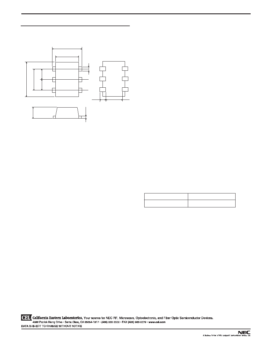
PIN CONNECTIONS
PIN NO.
PIN NAME
1 INPUT
2 GND
3 PS
4 OUTPUT
5 GND
6 V
CC
4
5
6
1
2
3
6G
(Top View)
(Bottom View)
750
0.1 µF
0.1 µF
8.2 nH
4.7 nH
22 nH
4
5
1
2
3
6
Hi: ON
Low: OFF (Power Save)
82 pF
33 pF
1.3 pF
OUT
IN
VPS
VCC