Document Outline
- COVER
- DESCRIPTION
- FEATURES
- ORDERING INFORMATION
- 1. BLOCK DIAGRAM/SYSTEM DIAGRAM
- 1.1 Boost Voltage Construction
- 1.2 Boost Voltage Auto Start and Rising Order
- 1.3 VS_AMP Circuit
- 1.4 Common Drive Circuit
- 1.5 Variable Boost Steps
- 2. PIN CONFIGURATION (Pad Layout)
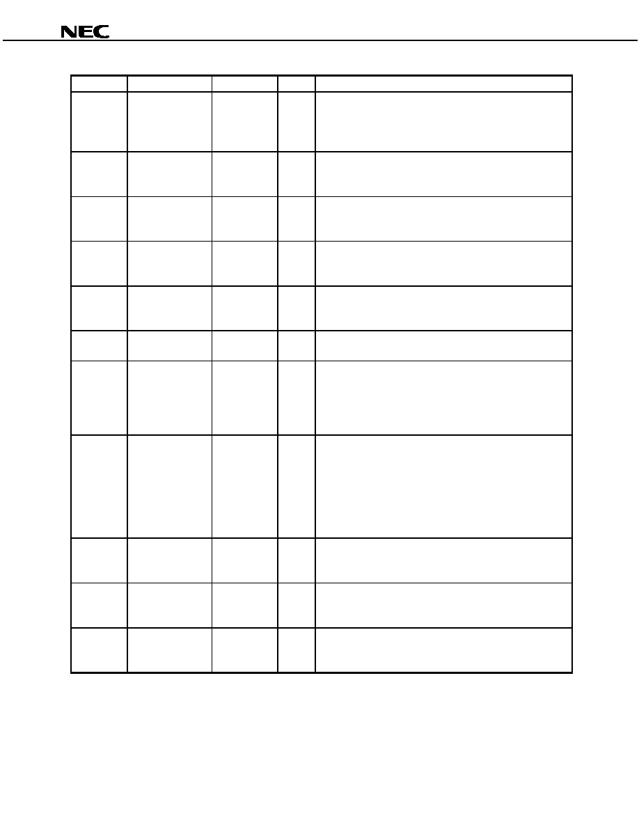
- 3. PIN FUNCTIONS
- 4. COMMAND
- 4.1 Command List
- 4.2 Command Description
- 4.3 Command Setting Values When IFSEL = H (When Using Control Pins)
- 5. MODE DESCRIPTION
- 5.1 Output Mode and Gate Scan Selection
- 5.2 DC/DC OSC Frequency Selection
- 5.3 DC/DC Converter Control
- 5.4 VDD2 Boost Selection
- 5.5 Division Ratio Selection of the DC/DC Converter at Power on
- 5.6 DC/DC Converter Power on Time Selection
- 5.7 Division Ratio Selection of the DC/DC Converter OSC Frequency
- 5.8 Amp. Current Selection
- 5.9 VR Regulator Selection Output
- 5.10 VS Regulator Selection Output
- 5.11 Control of VM Output Control, VCOM Output
- 5.12 VCOM Output Frequency Adjustment
- 5.13 VCOM Output Center Adjustment
- 5.14 VCOM Center Adjustment Selection
- 6. PANNEL CONNECTION
- 7. CONNECTION EXAMPLE WITH SOURCE DRIVER
- 8. VALUE OF WIRING RESISTANCE TO EACH PIN
- 9. RECOMMENDED CAPACITANCE VALUES OF EXTERNAL CAPACITOR
- 10. SERIAL INTERFACE
- 11. TIMING CHARTS (MODE1: SCN0 = 1, SCN1 = 1, SCN2 = 1)
- 12. POWER ON/OFF SEQUENCE
- 12.1 Power ON sequence
- 12.2 Power OFF sequence
- 13. ELECTRICAL SPECIFICATIONS
©
2001
MOS INTEGRATED CIRCUIT
µ
µ
µ
µ
PD161644
241 OUTPUT GATE DRIVER WITH POWER SUPPLY FOR TFT-LCD GATE DRIVER
PRELIMINARY PRODUCT INFORMATION
Document No. S15797EJ1V4PM00 (1st edition)
Date Published October 2002 NS CP(K)
Printed in Japan
The information contained in this document is being issued in advance of the production cycle for the
device. The parameters for the device may change before final production or NEC Corporation, at its own
discretion, may withdraw the device prior to its production.
Not all devices/types available in every country. Please check with local NEC representative for
availability and additional information.
The mark
!
shows major revised points.
DESCRIPTION
The
µ
PD161644 is a TFT-LCD gate driver with power supply for TFT-LCD driver. Because this gate driver has a
level shift circuit for logic input, it can output a high gate scanning voltage in response to a CMOS-level input. This
ICs can generate the levels which TFT-LCD driver need, from 2.7 V.
FEATURES
∑
High breakdown voltage output (V
DD1
-V
SS3
= 40 V MAX.)
∑
2.7 V CMOS level input
∑
Number of output: 241 output selectable
∑
To generate 4 levels from single voltage input
∑
To integrate regulator circuit for source driver
∑
Mode setting from source driver: Serial I/F or pin control
∑
On-chip VCOM driver
∑
On-chip gate output low-level selector
ORDERING INFORMATION
Part number
Package
µ
PD161644P
Chip
Remark
Purchasing the above chip entails the exchange of documents such as a separate memorandum or
product quality, so please contact one of our sales representatives.
Preliminary Product Information S15797EJ1V4PM
2
µ
µ
µ
µ
PD161644
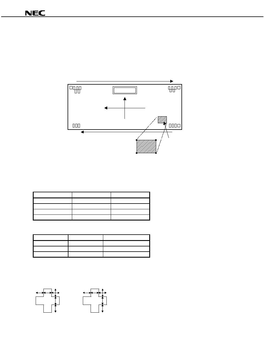
1. BLOCK DIAGRAM/SYSTEM DIAGRAM
SR121 SR122
SR240
SR241
SCN1
SR120
SR119
SR2
SR1
C2
V
DD2
V
DD1
V
SS2
GCS
GCL
V
SS1
IFSEL
MVS
C2
C5
+
C5
-
C2
C4
+
C4
-
C2
C3
+
C3
-
C1
C2
+
C2
-
C1
C1
+
C1
-
V
CC1
V
DC
V
S
5 V
4 V
V
REF
Regurator
V
S
GDA
DC/DC converter
R,/L
CLK
STVR
OE
1
OE
2
MPX
O
1
O
2
O
119
O
120
O
122
O
122
O
240
O
241
STVL
V
B
PV
SS3
PV
CC1
VCIN
VCOM
COMH
COML
V
SS3
DCON
RGONR
VM
VCD2
V
DC
SCN0
/GRESET
C2
C2
C2
C2
C6
+
C6
-
C2
V
SS4
C2
C2
V
DC
D/A
OSC
DCCLK
VSEL
EXRV
CLS0
FS0
FS2
PUPT0
DUPF0
DC/DC converter
DC/DC converter
Common
driver
circuit
Source driver
Serial interface
register
Switch
Level Shifter
Gate output
low level select circuit
ACS0
Source driver
Common
VMS
RGON
SCN2
FRM
VMON
TESTIN1
TESTIN2
TESTOUT1
TESTOUT2
D/A
Regurator
V
R
VGD
V
R
PV
SS1
VCOMIN
C2
C3
Remarks 1./xxx indicates active low signal.
2.Level Shifter (LS): Interfaces between 2.7 V CMOS level and V
DD1
to V
B
level.
Preliminary Product Information S15797EJ1V4PM
3
µ
µ
µ
µ
PD161644
1.1 Boost Voltage Construction
The boost voltage generated in
µ
PD161644 is shown below.
V
DD2
: 5.4 V
V
SS1
: 0 V
V
R
: 5 V
V
DD1
= V
R
x 3
= 15 V
V
DC
: 2.7 V
V
SS2
= V
R
x
-
2
=
-
10 V
V
SS3
= V
R
x
-
3
=
-
15 V
V
DD2
: 5.4 V
V
SS1
: 0 V
V
R
: 5 V
V
DD1
= V
DD2
x 3
= 16.2 V
V
DC
: 2.7 V
V
SS2
= V
DD2
x
-
2
=
-
10.8 V
V
SS3
= V
DD2
x
-
3
=
-
16.2 V
V
SS4
= V
DC
x
-
1
=
-
2.7 V
V
SS4
= V
DC
x
-
1
=
-
2.7 V
VGD = V
R
VGD = V
DD2
1.2 Boost Voltage Auto Start and Rising Order
DCON
V
DD1
= 3 x V
R
V
SS3
=
-
3 x V
R
V
R
V
DD2
= 3 x V
DC
V
SS1
V
SS2
=
-
2 x V
R
T1
T2
T3
T4
V
SS4
=
-
V
DC
T1, T2, T3, T4: changeable by PUPT0, PUPT01, DUPF0, DUPF1
VGD = V
R
, VCD2 = H
1.3 V
S
_AMP Circuit
V
S
_AMP circuits are shown below.
RbS
RaS
V
S
C3
5 V
4 V
MVS
RcS
V
REF
V
DD2
-
+
C3
V
S
C3
5 V
4 V
MVS
V
REF
V
DD2
-
+
C3
R
bS
R
aS
Internal Resistor Mode
EXRV = L
External Resistor Mode
EXRV = H
V
S
= (1+ )V
REF
R
bS
R
aS
TESTOUT1
TESTOUT1
Preliminary Product Information S15797EJ1V4PM
4
µ
µ
µ
µ
PD161644
1.4 Common Drive Circuit
The common drive circuit is shown below.
COMH
V
S
VCIN
LS
+
-
COML
C3
VCOM
C3
V
CC1
V
DD2
V
SS4
D/A
CDA
0
CDA
1
CDA
2
CDA
3
CDA
4
CDA
5
CDA
6
CDA
7
+
-
V
S
D/A
DA
0
DA
1
DA
2
DA
3
DA
4
DA
5
DA
6
DA
7
V
S
+
-
V
S
+
-
VCOMIN

Preliminary Product Information S15797EJ1V4PM
5
µ
µ
µ
µ
PD161644
1.5 Variable Boost Steps
The boost steps of V
DD1
, V
SS2
, V
SS3
are selected according to how the external capacitor is connected.
The examples of connection are shown below. V
S
is selected as a boost reference voltage in these examples (short
between the V
S
and VGD pins).
C5+
C5
-
C4+
C4
-
C3+
C3
-
C2+
C2
-
C1+
C1
-
V
DD2
= V
DC
x 3
C2+
C2
-
C1+
C1
-
C2+
C2
-
C1+
C1
-
V
DD1
V
SS2
V
SS3
C5+
C5
-
C4+
C4
-
C3+
C3
-
V
SS2
V
SS3
C5+
C5
-
C4+
C4
-
C3+
C3
-
V
SS2
V
SS3
C5+
C5
-
C4+
C4
-
C3+
C3
-
V
SS2
V
SS3
V
SS4
= V
DC
x
-
1
C6+
C6
-
V
SS4
C6+
C6
-
V
SS4
V
SS4
=
-
V
DD2
= V
DC
x 2
V
DD2
= V
DC
x 2
(dual mode)
V
DD1
= VGD x 3
V
SS2
= VGD x
-
2
V
SS3
= VGD x
-
3
V
DD2
(single mode)
V
DD1
= VGD x 3
V
SS2
=
-
V
SS3
= VGD x
-
2
V
DD1
= VGD x 2
V
SS2
= VGD x
-
1
V
SS3
= VGD x
-
2
V
DD2
V
DD2
V
DD1
= VGD x 2
V
SS2
=
-
V
SS3
= VGD x
-
1
V
DD1
V
DD1
V
DD1
Preliminary Product Information S15797EJ1V4PM
6
µ
µ
µ
µ
PD161644
2. PIN CONFIGURATION (Pad Layout)
Chip size: 2.8 x 9.4 mm
2
Bump size
Input/Left/Right (includes DUMMY of input side)
: 100 x 40
µ
m
2
Output (includes DUMMY output side)
: 86 x 35
µ
m
2
Figure 2-1. Chip Schematic
No.145
No.391
No.144
No.1
X
Y
Bump side up
(0,0)
+
+
+
B
D
A
C
Opening in protective film
Note
Note A part of the protective film on the chip surface is absent to enable a transistor check at shipment.
The position of this opening is indicated by the shaded section in the above chip schematic. The specific
coordinates of this opening are as follows.
X (
µ
m)
Y (
µ
m)
A
-
847.74
-
3143.37
B
-
687.75
-
3143.37
C
-
687.75
-
3438.78
D
-
847.74
-
3438.78
Alignment Mark Coordinate (mark center, unit: mm)
X
Y
Shape of Alignment Mark
-
1.125
-
4.5705
Type A
0.9705
4.5495
Type B
0.9705
-
4.5495
Type B
Alignment Mark
Type A Type B
10
µ
m
10
µ
m 10
µ
m
10
µ
m
10
µ
m
10
µ
m
30
µ
m
30
µ
m 30
µ
m
30
µ
m
30
µ
m
30
µ
m
Preliminary Product Information S15797EJ1V4PM
7
µ
µ
µ
µ
PD161644
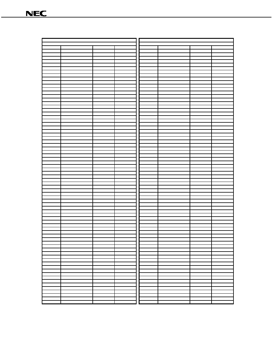
Table 2-1. Pad Layout (1/3)
PADTYPE : BUMP SIZE 100
µ
m x 40
µ
m
PADTYPE : BUMP SIZE 100
µ
m x 40
µ
m
GATE INPUTS
GATE INPUTS
PAD No.
PAD NAME
X [mm]
Y [mm]
PAD No.
PAD NAME
X [mm]
Y [mm]
1
DUMMY
-1.242
-4.5500
73
C2+
-1.242
-0.0300
2
TESTOUT2
-1.242
-4.4900
74
C2+
-1.242
0.0300
3
TESTIN2
-1.242
-4.4300
75
C2+
-1.242
0.0900
4
TESTIN1
-1.242
-4.3700
76
C1-
-1.242
0.1600
5
TESTOUT1
-1.242
-4.3100
77
C1-
-1.242
0.2200
6
PVCC1
-1.242
-4.2500
78
C1-
-1.242
0.2800
7
DUPF0
-1.242
-4.1900
79
C1-
-1.242
0.3400
8
PUPT0
-1.242
-4.1300
80
C1+
-1.242
0.4100
9
SCN2
-1.242
-4.0700
81
C1+
-1.242
0.4700
10
SCN1
-1.242
-4.0100
82
C1+
-1.242
0.5300
11
SCN0
-1.242
-3.9500
83
C1+
-1.242
0.5900
12
ACS0
-1.242
-3.8900
84
VDD2
-1.242
0.6600
13
EXRV
-1.242
-3.8300
85
VDD2
-1.242
0.7200
14
VSEL
-1.242
-3.7700
86
VDD2
-1.242
0.7800
15
CLS0
-1.242
-3.7100
87
VDD2
-1.242
0.8400
16
FS2
-1.242
-3.6500
88
VSS1
-1.242
0.9100
17
FS0
-1.242
-3.5900
89
VSS1
-1.242
0.9700
18
VMS
-1.242
-3.5300
90
VSS1
-1.242
1.0300
19
RGONR
-1.242
-3.4700
91
VSS1
-1.242
1.0900
20
PVSS1
-1.242
-3.4100
92
DUMMY
-1.242
1.1600
21
PVSS3
-1.242
-3.3500
93
VDC
-1.242
1.2300
22
VMON
-1.242
-3.2900
94
VDC
-1.242
1.2900
23
DUMMY
-1.242
-3.2300
95
VDC
-1.242
1.3500
24
PVCC1
-1.242
-3.1700
96
VDC
-1.242
1.4100
25
R,/L
-1.242
-3.1100
97
VDC
-1.242
1.4700
26
IFSEL
-1.242
-3.0500
98
VDC
-1.242
1.5300
27
PVSS1
-1.242
-2.9900
99
VDC
-1.242
1.5900
28
VCOMIN
-1.242
-2.9200
100
VDC
-1.242
1.6500
29
VCOM
-1.242
-2.8500
101
VCC1
-1.242
1.7200
30
VCOM
-1.242
-2.7900
102
VCC1
-1.242
1.7800
31
VCOM
-1.242
-2.7300
103
VCC1
-1.242
1.8400
32
COML
-1.242
-2.6600
104
VCC1
-1.242
1.9000
33
COML
-1.242
-2.6000
105
VSS1
-1.242
1.9700
34
COMH
-1.242
-2.5300
106
VSS1
-1.242
2.0300
35
COMH
-1.242
-2.4700
107
VSS1
-1.242
2.0900
36
VM
-1.242
-2.4000
108
VSS1
-1.242
2.1500
37
VM
-1.242
-2.3400
109
VSS1
-1.242
2.2100
38
VB
-1.242
-2.2700
110
VSS1
-1.242
2.2700
39
VB
-1.242
-2.2100
111
VR
-1.242
2.3400
40
VSS3
-1.242
-2.1400
112
VR
-1.242
2.4000
41
VSS3
-1.242
-2.0800
113
VR
-1.242
2.4600
42
VSS3
-1.242
-2.0200
114
VGD
-1.242
2.5300
43
VSS4
-1.242
-1.9500
115
VGD
-1.242
2.5900
44
VSS4
-1.242
-1.8900
116
VGD
-1.242
2.6500
45
VSS4
-1.242
-1.8300
117
MVS
-1.242
2.7200
46
VSS2
-1.242
-1.7600
118
VS
-1.242
2.7900
47
VSS2
-1.242
-1.7000
119
VS
-1.242
2.8500
48
VSS2
-1.242
-1.6400
120
VS
-1.242
2.9100
49
C6-
-1.242
-1.5700
121
VS
-1.242
2.9700
50
C6-
-1.242
-1.5100
122
VS
-1.242
3.0300
51
C6+
-1.242
-1.4400
123
VS
-1.242
3.0900
52
C6+
-1.242
-1.3800
124
DUMMY
-1.242
3.1600
53
C5-
-1.242
-1.3100
125
PVCC1
-1.242
3.2300
54
C5-
-1.242
-1.2500
126
VCD2
-1.242
3.3000
55
C5+
-1.242
-1.1800
127
RGON
-1.242
3.3700
56
C5+
-1.242
-1.1200
128
DCON
-1.242
3.4400
57
C4-
-1.242
-1.0500
129
FRM
-1.242
3.5100
58
C4-
-1.242
-0.9900
130
VCIN
-1.242
3.5800
59
C4+
-1.242
-0.9200
131
PVSS1
-1.242
3.6500
60
C4+
-1.242
-0.8600
132
/GRESET
-1.242
3.7200
61
C3-
-1.242
-0.7900
133
GCS
-1.242
3.7900
62
C3-
-1.242
-0.7300
134
GCL
-1.242
3.8600
63
C3+
-1.242
-0.6600
135
GDA
-1.242
3.9300
64
C3+
-1.242
-0.6000
136
STVR
-1.242
4.0000
65
VDD1
-1.242
-0.5300
137
STVL
-1.242
4.0700
66
VDD1
-1.242
-0.4700
138
DCCLK
-1.242
4.1400
67
VDD1
-1.242
-0.4100
139
CLK
-1.242
4.2100
68
C2-
-1.242
-0.3400
140
OE1
-1.242
4.2800
69
C2-
-1.242
-0.2800
141
OE2
-1.242
4.3500
70
C2-
-1.242
-0.2200
142
DUMMY
-1.242
4.4200
71
C2-
-1.242
-0.1600
143
VSS3
-1.242
4.4900
72
C2+
-1.242
-0.0900
144
DUMMY
-1.242
4.5600
Preliminary Product Information S15797EJ1V4PM
8
µ
µ
µ
µ
PD161644
Table 2-1. Pad Layout (2/3)
PADTYPE : BUMP SIZE 86
µ
m x 35
µ
m
PADTYPE : BUMP SIZE 86
µ
m x 35
µ
m
GATE OUTPUTS 35
µ
m pitch
GATE OUTPUTS 35
µ
m pitch
PAD No.
PAD NAME
X [mm]
Y [mm]
PAD No.
PAD NAME
X [mm]
Y [mm]
145
DUMMY
1.249
4.3050
217
O172
1.249
1.7850
146
DUMMY
1.127
4.2700
218
O171
1.127
1.7500
147
DUMMY
1.249
4.2350
219
O170
1.249
1.7150
148
O241
1.127
4.2000
220
O169
1.127
1.6800
149
O240
1.249
4.1650
221
O168
1.249
1.6450
150
O239
1.127
4.1300
222
O167
1.127
1.6100
151
O238
1.249
4.0950
223
O166
1.249
1.5750
152
O237
1.127
4.0600
224
O165
1.127
1.5400
153
O236
1.249
4.0250
225
O164
1.249
1.5050
154
O235
1.127
3.9900
226
O163
1.127
1.4700
155
O234
1.249
3.9550
227
O162
1.249
1.4350
156
O233
1.127
3.9200
228
O161
1.127
1.4000
157
O232
1.249
3.8850
229
O160
1.249
1.3650
158
O231
1.127
3.8500
230
O159
1.127
1.3300
159
O230
1.249
3.8150
231
O158
1.249
1.2950
160
O229
1.127
3.7800
232
O157
1.127
1.2600
161
O228
1.249
3.7450
233
O156
1.249
1.2250
162
O227
1.127
3.7100
234
O155
1.127
1.1900
163
O226
1.249
3.6750
235
O154
1.249
1.1550
164
O225
1.127
3.6400
236
O153
1.127
1.1200
165
O224
1.249
3.6050
237
O152
1.249
1.0850
166
O223
1.127
3.5700
238
O151
1.127
1.0500
167
O222
1.249
3.5350
239
O150
1.249
1.0150
168
O221
1.127
3.5000
240
O149
1.127
0.9800
169
O220
1.249
3.4650
241
O148
1.249
0.9450
170
O219
1.127
3.4300
242
O147
1.127
0.9100
171
O218
1.249
3.3950
243
O146
1.249
0.8750
172
O217
1.127
3.3600
244
O145
1.127
0.8400
173
O216
1.249
3.3250
245
O144
1.249
0.8050
174
O215
1.127
3.2900
246
O143
1.127
0.7700
175
O214
1.249
3.2550
247
O142
1.249
0.7350
176
O213
1.127
3.2200
248
O141
1.127
0.7000
177
O212
1.249
3.1850
249
O140
1.249
0.6650
178
O211
1.127
3.1500
250
O139
1.127
0.6300
179
O210
1.249
3.1150
251
O138
1.249
0.5950
180
O209
1.127
3.0800
252
O137
1.127
0.5600
181
O208
1.249
3.0450
253
O136
1.249
0.5250
182
O207
1.127
3.0100
254
O135
1.127
0.4900
183
O206
1.249
2.9750
255
O134
1.249
0.4550
184
O205
1.127
2.9400
256
O133
1.127
0.4200
185
O204
1.249
2.9050
257
O132
1.249
0.3850
186
O203
1.127
2.8700
258
O131
1.127
0.3500
187
O202
1.249
2.8350
259
O130
1.249
0.3150
188
O201
1.127
2.8000
260
O129
1.127
0.2800
189
O200
1.249
2.7650
261
O128
1.249
0.2450
190
O199
1.127
2.7300
262
O127
1.127
0.2100
191
O198
1.249
2.6950
263
O126
1.249
0.1750
192
O197
1.127
2.6600
264
O125
1.127
0.1400
193
O196
1.249
2.6250
265
O124
1.249
0.1050
194
O195
1.127
2.5900
266
O123
1.127
0.0700
195
O194
1.249
2.5550
267
O122
1.249
0.0350
196
O193
1.127
2.5200
268
O121
1.127
0.0000
197
O192
1.249
2.4850
269
O120
1.249
-0.0350
198
O191
1.127
2.4500
270
O119
1.127
-0.0700
199
O190
1.249
2.4150
271
O118
1.249
-0.1050
200
O189
1.127
2.3800
272
O117
1.127
-0.1400
201
O182
1.249
2.3450
273
O116
1.249
-0.1750
202
O187
1.127
2.3100
274
O115
1.127
-0.2100
203
O186
1.249
2.2750
275
O114
1.249
-0.2450
204
O185
1.127
2.2400
276
O113
1.127
-0.2800
205
O184
1.249
2.2050
277
O112
1.249
-0.3150
206
O183
1.127
2.1700
278
O111
1.127
-0.3500
207
O182
1.249
2.1350
279
O110
1.249
-0.3850
208
O181
1.127
2.1000
280
O109
1.127
-0.4200
209
O180
1.249
2.0650
281
O108
1.249
-0.4550
210
O179
1.127
2.0300
282
O107
1.127
-0.4900
211
O178
1.249
1.9950
283
O106
1.249
-0.5250
212
O177
1.127
1.9600
284
O105
1.127
-0.5600
213
O176
1.249
1.9250
285
O104
1.249
-0.5950
214
O175
1.127
1.8900
286
O103
1.127
-0.6300
215
O174
1.249
1.8550
287
O102
1.249
-0.6650
216
O173
1.127
1.8200
288
O101
1.127
-0.7000

Preliminary Product Information S15797EJ1V4PM
9
µ
µ
µ
µ
PD161644
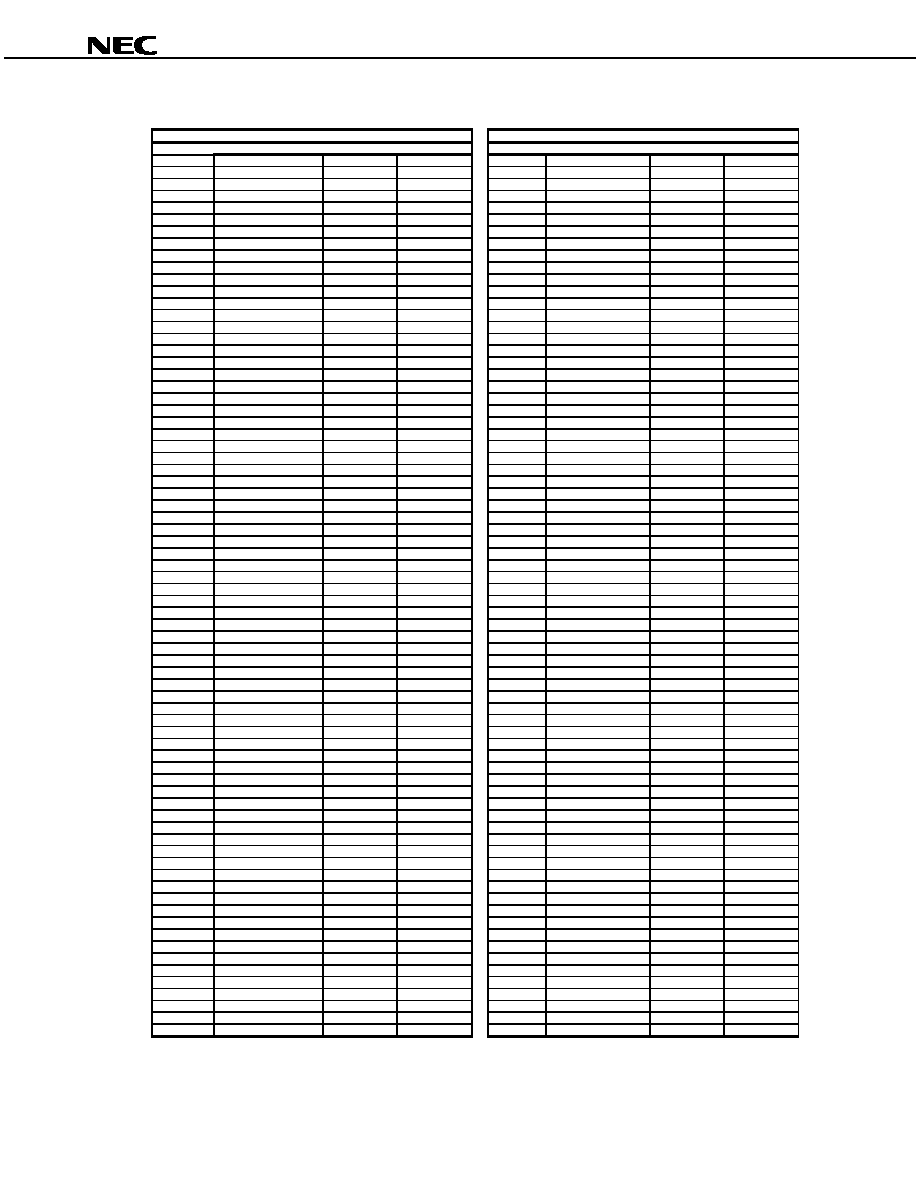
Table 2-1. Pad Layout (3/3)
PADTYPE : BUMP SIZE 86
µ
m x 35
µ
m
PADTYPE : BUMP SIZE 86
µ
m x 35
µ
m
GATE OUTPUTS 35
µ
m pitch
GATE OUTPUTS 35
µ
m pitch
PAD No.
PAD NAME
X [mm]
Y [mm]
PAD No.
PAD NAME
X [mm]
Y [mm]
289
O100
1.249
-0.7350
361
O28
1.249
-3.2550
290
O99
1.127
-0.7700
362
O27
1.127
-3.2900
291
O98
1.249
-0.8050
363
O26
1.249
-3.3250
292
O97
1.127
-0.8400
364
O25
1.127
-3.3600
293
O96
1.249
-0.8750
365
O24
1.249
-3.3950
294
O95
1.127
-0.9100
366
O23
1.127
-3.4300
295
O94
1.249
-0.9450
367
O22
1.249
-3.4650
296
O93
1.127
-0.9800
368
O21
1.127
-3.5000
297
O92
1.249
-1.0150
369
O20
1.249
-3.5350
298
O91
1.127
-1.0500
370
O19
1.127
-3.5700
299
O90
1.249
-1.0850
371
O18
1.249
-3.6050
300
O89
1.127
-1.1200
372
O17
1.127
-3.6400
301
O88
1.249
-1.1550
373
O16
1.249
-3.6750
302
O87
1.127
-1.1900
374
O15
1.127
-3.7100
303
O86
1.249
-1.2250
375
O14
1.249
-3.7450
304
O85
1.127
-1.2600
376
O13
1.127
-3.7800
305
O84
1.249
-1.2950
377
O12
1.249
-3.8150
306
O83
1.127
-1.3300
378
O11
1.127
-3.8500
307
O82
1.249
-1.3650
379
O10
1.249
-3.8850
308
O81
1.127
-1.4000
380
O9
1.127
-3.9200
309
O80
1.249
-1.4350
381
O8
1.249
-3.9550
310
O79
1.127
-1.4700
382
O7
1.127
-3.9900
311
O78
1.249
-1.5050
383
O6
1.249
-4.0250
312
O77
1.127
-1.5400
384
O5
1.127
-4.0600
313
O76
1.249
-1.5750
385
O4
1.249
-4.0950
314
O75
1.127
-1.6100
386
O3
1.127
-4.1300
315
O74
1.249
-1.6450
387
O2
1.249
-4.1650
316
O73
1.127
-1.6800
388
O1
1.127
-4.2000
317
O72
1.249
-1.7150
389
DUMMY
1.249
-4.2350
318
O71
1.127
-1.7500
390
DUMMY
1.127
-4.2700
319
O70
1.249
-1.7850
391
DUMMY
1.249
-4.3050
320
O69
1.127
-1.8200
321
O68
1.249
-1.8550
322
O67
1.127
-1.8900
323
O66
1.249
-1.9250
324
O65
1.127
-1.9600
325
O64
1.249
-1.9950
326
O63
1.127
-2.0300
327
O62
1.249
-2.0650
328
O61
1.127
-2.1000
329
O60
1.249
-2.1350
330
O59
1.127
-2.1700
331
O58
1.249
-2.2050
332
O57
1.127
-2.2400
333
O56
1.249
-2.2750
334
O55
1.127
-2.3100
335
O54
1.249
-2.3450
336
O53
1.127
-2.3800
337
O52
1.249
-2.4150
338
O51
1.127
-2.4500
339
O50
1.249
-2.4850
340
O49
1.127
-2.5200
341
O48
1.249
-2.5550
342
O47
1.127
-2.5900
343
O46
1.249
-2.6250
344
O45
1.127
-2.6600
345
O44
1.249
-2.6950
346
O43
1.127
-2.7300
347
O42
1.249
-2.7650
348
O41
1.127
-2.8000
349
O40
1.249
-2.8350
350
O39
1.127
-2.8700
351
O38
1.249
-2.9050
352
O37
1.127
-2.9400
353
O36
1.249
-2.9750
354
O35
1.127
-3.0100
355
O34
1.249
-3.0450
356
O33
1.127
-3.0800
357
O32
1.249
-3.1150
358
O31
1.127
-3.1500
359
O30
1.249
-3.1850
360
O29
1.127
-3.2200

Preliminary Product Information S15797EJ1V4PM
10
µ
µ
µ
µ
PD161644
3. PIN FUNCTIONS
(1/5)
Symbol
Pin Name
Pad No.
I/O
Function
V
DC
DC/DC converter
reference voltage
93 to 100
-
Reference voltage input pin for DC/DC converter.
V
CC1
Logic reference
voltage
101 to 104
-
2.5 to 3.3 V LS (level shifter) reference voltage input pin.
V
SS1
Ground
88 to 91,
105 to 110
-
Connect to the system ground.
VGD
Power supply input
for DC/DC converter
114 to 116
Input
Reference voltage input pin for V
DD1
, V
SS1
to V
SS4
boost.
Connect to any of V
DD2,
V
R
or V
S
.
V
DD1
DC/DC converter
output
65 to 67
Output
Boost output voltage of DC/DC converter (VGD x 2 or x 3).
The boost step number of V
DD1
is selected according to how the
external capacitor is connected. The boost reference voltage can
be set using VGD. Refer to the function of VGD pin.
V
DD2
DC/DC converter
output
84 to 87
Output
Boost output voltage of DC/DC converter (V
DC
x 2 or x 3). The
boost step number of V
DD2
can be set using VCD2.
V
SS2
DC/DC converter
output
46 to 48
Output
Boost output voltage of DC/DC converter (VGD x
-
1 or x
-
2).
The boost step number of V
SS2
is selected according to how the
external capacitor is connected. The boost reference voltage can
be set using VGD. Refer to the function of VGD pin.
V
SS3
DC/DC converter
output
40 to 42, 143
Output
Boost output voltage of DC/DC converter (VGD
x
-
2 or x
-
3).
The boost step number of V
SS3
is selected according to how the
external capacitor is connected. The boost reference voltage can
be set using VGD. Refer to VGD pin function.
V
SS4
DC/DC converter
output
43 to 45
Output
Boost output voltage of DC/DC converter (V
DC
x
-
1).
VM
Gate output low
level select voltage
36, 37
Output
The voltage level of V
SS2
or V
SS3
is output synchronized with the
VCIN input.
VCIN = 0: Output the voltage level of V
SS3
VCIN = 1: Output the voltage level of V
SS2
The timing chart is shown in Figure 3-1.
V
B
Driver negative
voltage
38, 39
Input
Negative voltage of output buffer. This is the input pin of the
liquid crystal driver negative voltage. Input the negative power
supply of the gate output. V
B
pin connection examples are
shown in Figure 3-2.
C
1
+
, C
1
-
C
2
+
, C
2
-
C
3
+
, C
3
-
C
4
+
, C
4
-
C
5
+
, C
5
-
C
6
+
, C
6
-
Capacitor connect
pin for boost
80 to 83, 76 to 79,
72 to 75, 68 to 71,
63, 64, 61, 62,
59, 60, 57, 58,
55, 56, 53, 54,
51, 52, 49, 50
Output
To connect booster for DC/DC converter.
For the recommended values of the capacitance and
withstanding voltage of each capacitor, refer to
9. RECOMMENDED CAPACITANCE VALUES OF EXTERNAL
CAPACITOR.
V
R
Power supply
output for DC/DC
converter
111 to 113
Output
Positive power supply voltage output for the DC/DC converter.
The V
R
output voltage can be changed by setting VRSEL0 to
VRSEL2.
Preliminary Product Information S15797EJ1V4PM
11
µ
µ
µ
µ
PD161644
(2/5)
Symbol
Pin Name
Pad No.
I/O
Function
V
S
Positive power
output supply for
driver
118 to 123
Output
Positive power supply voltage output for source driver. The V
S
output voltage can be changed by setting VSEL0 to VSEL2.
MVS
External resistor
input
117
Input
Any output voltage can be set by connecting an external resistor.
<EXRV = 0> Leave open.
<EXRV = 1> Connect to external resistor.
PV
CC1
Pull-up voltage
6, 24, 125
-
Pull-up voltage for mode setting pin.
PV
SS1
Pull-down voltage
20, 27, 131
-
Pull-down voltage for mode setting pin.
PV
SS3
Pull-down voltage
21
-
Pull-down voltage for mode setting pin.
CLK
Shift clock input
139
Input
Shift clock input pin of the internal shift resistor. The contents of
internal shift resistor are shifted at the rising edge of CLK.
Connect to GCLK pin of source driver.
STVR,
STVL
Start pulse
input/output pin
136,
137
I/O
Input/output pin of the internal shift resistor.
Start pulse signal is read at the rising edge of shift clock CLK and a
scan signal is output from the driver output pin.
The valid level of the STVR/STVL pin is determined by the setting
of STVSEL.
When STVSEL = L, the pulse becomes low level at the falling
edge of the 240th shift clock CLK and high level at falling edge of
the 241st clock.
OE
1
Enable input
140
Input
If the level selected by OE1SEL is input, the driver output is fixed to
low level (When OE1SEL = L the driver output is fixed to low level if
a low level is input). However, the shift resistor is not cleared. And,
output enable actuation is asynchronous in the clock.
Connect to GOE
1
pin of source driver.
OE
2
Enable input
141
Input
If the level selected by OE2SEL is input, the driver output is fixed to
high level (When OE2SEL = L the driver output is fixed to low level
if a high level is input). However, the shift resistor is not cleared.
And, output enable actuation is asynchronous in the clock.
Connect to GOE
2
pin of source driver.
R,/L
Shift direction
control
25
Input
The shift direction control pin of shift register. The shift directions
of the shift registers are as follows.
R,/L = H (right shift): STVR input, O
1
O
241
,
STVL output
R,/L = L (left shift) : STVL input, O
241
O
1
,
STVR output
FRM
Frame signal input
129
Input
Input frame reverse signals.
Connect to GFRAME pin of source driver.
DCCLK
Clock input for
DC/DC converter
138
Input
To input the external clock for the DC/DC converter.
This pin is valid only when CLS0 = 1 and CLS1 = 1. In other
settings, leave open.
Preliminary Product Information S15797EJ1V4PM
12
µ
µ
µ
µ
PD161644
(3/5)
Symbol
Pin Name
Pad No.
I/O
Function
O
1
to O
241
Driver output pins
388 to 148
Output
Scan signal output pins that drive the gate electrode of a TFT-
LCD. The status of each output pin changes in synchronization
with the rising edge of shift clock CLK. The output voltage of the
driver is V
DD1
to V
B
.
COMH
Common high level
output
34, 35
Output
<COMON = 1> High level of common voltage is output. The voltage
level changes accordance with DA
0
to DA
7
and CDA
0
to CDA
7
.
<COMON = 0> Leave open when not using it.
COML
Common low level
output
32, 33
Output
<COMON = 1> Low level of common voltage is output. The voltage
level changes accordance with DA
0
to DA
7
and CDA
0
to CDA
7
.
<COMON = 0> Leave open when not using it.
VCOM
Common output
29 to 31
Output
<COMON = 1> The common voltage synchronized with the VCIN
input is output.
Connect to common pin of panel.
<COMON = 0> Leave open when not using it.
VCOMIN
VCOM center
voltage input
28
Input
VCOM center voltage input pin. Leave open when COMSEL = 0.
<COMSEL = 0> Internal D/A is valid.
<COMSEL = 1> VCOMIN input voltage is valid.
VCIN
Common pulse
input
130
Input
To input common pulse. Connect to VCOUT3 pin of source driver.
Fix this pin to low when not using it.
/GRESET
Reset input
132
Input
Reset input pin. Connect to /GRESET pin of source driver.
If /GRESET is made low, the serial interface is initialized (the
register values are not initialized). A reset operation is executed
according to the level of the /GRESET signal. Be sure to execute
a reset using this pin at power application.
IFSEL
Interface selection
26
Input
The serial interface input switching pin.
<IFSEL = 0> Serial interface input.
The DCON, RGONR, VCD2, VMS, FS0, FS2, CLS0, RGON, VSEL,
EXRV, ACS0, SCN0 to SCN2, PUPT0, DUPF0 pins should be left
open.
<IFSEL = 1> Control pin input.
The GCS, GCL, GDA pins should be left open.
GCS
Chip select input
133
Input
<IFSEL = 0> To input chip select signals.
Connect to GCS pin of source driver.
<IFSEL = 1> Leave open.
GCL
Serial clock input
134
Input
<IFSEL = 0> To input serial clock signals.
Connect to GCL pin of source driver.
<IFSEL = 1> Leave open.
GDA
Serial data input
135
Input
<IFSEL = 0> To input serial data signals.
Connect to GDA pin of source driver.
<IFSEL = 1> Leave open.

Preliminary Product Information S15797EJ1V4PM
13
µ
µ
µ
µ
PD161644
(4/5)
Symbol
Pin Name
Pad No.
I/O
Function
DCON
DC/DC converter
control
128
Input
<IFSEL = 0> Leave open (Internal resistors are valid).
<IFSEL = 1> The DC/DC converter ON/OFF control signal is input.
Connect to the DCON pin of the source driver.
<DCON = 0> DC/DC converter OFF
<DCON = 1> DC/DC converter ON
RGONR
V
R
regulator control 19
Input
<IFSEL = 0> Leave open (Internal resistors are valid).
<IFSEL = 1> The V
R
regulator ON/OFF control signal is input.
<RGONR = 0> V
R
regulator OFF
<RGONR = 1> V
R
regulator ON
VCD2
V
DD2
boost
selection
126
Input
<IFSEL = 0> Leave open (Internal resistors are valid).
<IFSEL = 1> The V
DD2
boost step number select pin.
<VCD2 = 0> V
DD2
= V
DC
x 2
<VCD2 = 1> V
DD2
= V
DC
x 3
VMS
V
DD2
boost
selection
18
Input
<IFSEL = 0> Leave open (Internal resistors are valid).
<IFSEL = 1> V
DD2
boost mode select pin.
<VMS = 0> V
DD2
: single boost mode
<VMS = 1> V
DD2
: dual boost mode
FS0
V
DD2,
V
SS4
boost
frequency selection
in scan mode
17
Input
<IFSEL = 0> Leave open (Internal resistors are valid).
<IFSEL = 1> V
DD2
,
V
SS4
boost frequency select pin in scan mode.
<FS0 = 0 > f
OSC
/2
<FS0 = 1 > f
OSC
/4
FS2
V
DD1
, V
SS2
, V
SS3
boost frequency
selection in scan
mode
16
Input
<IFSEL = 0> Leave open (Internal resistors are valid).
<IFSEL = 1> V
DD1
, V
SS2
, V
SS3
boost frequency select pin
in scan
mode.
<FS2 = 0 > f
OSC
/2
<FS2 = 1, > f
OSC
/4
CLS0
DC/DC OSC
frequency selection
15
Input
<IFSEL = 0> Leave open (Internal resistors are valid).
<IFSEL = 1> Select pin of the OSC oscillation frequency for DC/DC
converter.
<CLS0 = 0> f
OSC
= 25 kHz, DCCLK: Open
<CLS0 = 1> External CK input mode
RGON
V
S
regulator control 127
Input
<IFSEL = 0> Leave open (Internal resistors are valid).
<IFSEL = 1> The V
S
regulator ON/OFF control signal is input.
Connect this pin to the RGON pin of the source driver.
<RGON = 0> V
S
regulator OFF
<RGON = 1> V
S
regulator ON
VSEL
V
S
regulator voltage
selection
14
Input
<IFSEL = 0> Leave open (Internal resistors are valid).
<IFSEL = 1> Select pin of output voltage for V
S
regulator.
<VSEL = 1> V
S
= 4 V
<VSEL = 0> V
S
= 5 V
EXRV
V
S
regulating resistor
selection
13
Input
<IFSEL = 0> Leave open (Internal resistors are valid).
<IFSEL = 1> Select pin of external resistor for V
S
regulator.
<EXRV = 0> Internal resistor setting mode.
<EXRV = 1> Any output voltage can be set by connecting MVS to
an external resistor.

Preliminary Product Information S15797EJ1V4PM
14
µ
µ
µ
µ
PD161644
(5/5)
Symbol
Pin Name
Pad No.
I/O
Function
ACS0
Amp. current
selection in scan
mode
12
Input
<IFSEL = 0> Leave open (Internal resistors are valid).
<IFSEL = 1> Amp. current select pin in scan mode.
<ACS0 = 0> Amp. current = 5
µ
A
<ACS0 = 1> Amp. current = 15
µ
A
SCN0,
SCN1,
SCN2
Gate scan selection
11,
10,
9
Input
<IFSEL = 0> Leave open (Internal resistors are valid).
<IFSEL = 1> Select pin of gate scan order.
<SCN0 = 1, SCN1 = 1, SCN2 = 1> MODE1
<SCN0 = 1, SCN1 = 1, SCN2 = 0> MODE2
<SCN0 = 1, SCN1 = 0, SCN2 = 1> MODE3
<SCN0 = 1, SCN1 = 0, SCN2 = 0> MODE4
<SCN0 = 0, SCN1, SCN2 = x> MODE5
PUPT0
Setting pin of
DC/DC converter
power on time
8
Input
<IFSEL = 0> Leave open (Internal resistors are valid).
<IFSEL = 1> This pin sets the rising time of V
DD1
, V
DD2
, V
SS2
to
V
SS4
at DC/DC converter power on time.
DUPF0
Operating frequency
setting pin at
DC/DC converter
power on
7
Input
<IFSEL = 0> Leave open (Internal resistors are valid).
<IFSEL = 1> This pin sets the operating frequency at DC/DC
converter power on time.
<DUPT0 = 0> f
OSC
/8
<DUPT0 = 1> f
OSC
/16
VMON
Stand-by current
reduction control
pin
22
Input
The standby current reduction control pin.
<VMON = PV
SS3
> Normal mode.
A quiescent current of about 0.5
µ
A is consumed in standby mode.
When the V
CC1
voltage drops, the driver output pins are fixed to
ALL-High.
<VMON = PV
CC1
> Standby current reduction mode.
Makes the quiescent current consumed in standby mode 0.
When the V
CC1
voltage drops, the driver output pins are undefined.
TESTOUT1
V
REF
reference
voltage output
5
Output
The V
REF
voltage measurement pin. Leave open.
TESTIN1,
TESTIN2
TEST input pin
4,
3
Input
Test input pins. Leave open.
TESTOUT2
TEST output pin
2
Output
Test output pin. Leave open.
DUMMY
Dummy
1, 23, 92, 124,
142, 144 to 147,
389 to 391
-
Dummy data

Preliminary Product Information S15797EJ1V4PM
15
µ
µ
µ
µ
PD161644
Figure 3-1. VM signal Timing Chart
V
SS
V
CC1
V
SS
V
CC1
V
SS
V
CC1
V
SS
V
CC1
GOE1ON(R59) = "1"
DC/DC converter ON
CLK = "H" + OE
1
= "L" : Hi-Z
CLK = "H": Hi-Z
Output Hi-Z term
V
SS
V
CC1
Remark Hi-Z (High impedance)
Figure 3-2. Examples of V
B
pin connection
(a) When the negative voltage level of the gate output
is set to V
SS3
Lev
el
s
h
i
f
t
e
r
VCIN
VM
V
B
O
1
O
2
O
241
V
SS2
V
SS3
V
DD1
to Panel gate line
µ
µ
µ
µ
PD161644
DC/DC converter
V
SS2
V
SS3
VGD
V
DD1
open
V
S
or V
R
open
(b) When the negative voltage level of the gate output
is switched between V
SS2
and V
SS3
Lev
el
s
h
i
f
t
e
r
VCIN
VM
V
B
O
1
O
2
O
241
V
SS2
V
SS3
V
DD1
to Panel gate line
µ
µ
µ
µ
PD161644
DC/DC converter
V
SS2
V
SS3
VGD
V
DD1
VCOUT3
V
S
or
V
R
common
driving signal
from
µ
PD161621

Preliminary Product Information S15797EJ1V4PM
16
µ
µ
µ
µ
PD161644
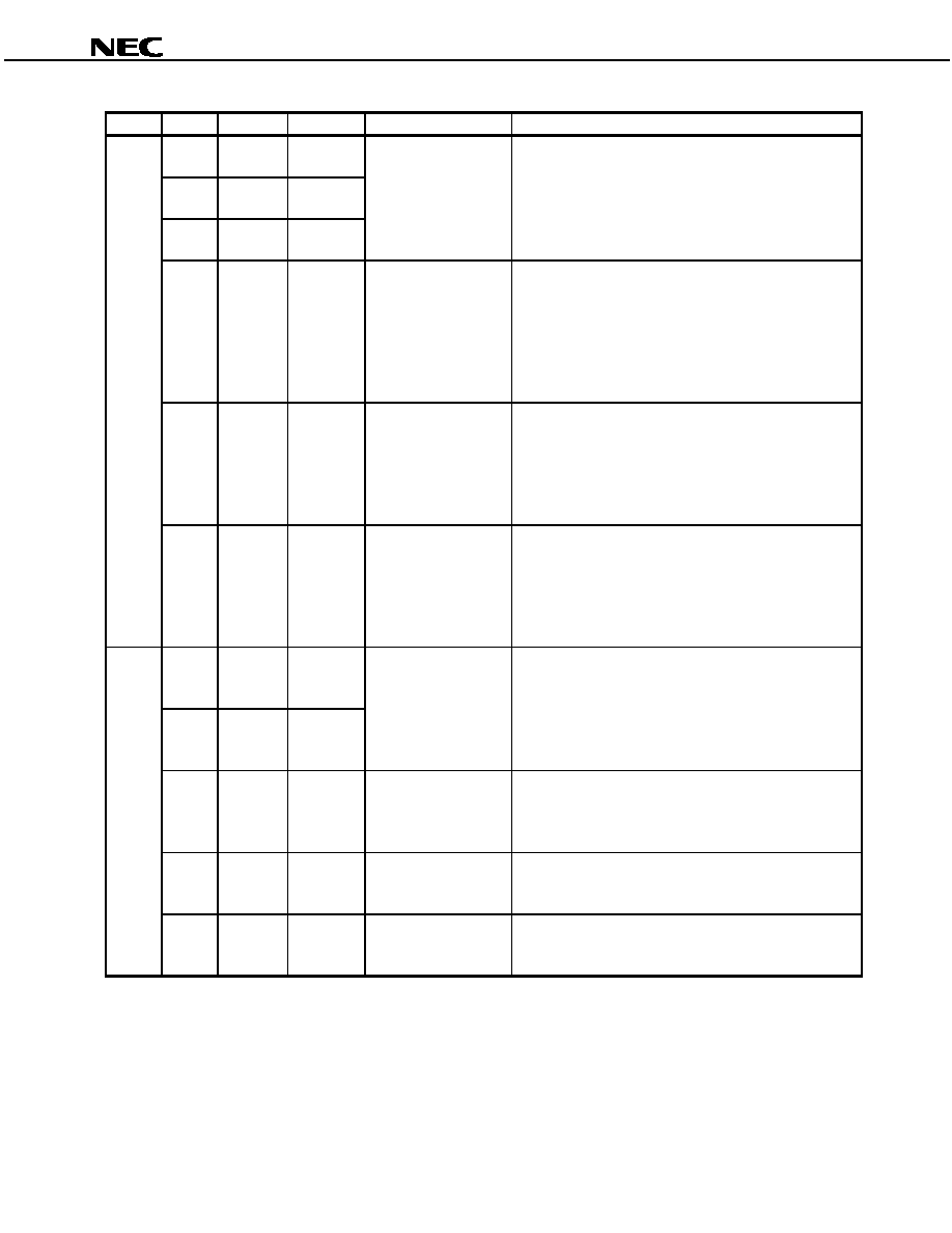
4. COMMAND
4.1 Command List
Data bit
7 6 5 4 3 2 1 0
Rn
Register
D
7
D
6
D
5
D
4
D
3
D
2
D
1
D
0
0 0 0 1 1 0 0 0 R24 DC/DC operation setting
RGONR VS4ON VS3ON VS2ON VD2ON VD1ON DCON
0 0 0 1 1 0 0 1 R25 DC/DC step setting
VRSEL2VRSEL1 VRSEL0 VMS
VCD2
0 0 0 1 1 0 1 0 R26 DC/DC oscillation setting
FUP
CLS1
CLS0
FS3
FS2
FS1
FS0
0 0 0 1 1 0 1 1 R27
Regulator output setting
ACS1
ACS0
EXRV VSEL2
VSEL1 VSEL0 RGON
0 0 0 1 1 1 0 0 R28 LPM setting
LACS1 LACS0
LFS3
LFS2
LFS1
LFS0
LPM
0 0 0 1 1 1 0 1 R29 Gate scan setting
OE2SEL OE1SELSTVSEL SCN2
SCN1
SCN0
0 0 0 1 1 1 1 0 R30 Gate mode setting
COMHI
COMSEL
COMON NLINE2 NLINE1
0 0 0 1 1 1 1 1 R31 Common amplitude setting
DA
7
DA
6
DA
5
DA
4
DA
3
DA
2
DA
1
DA
0
0 0 1 0 0 0 0 0 R32 Common center setting
CDA
7
CDA
6
CDA
5
CDA
4
CDA
3
CDA
2
CDA
1
CDA
0
0 0 1 0 0 0 0 1 R33 DC/DC power on setting
PONM
PON
DUPF1 DUPF0 PUPT1 PUPT0
0 0 1 0 0 0 1 0 R34 Reset
RES
4.2 Command Description
Reset the internal data at power application by inputting a low level to the /GRESET pin.
(1/5)
Resistor
Bit
Symbol
Reset
Function
Description
R24
D
0
DCON
0
DC/DC converter control
Control ON/OFF of DC/DC converter.
<DCON = 0> DC/DC converter OFF
<DCON = 1> DC/DC converter ON
D
1
VD1ON
0
V
DD1
boost control
Control ON/OFF of V
DD1
boost.
<VD1ON = 0> V
DD1
boost OFF
<VD1ON = 1> V
DD1
boost ON
D
2
VD2ON
0
V
DD2
boost control
Control V
DD2
boost ON/OFF.
<VD2ON = 0> V
DD2
boost OFF
<VD2ON = 1> V
DD2
boost ON
D
3
VS2ON
0
V
SS2
boost control
Control
VSS2
boost ON/OFF.
<VS2ON = 0> V
SS2
boost OFF
<VS2ON = 1> V
SS2
boost ON
D
4
VS3ON
0
V
SS3
boost control
Control V
SS3
boost ON/OFF.
<VS3ON = 0> V
SS3
boost OFF
<VS3ON = 1> V
SS3
boost ON
D
5
VS4ON
0
V
SS4
boost control
Control V
SS4
boost ON/OFF.
<VS4ON = 0> V
SS4
boost OFF
<VS4ON = 1> V
SS4
boost ON
D
6
RGONR
0
V
R
regulator control
Control ON/OFF of V
R
regulator.
<RGONR = 0> V
R
regulator OFF
<RGONR = 1> V
R
regulator ON

Preliminary Product Information S15797EJ1V4PM
17
µ
µ
µ
µ
PD161644
(2/5)
Resistor
Bit
Symbol
Reset
Function
Description
R25
D
0
VCD2
0
V
DD2
boost selection
Select the number of V
DD2
boost step (x2/x3).
<VCD2 = 0> V
DD2
= V
DC
x 2
<VCD2 = 1> V
DD2
= V
DC
x 3
D
1
VMS
1
V
DD2
boost mode
selection
Select V
DD2
boost mode.
<VMS = 0> V
DD2
= Single boost mode
<VMS = 1> V
DD2
= Dual boost mode
D
2
VRSEL0
1
D
3
VRSEL1
0
D
4
VRSEL2
1
V
R
regulator output
voltage selection
Select output voltage of V
R
regulator. When IFSEL = 1, V
R
is fixed to 5 V.
<VRSEL0 = 0, VRSEL1 = 0, VRSEL2 = 0> V
R
= 3 V
<VRSEL0 = 1, VRSEL1 = 0, VRSEL2 = 0> V
R
= 3.5 V
<VRSEL0 = 0, VRSEL1 = 1, VRSEL2 = 0> V
R
= 4 V
<VRSEL0 = 1, VRSEL1 = 1, VRSEL2 = 0> V
R
= 4.5 V
<VRSEL0 = 0, VRSEL1 = 0, VRSEL2 = 1> V
R
= 4.75 V
<VRSEL0 = 1, VRSEL1 = 0, VRSEL2 = 1> V
R
= 5 V
<VRSEL0 = 0, VRSEL1 = 1, VRSEL2 = 1> V
R
= 5.25 V
<VRSEL0 = 1, VRSEL1 = 1, VRSEL2 = 1> V
R
= 5.5 V
D
0
FS0
1
R26
D
1
FS1
0
V
DD2
, V
SS4
boost
frequency selection in
scan mode
Select V
DD2,
V
SS4
boost frequency in scan mode. When
IFSEL = 1, FS1 is fixed to 0.
<FS0 = 0, FS1 = 0> f
OSC
/2 <FS0 = 1, FS1 = 0> f
OSC
/4
<FS0 = 0, FS1 = 1> f
OSC
/8 <FS0 = 1, FS1 = 1> f
OSC
/16
D
2
FS2
1
D
3
FS3
0
V
DD1
, V
SS2
, V
SS3
boost frequency
selection in scan mode
Select V
DD1
, V
SS2
, V
SS3
boost frequency in scan mode.
When IFSEL = 1, FS3 is fixed to 0.
<FS2 = 0, FS3 = 0> f
OSC
/2 <FS2 = 1, FS3 = 0> f
OSC
/4
<FS2 = 0, FS3 = 1> f
OSC
/8 <FS2 = 1, FS3 = 1> f
OSC
/16
D
4
CLS0
1
D
5
CLS1
0
DC/DC OSC frequency
selection
Select oscillation frequency of OSC for DC/DC converter.
When IFSEL = 1, CLS1 is fixed to 1.
<CLS0 = 0, CLS1 = 0> f
OSC
= 18 kHz, DCCLK: Open
<CLS0 = 1, CLS1 = 0> f
OSC
= 25 kHz, DCCLK: Open
<CLS0 = 0, CLS1 = 1> f
OSC
= 37 kHz, DCCLK: Open
<CLS0 = 1, CLS1 = 1> External CK input mode
D
6
FUP
0
Switching of DC/DC
OSC frequency
Select oscillation frequency of OSC for DC/DC converter.
When IFSEL = 1, the frequency is fixed to f
OSC
.
<FUP = 0> f
OSC
<FUP = 1> f
OSC
x 2

Preliminary Product Information S15797EJ1V4PM
18
µ
µ
µ
µ
PD161644
(3/5)
Resistor
Bit
Symbol
Reset
Function
Description
R27
D
0
RGON
0
V
S
regulator control
Control ON/OFF of V
S
regulator.
<RGON = 0> V
S
regulator OFF
<RGON = 1> V
S
regulator ON
D
1
VSEL0
1
D
2
VSEL1
0
D
3
VSEL2
1
V
S
regulator output
voltage selection
Select the output voltage of V
S
regulator.
VSEL0 = 0: V
S
= 5 V, VSEL = 1: V
S
= 4 V when IFSEL = 1.
<VSEL0 = 0, VSEL1 = 0, VSEL2 = 0> V
S
= 3 V
<VSEL0 = 1, VSEL1 = 0, VSEL2 = 0> V
S
= 3.5 V
<VSEL0 = 0, VSEL1 = 1, VSEL2 = 0> V
S
= 4 V
<VSEL0 = 1, VSEL1 = 1, VSEL2 = 0> V
S
= 4.5 V
<VSEL0 = 0, VSEL1 = 0, VSEL2 = 1> V
S
= 4.75 V
<VSEL0 = 1, VSEL1 = 0, VSEL2 = 1> V
S
= 5 V
<VSEL0 = 0, VSEL1 = 1, VSEL2 = 1> V
S
= 5.25 V
<VSEL0 = 1, VSEL1 = 1, VSEL2 = 1> V
S
= 5.5 V
D
4
EXRV
0
V
S
regulator resistor
selection
Select external resistor of V
S
regulator.
<EXRV = 0> Internal resistor mode
<EXRV = 1> Connect external resistor to MVS and set any
level of voltage
D
5
ACS0
0
D
6
ACS1
0
Amp. current selection
in scan mode
Select Amp. current of V
R
and V
S
regulators in scan mode.
When IFSEL = 1, ACS1 is fixed to 0.
<ACS0 = 0, ACS1 = 0> Amp. current = 5
µ
A
<ACS0 = 0, ACS1 = 1> Amp. current = 10
µ
A
<ACS0 = 1, ACS1 = 0> Amp. current = 15
µ
A
<ACS0 = 1, ACS1 = 1> Amp. current = 30
µ
A
R28
D
0
LPM
0
Low power mode
control
Control in low power mode. When IFSEL = 1, LPM is fixed
to 0.
<LPM = 0> Scan mode
<LPM = 1> Low power mode
D
1
LFS0
0
D
2
LFS1
0
V
DD2
, V
SS4
boost
frequency selection in
low power mode
Select boost frequency of V
DD2
, V
SS4
in low power mode.
<LFS0 = 0, LFS1 = 0> f
OSC
/8
<LFS0 = 1, LFS1 = 0> f
OSC
/16
<LFS0 = 0, LFS1 = 1> f
OSC
/32
<LFS0 = 1, LFS1 = 1> f
OSC
/64
D
3
LFS2
0
D
4
LFS3
0
V
DD1
, V
SS2
, V
SS3
boost frequency
selection in low power
mode
Select boost frequency of V
DD1,
V
SS2
, V
SS3
in low power
mode.
<LFS2 = 0, LFS3 = 0> f
OSC
/8
<LFS2 = 1, LFS3 = 0> f
OSC
/16
<LFS2 = 0, LFS3 = 1> f
OSC
/32
<LFS2 = 1, LFS3 = 1> f
OSC
/64
D
5
LACS0
0
D
6
LACS1
0
Amp. current selection
in low power mode
Select Amp. current in low power mode.
<LACS0 = 0, LACS1 = 0> Amp. current = 1.25
µ
A
<LACS0 = 0, LACS1 = 1> Amp. current = 2.5
µ
A
<LACS0 = 1, LACS1 = 0> Amp. current = 5
µ
A
<LACS0 = 1, LACS1 = 1> Amp. current = 7.5
µ
A
Preliminary Product Information S15797EJ1V4PM
19
µ
µ
µ
µ
PD161644
(4/5)
Resistor
Bit
Symbol
Reset
Function
Description
D
0
SCN0
1
D
1
SCN1
1
R29
D
2
SCN2
1
Gate scan selection
Select scan order of gate scan.
<SCN0 = 1, SCN1 = 1, SCN2 = 1> MODE1
<SCN0 = 1, SCN1 = 1, SCN2 = 0> MODE2
<SCN0 = 1, SCN1 = 0, SCN2 = 1> MODE3
<SCN0 = 1, SCN1 = 0, SCN2 = 0> MODE4
<SCN0 = 0, SCN1, SCN2 = X> MODE5
D
3
STVSEL
0
Start pulse input/output
valid level selection
Select start pulse input/output valid level to STVR/STVL.
But there is no pin to select start pulse input/output valid
level. When IFSEL = H (When using control pins), low-fixed
is valid. Refer to 4.3 Command Setting Values When
IFSEL = H (When Using Control Pins).
<STVSEL= 0> Low level is valid.
<STVSEL= 1> High level is valid.
D
4
OE1SEL
0
OE
1
valid level selection
Select valid level of OE
1
. But there is no pin to select valid
level of OE
1
. When IFSEL = H (When using control pins),
low-fixed is valid. Refer to 4.3 Command Setting Values
When IFSEL = H (When Using Control Pins).
<OE1SEL = 0> OE
1
= Low, gate output OFF
<OE1SEL = 1> OE
1
= High, gate output OFF
D
5
OE2SEL
0
OE
2
valid level selection
Select valid level of OE
2
. There is no pin to select valid
level of OE
2
. When IFSEL = H (When using control pins),
low-fixed is valid. Refer to 4.3 Command Setting Values
When IFSEL = H (When Using Control Pins).
<OE2SEL = 0> OE
2
= Low, gate output ON
<OE2SEL = 1> OE
2
= High, gate output ON
D
0
NLINE1
1
R30
D
1
NLINE2
1
Gate mode selection
Select 1-line skip, 2-line skip or N frame inversion of a gate
scan. When IFSEL = 1, this is fixed to normal mode.
<NLINE1 = 1, NLINE2 = 1> Normal mode
<NLINE1 = 1, NLINE2 = 0> 1-line skip mode
<NLINE1 = 0, NLINE2 = 1> 2-line skip mode
<NLINE1 = 0, NLINE2 = 0> N frame inversion
D
2
COMON
0
COM output control
Control ON/OFF of COM output. When IFSEL = 1, COMON
is fixed to 0.
<COMON = 0> COM_AMP, COM output OFF
<COMON = 1> COM_AMP, COM output ON
D
3
COMSEL
0
VCOM center input
selection
Select VCOM center voltage input.
<COMSEL = 0> Internal D/A is valid.
<COMSEL = 1> VCOMIN input voltage is valid.
D
4
COMHI
0
VCOM output selection
Select VCOM output.
<COMHI = 0> VCOM = Hi-Z
<COMHI = 1> VCOM = Output

Preliminary Product Information S15797EJ1V4PM
20
µ
µ
µ
µ
PD161644
(5/5)
Resistor
Bit
Symbol
Reset
Function
Description
R31
D
0
to D
7
DA
0
to DA
7
0
COM amplitude control
Control COM output amplitude using 8-bit D/A.
R32
D
0
to D
7
CDA
0
to CDA
7
0
COM center level control
Control COM output center level using 8-bit D/A.
D
0
PUPT0
0
R33
D
1
PUPT1
1
Setting of DC/DC
converter power on time
This pin sets the ON time of V
DD1
and V
DD2
, V
SS2
to V
SS4
,
and RGON when the DC/DC converter is started up. This
setting is valid only when PONM = 1. When IFSEL = 1,
PUPT1 is fixed to 0.
D
2
DUPF0
1
D
3
DUPF1
0
Setting of DC/DC
converter power on
operating frequency
This pin sets the DC/DC operating frequency when the
DC/DC converter is started up. When IFSEL = 1, DUPF1 is
fixed to 0.
<DUPF0 = 0, DUPF1 = 0> f
OSC
/8
<DUPF0 = 1, DUPF1 = 0> f
OSC
/16
<DUPF0 = 0, DUPF1 = 1> f
OSC
/2
<DUPF0 = 1, DUPF1 = 1> f
OSC
/4
D
4
PON
0
Switching DC/DC
converter startup
operating frequency
This pin selects the V
DD1
, V
DD2
, V
SS2
to V
SS4
rising
operating frequency when the DC/DC converter is started
up. This setting is valid only when PONM = 1.
<PON = 0> Normal operation
<PON = 1> Power on operation startup operation
D
5
PONM
1
DC/DC operation startup
operating selection
Select internal/external sequence of DC/DC converter
power on operation.
<PONM = 0> External sequence
<PONM = 1> Internal sequence
R34
D
0
RES
-
Command reset
This is the command reset function. A command reset
must always be executed after power application. All
contents of registers are initialized.
This bit is automatically cleared after command reset
execution (RES = 1). It is therefore not necessary to set
this bit to 0 again by software (to select normal operation).
Also, because this bit changes from 1 to 0 very quickly
following a command reset, it is not necessary to leave any
time before setting the next command after setting a
command reset.
<RES = 0> Normal operation
<RES = 1> Command reset

Preliminary Product Information S15797EJ1V4PM
21
µ
µ
µ
µ
PD161644
4.3
Command Setting Values When IFSEL = H (When Using Control Pins)
(1/2)
Register
Bit
Symbol
Setting value
Conditions
R24
D
0
DCON
-
DCON control pin is valid.
D
1
VD1ON
1
<VD1ON = 1> V
DD1
boost ON
D
2
VD2ON
1
<VD2ON = 1> V
DD2
boost ON
D
3
VS2ON
1
<VS2ON = 1> V
SS2
boost ON
D
4
VS3ON
1
<VS3ON = 1> V
SS3
boost ON
D
5
VS4ON
0
<VS4ON = 0> V
SS4
boost OFF
D
6
RGONR
-
RGONR control pin is valid.
R25
D
0
VCD2
-
VCD2 control pin is valid.
D
1
VMS
-
VMS control pin is valid.
D
2
VRSEL0
1
D
3
VRSEL1
0
D
4
VRSEL2
1
<VRSEL0 = 1, VRSEL1 = 0, VRSEL2 = 1 > V
R
= 5 V
R26
D
0
FS0
-
FS0 control pin is valid.
D
1
FS1
0
<FS0 = 0> f
OSC
/2, <FS0 = 1> f
OSC
/4
D
2
FS2
-
FS2 control pin is valid.
D
3
FS3
0
<FS2 = 0> f
OSC
/2, <FS2 = 1> f
OSC
/4
D
4
CLS0
-
CLS1 control pin is valid.
D
5
CLS1
1
<CLS0 = 0> f
OSC
= 37 kHz, <CLS0 = 1> External
D
6
FUP
0
<FUP = 0> f
OSC
R27
D
0
RGON
-
RGON control pin is valid.
D
1
VSEL0
-
VSEL control pin is valid.
D
2
VSEL1
-
<VSEL = 0> V
S
= 5 V
D
3
VSEL2
-
<VSEL = 1> V
S
= 4 V
D
4
EXRV
-
EXRV control pin is valid.
D
5
ACS0
-
ACS0 control pin is valid.
D
6
ACS1
0
<ACS0 = 0> Current = 5
µ
A, <ACS0 = 1> Current = 15
µ
A
R28
D
0
LPM
0
<LPM = 0> Scan mode
D
1
, D
2
LFS0, LFS1
0,1
<LFS0 = 0, LFS1 = 1> f
OSC
/32
D
3,
D
4
LFS2, LFS3
0,1
<LFS2 = 0, LFS3 = 1> f
OSC
/32
D
5,
D
6
LACS0, LACS1
0,1
<LACS0 = 0, LACS1 = 1> Amp. current = 2.5
µ
A
R29
D
0
SCN0
-
SCN0 control pin is valid
D
1
SCN1
-
SCN1 control pin is valid
D
2
SCN2
-
SCN2 control pin is valid
D
3
STVSEL
0
<STVSEL = 0> low-level is valid
D
4
OE1SEL
0
<OE1SEL = 0> OE
1
= low-level, gate output OFF
D
5
OE2SEL
0
<OE2SEL = 0> OE
2
= low-level, gate output ON
Remark When IFSEL = H (when using the control pins), the GCS, GCL, and GDA pins are pulled down to low level, so
be sure to leave these pins open.
When IFSEL = L (when using the serial interface), DCON, RGONR, VCD2, VMS, FS0, FS2, CLS0, RGON,
VSEL, EXRV, ACS0, SCN0, SCN1, SCN2, PUPT0, DUPF0 pins should be left open.

Preliminary Product Information S15797EJ1V4PM
22
µ
µ
µ
µ
PD161644
(2/2)
Register
Bit
Symbol
Setting value
Conditions
R30
D
0
NLINE1
1
<NLINE = 1, NLINE2 = 1>
normal mode
D
1
NLINE2
1
D
2
COMON
0
<COMON = 0> COM_AMP, COM output OFF
R31
D
0
to D
7
DA
0
to DA
7
0
<DA
0
to DA
7
> 0
R32
D
0
to D
7
CDA
0
to CDA
7
0
<CDA
0
to CDA
7
> 0
R33
D
0
PUPT0
-
D
1
PUPT1
0
PUPT0 control pin is valid
<PUPT0 = 0> RGONR = 2048/f
OSC
<PUPT0 = 1> RGONR = 256/f
OSC
D
2
DUPF0
-
D
3
DUPF1
0
DUPF0 control pin is valid
<DUPF0 = 0> f
OSC
/8
<DUPF0 = 1> f
OSC
/16
D
4
PON
1
<PON = 1> Internal sequence
D
5
PONM
1
<PONM = 1> Internal sequence
R34
D
0
RES
0
<RES = 0> Normal operation
Remark When IFSEL = H (when using the control pins), the GCS, GCL, and GDA pins are pulled down to low level, so
be sure to leave these pins open.
When IFSEL = L (when using the serial interface), DCON, RGONR, VCD2, VMS, FS0, FS2, CLS0, RGON,
VSEL, EXRV, ACS0, SCN0, SCN1, SCN2, PUPT0, DUPF0 pins should be left open.

Preliminary Product Information S15797EJ1V4PM
23
µ
µ
µ
µ
PD161644
5. MODE DESCRIPTION
5.1 Output Mode and Gate Scan Selection
Normal mode: NLINE1 =1, NLINE2 = 1
Scan MODE
R,/L
Scan direction
Dummy output
Cascade output
H
1
240, 241
241
240
MODE1
L
241
2,1
1
2
H
1
121
∑
241
123, 122
122
123
MODE2
L
122
241
∑
121
2, 1
1
2
H
1
161
∑
241
163, 162
162
163
MODE3
L
162
241
∑
161
2, 1
1
2
H
1
201, 241
203, 202
202
203
MODE4
L
202
241
∑
201
2, 1
1
2
H
1, 241, 2, 240, 3, 239.....118, 124, 119, 123, 120, 122, 121
121
122
MODE5
L
121, 122, 120, 123, 119, 124.....4, 239, 3, 240, 2, 241, 1
1
241
1-line step mode: NLINE1 =1, NLINE2 = 0
Scan MODE
R,/L
Scan direction
Dummy output
Cascade output
H
1, 3, 5...235, 237, 239, 241
∑
2, 4, 6...236, 238, 240
241
240
MODE1
L
241, 239, 237...7, 5, 3, 1
∑
240, 238, 236...6, 4, 2
1
2
H
1, 3, 5...117, 119, 121
∑
240, 238, 236...128, 126, 124, 122,
∑
2, 4, 6...116, 118, 120
∑
241, 239, 237...127, 125, 123
122
123
MODE2
L
122, 124, 126...236, 238, 240
∑
121, 119, 117...7, 5, 3, 1,
∑
123, 125, 127...237, 239, 241
∑
120, 118, 116...6, 4, 2
1
2
H
1, 3, 5...157, 159, 161
∑
240, 238, 236...168, 166, 164, 162
∑
2, 4, 6...156, 158, 160
∑
241, 239, 237...167, 165, 163
162
163
MODE3
L
162, 164, 166...236, 238, 240
∑
161, 159, 157...7, 5, 3, 1,
∑
163, 165, 167...237, 239, 241
∑
160, 158, 156...6, 4, 2
1
2
H
1, 3, 5...197, 199, 201
∑
240, 238, 236...208, 206, 204, 202,
∑
2, 4, 6...196, 198, 200
∑
241, 239, 237...207, 205, 203
202
203
MODE4
L
202, 204, 206...236, 238, 240
∑
201, 199, 197...7, 5, 3, 1,
∑
203, 205, 207...237, 239, 241
∑
200, 198, 196...6, 4, 2
1
2
Preliminary Product Information S15797EJ1V4PM
24
µ
µ
µ
µ
PD161644
2-line step mode: NLINE1 = 0, NLINE2 = 1
Scan MODE
R,/L
Scan direction
Dummy output
Cascade output
H
1, 4, 7...232, 235, 238, 241
∑
2, 5, 8...233, 236, 239
∑
3, 6, 9...234, 237, 240
241
240
MODE1
L
241, 238, 235...10, 7, 4, 1
∑
240, 237, 234...9, 6, 3
∑
239, 236, 233...8, 5, 2
1
2
H
1, 4, 7...115, 118, 121
∑
239, 236, 233...131, 128, 125, 122,
∑
2, 5, 8...113, 116, 119
∑
241, 238, 235...130, 127, 124
∑
3, 6, 9...114, 117, 120
∑
240, 237, 234,...129, 126, 123
122
123
MODE2
L
122, 125, 128...233, 236, 239
∑
121, 118, 115...10, 7, 4, 1,
∑
123, 126, 129...234, 237, 240
∑
120, 117, 114...9, 6, 3
∑
124, 127, 130...235, 238, 241
∑
119, 116, 113...8, 5, 2
1
2
H
1, 4, 7...154, 157, 160
∑
240, 237, 234...171, 168, 165, 162,
∑
2, 5, 8...155, 158, 161
∑
239, 236, 233...170, 167, 164
∑
3, 6, 9...153, 156, 159
∑
241, 238, 235...169, 166, 163
162
163
MODE3
L
162, 165, 168...234, 237, 240
∑
160, 157, 154...10, 7, 4, 1,
∑
163, 166, 169...235, 238, 241
∑
159, 156, 153...9, 6, 3
∑
164, 167, 170...233, 236, 239
∑
161, 158, 155..8, 5, 2
1
2
H
1, 4, 7...193, 196, 199
∑
241, 238, 235...211, 208, 205, 202,
∑
2, 5, 8...194, 197, 200
∑
240, 237, 234...210, 207, 204
∑
3, 6, 9...195, 198, 201
∑
239, 236, 233...209, 206, 203
202
203
MODE4
L
202, 205, 208...235, 238, 241
∑
199, 196, 193...10, 7, 4, 1,
∑
203, 206, 209...2337, 236, 239
∑
201, 198, 195...9, 6, 3
∑
204, 207, 210...234, 240, 200
∑
197, 194...8, 5, 2
1
2
N-frame reverse: NLINE1 = 0, NLINE2 = 0
Scan MODE
R,/L
FMR
Scan direction
Dummy output
Cascade output
1
1
240, 241
241
240
H
0
241
2, 1 (reverse operation)
241
2
1
241
2, 1
1
2
MODE1
L
0
1
240, 241 (reverse operation)
1
240
5.2 DC/DC OSC Frequency Selection
CLS0
CLS1
OSC oscillation frequency for DC/DC converter
DCCLK
0
0
f
OSC
= 18 kHz
Open
1
0
f
OSC
= 25 kHz
Open
0
1
f
OSC
= 37 kHz
Open
1
1
f
OSC
= External CK
External CK input
Preliminary Product Information S15797EJ1V4PM
25
µ
µ
µ
µ
PD161644
5.3 DC/DC Converter Control
DCON
VD1ON
VD2ON
VS2ON
VS3ON
VS4ON
State of V
DD1
, V
DD2
, V
SS2
, V
SS3
, V
SS4
0
x
x
x
x
x
V
DD1
, V
DD2
, V
SS2
, V
SS3
, V
SS4
: OFF
1
0
-
-
-
-
V
DD1
: OFF
1
1
-
-
-
-
V
DD1
: ON
1
-
0
-
-
-
V
DD2
: OFF
1
-
1
-
-
-
V
DD2
: ON
1
-
-
0
-
-
V
SS2
: OFF
1
-
-
1
-
-
V
SS2
: ON
1
-
-
-
0
-
V
SS3
: OFF
1
-
-
-
1
-
V
SS3
: ON
1
-
-
-
-
0
V
SS4
: OFF
1
-
-
-
-
1
V
SS4
: ON
Remark x: 0 or 1
5.4 V
DD2
Boost Selection
VCD2
V
DD2
0
V
DC
x 2 boost
1
V
DC
x 3 boost
5.5 Division Ratio Selection of the DC/DC Converter at Power on
PONM
PON
DUPF0
DUPF1
Division ratio of the DC/DC converter OSC frequency
1
x
0
0
Internal sequence: OSC = f
OSC
/8
1
x
1
0
Internal sequence: OSC = f
OSC
/16
1
x
0
1
Internal sequence: OSC = f
OSC
/2
1
x
1
1
Internal sequence: OSC = f
OSC
/4
0
1
0
0
External sequence: OSC = f
OSC
/8
0
1
1
0
External sequence: OSC = f
OSC
/16
0
1
0
1
External sequence: OSC = f
OSC
/2
0
1
1
1
External sequence: OSC = f
OSC
/4
0
0
x
x
Normal mode
Remark x: 0 or 1
5.6 DC/DC Converter Power on Time Selection
PONM
PON
PUPT0
PUPT1
VD2ON
RGONR
VS2ON to VS4ON
VD1ON
1
x
0
0
16/f
OSC
2048/f
OSC
1.5 x 2048/f
OSC
2.5 x 2048/f
OSC
Internal sequence
1
x
1
0
16/f
OSC
256/f
OSC
1.5 x 256/f
OSC
2.5 x 256/f
OSC
Internal sequence
1
x
0
1
16/f
OSC
512/f
OSC
1.5 x 512/f
OSC
2.5 x 512/f
OSC
Internal sequence
1
x
1
1
16/f
OSC
1024/f
OSC
1.5 x 1024/f
OSC
2.5 x 1024/f
OSC
Internal sequence
0
1
x
x
External input
External input
External input
External input
External sequence
0
0
x
x
Normal mode
Remark x: 0 or 1
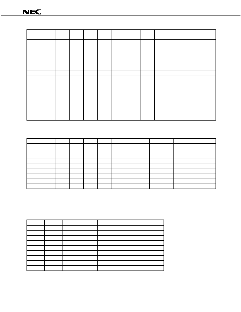
Preliminary Product Information S15797EJ1V4PM
26
µ
µ
µ
µ
PD161644
5.7 Division Ratio Selection of the DC/DC Converter OSC Frequency
LPM
FS0
FS1
FS2
FS3
LFS0
LFS1
LFS2
LFS3
Division ratio of the DC/DC converter
OSC frequency
0
0
0
x
x
x
x
x
x
V
DD2
, V
SS4
: f
OSC
/2
0
1
0
x
x
x
x
x
x
V
DD2
, V
SS4
: f
OSC
/4
0
0
1
x
x
x
x
x
x
V
DD2
, V
SS4
: f
OSC
/8
0
1
1
x
x
x
x
x
x
V
DD2
, V
SS4
: f
OSC
/16
0
x
x
0
0
x
x
x
x
V
DD1
, V
SS2
, V
SS3
: f
OSC
/2
0
x
x
1
0
x
x
x
x
V
DD1
, V
SS2
, V
SS3
: f
OSC
/4
0
x
x
0
1
x
x
x
x
V
DD1
, V
SS2
, V
SS3
: f
OSC
/8
0
x
x
1
1
x
x
x
x
V
DD1
, V
SS2
, V
SS3
: f
OSC
/16
1
x
x
x
x
0
0
x
x
V
DD2
, V
SS4
: f
OSC
/8
1
x
x
x
x
1
0
x
x
V
DD2
, V
SS4
: f
OSC
/16
1
x
x
x
x
0
1
x
x
V
DD2
, V
SS4
: f
OSC
/32
1
x
x
x
x
1
1
x
x
V
DD2
, V
SS4
: f
OSC
/64
1
x
x
x
x
x
x
0
0
V
DD1
, V
SS2
, V
SS3
: f
OSC
/8
1
x
x
x
x
x
x
0
0
V
DD1
, V
SS2
, V
SS3
: f
OSC
/16
1
x
x
x
x
x
x
1
1
V
DD1
, V
SS2
, V
SS3
: f
OSC
/32
1
x
x
x
x
x
x
1
1
V
DD1
, V
SS2
, V
SS3
: f
OSC
/64
Remark x: 0 or 1
5.8 Amp. Current Selection
RGON, RGONR
LPM
ACS0
ACS1
LACS0
LACS1
V
R
condition
V
S
condition
State of Circuit Current
0
x
x
x
x
x
V
SS1
V
SS1
Amp, CS Power OFF
1
0
0
0
x
x
Output
Output
Amp. current = 5
µ
A
1
0
0
1
x
x
Output
Output
Amp. current = 10
µ
A
1
0
1
0
x
x
Output
Output
Amp. current = 15
µ
A
1
0
1
1
x
x
Output
Output
Amp. current = 30
µ
A
1
1
x
x
0
0
Output
Output
Amp. current = 1.25
µ
A
1
1
x
x
0
1
Output
Output
Amp. current = 2.5
µ
A
1
1
x
x
1
0
Output
Output
Amp. current = 5
µ
A
1
1
x
x
1
1
Output
Output
Amp. current = 7.5
µ
A
Remark x: 0 or 1
5.9 V
R
Regulator Selection Output
Register control
RGONR
VRSEL0
VRSEL1
VRSEL2
V
R
0
x
x
x
V
R
regulator OFF (V
R
= V
SS1
)
1
0
0
0
3 V
: Internal resistor connection
1
1
0
0
3.5 V : Internal resistor connection
1
0
1
0
4 V
: Internal resistor connection
1
1
1
0
4.5 V : Internal resistor connection
1
0
0
1
4.75 V: Internal resistor connection
1
1
0
1
5 V
: Internal resistor connection
1
0
1
1
5.25 V: Internal resistor connection
1
1
1
1
5.5 V : Internal resistor connection
Remark x: 0 or 1

Preliminary Product Information S15797EJ1V4PM
27
µ
µ
µ
µ
PD161644
Pin control
RGONR
V
R
0
V
R
regulator OFF (V
R
= V
SS1
)
1
5 V: Internal resistor connection
5.10 V
S
Regulator Selection Output
Register control
RGON
EXRV
VSEL0
VSEL1
VSEL2
MVS condition
V
S
0
x
x
x
x
Hi-Z
V
S
regulator OFF (V
S
= V
SS1
)
1
1
x
x
x
Amp.-input
External resistor connection
1
0
0
0
0
Hi-Z
3 V
: Internal resistor connection
1
0
1
0
0
Hi-Z
3.5 V
: Internal resistor connection
1
0
0
1
0
Hi-Z
4 V
: Internal resistor connection
1
0
1
1
0
Hi-Z
4.5 V
: Internal resistor connection
1
0
0
0
1
Hi-Z
4.75 V : Internal resistor connection
1
0
1
0
1
Hi-Z
5 V
: Internal resistor connection
1
0
0
1
1
Hi-Z
5.25 V : Internal resistor connection
1
0
1
1
1
Hi-Z
5.5 V
: Internal resistor connection
Remark x: 0 or 1
Pin control
RGON
VSEL
V
R
0
x
V
S
regulator OFF (V
S
= V
SS1
)
1
0
5 V : Internal resistor connection
1
1
4 V : Internal resistor connection
Remark x: 0 or 1
5.11 Control of VM Output Control, VCOM Output
COMON
COMHI
DAC, COM_AMP
VCOM
0
x
OFF
Hi-Z
1
0
ON
Hi-Z
1
1
ON
Output
Remark x: 0 or 1
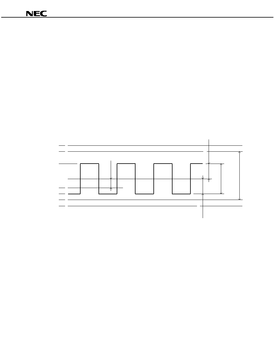
Preliminary Product Information S15797EJ1V4PM
28
µ
µ
µ
µ
PD161644
5.12 VCOM Output Frequency Adjustment
This is used to adjust the output amplitude of VCOM output. The VCOM output amplitude voltage (V
COMpp
) can be
adjusted as shown by the expression below using power supply control register 9 (R31), which is the output voltage of a
D/A converter circuit for which V
S
is the reference potential.
V
COMpp
= V
S
x 2 x {4/5 x (DA
R31
/255) }
Remark DA
R31
: R31 setting values
The values of R31 that can be set are determined by the relationship of booster voltages V
DD2
and V
SS4
to the potential
level of the actual common drive waveform after VCOM center adjustment.
Set the VCOM output amplitude voltage according to R31, the VCOM output center potential voltage setting level
according to power supply control register 10 (R32), or the VCOM output center potential input from VCOMIN in the
relationships shown in the figure below.
Figure 5-1. Voltage Ranges that can be set for Common Drive Waveform
V
DD2
V
DD2
-
0.2 V
VCOMC
V
SS4
+0.2 V
V
SS4
VCOMH
VCOML
COMpp
V
SS
1/2V
Voltage ranges that
can be set for common
drive waveform
COMpp
1/2V
COMpp
V
Common drive waveform
<Conditions on common drive waveform voltage settings>
V
COMpp
2 V
VCOMH
V
DD2
-
0.2 V
VCOML
V
SS4
+ 0.2 V
Remark VCOMH = 1/2 V
COMpp
+ VCOMC
VCOML = 1/2 V
COMpp
-
VCOMC
VCOMC: R32 setting values [COMSEL(R30) = 0] or VCOMIN input voltage level [COMSEL (R30) = 1]
5
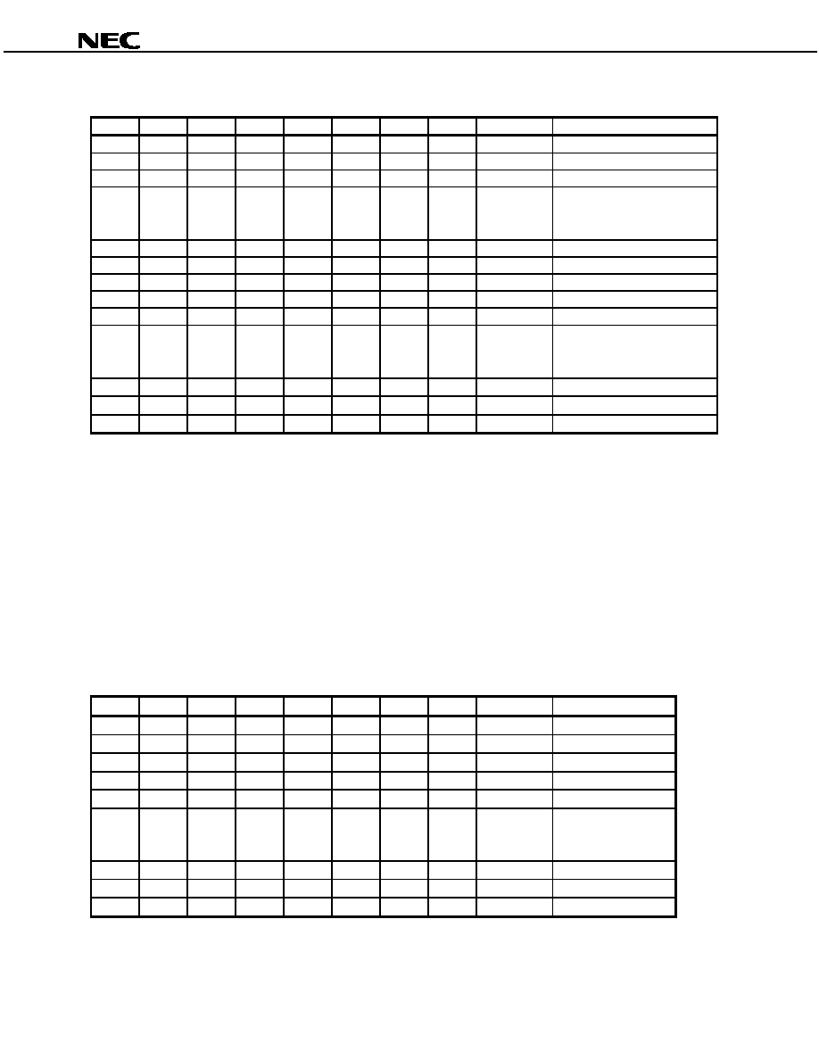
Preliminary Product Information S15797EJ1V4PM
29
µ
µ
µ
µ
PD161644
VCOM output amplitude voltage (V
COMpp
) adjustment and D/A converter setting values
DA
7
DA
6
DA
5
DA
4
DA
3
DA
2
DA
1
DA
0
DA
R31
V
COMpp
(V
S
= 5 V)
0
0
0
0
0
0
0
0
0
0.0000 V (Setting prohibited)
0
0
0
0
0
0
0
1
1
0.0314 V (Setting prohibited)
0
0
0
0
0
0
1
0
2
0.0627 V (Setting prohibited)
∑
∑
∑
∑
∑
∑
∑
∑
∑
∑
∑
∑
∑
∑
∑
∑
∑
∑
∑
∑
∑
∑
∑
∑
∑
∑
∑
∑
∑
∑
0
0
1
1
1
1
1
0
62
1.9451 V (Setting prohibited)
0
0
1
1
1
1
1
1
63
1.9765 V (Setting prohibited)
0
1
0
0
0
0
0
0
64
2.0078 V
0
1
0
0
0
0
0
1
65
2.0392 V
0
1
0
0
0
0
1
0
66
2.0706 V
∑
∑
∑
∑
∑
∑
∑
∑
∑
∑
∑
∑
∑
∑
∑
∑
∑
∑
∑
∑
∑
∑
∑
∑
∑
∑
∑
∑
∑
∑
1
1
1
1
1
1
0
1
253
7.9373 V
1
1
1
1
1
1
1
0
254
7.9686 V
1
1
1
1
1
1
1
1
255
8.0000 V
Remark The range in which the VCOM output amplitude can be varied is restricted by the output voltage of V
DD2
and
V
SS4
.
5.13 VCOM Output Center Adjustment
This is used to adjust the center potential level of VCOM output. The VCOM output center potential voltage (V
COMC
)
can be adjusted as shown by the expression below using power supply control register 9 (R32), which is the output
voltage of a D/A converter circuit for which V
S
is the reference potential.
V
COMpp
= V
S
x {4/5 x (DA
R32
/255) }
Remark DA
R32
: R32 setting values
VCOM output center potential voltage (V
COMC
) and D/A converter setting values
DA
7
DA
6
DA
5
DA
4
DA
3
DA
2
DA
1
DA
0
DA
R31
V
COMC
(V
S
= 5 V)
0
0
0
0
0
0
0
0
0
0.0000 V
0
0
0
0
0
0
0
1
1
0.0157 V
0
0
0
0
0
0
1
0
2
0.0314 V
0
0
0
0
0
0
1
1
3
0.0471 V
0
0
0
0
0
1
0
0
4
0.0627 V
∑
∑
∑
∑
∑
∑
∑
∑
∑
∑
∑
∑
∑
∑
∑
∑
∑
∑
∑
∑
∑
∑
∑
∑
∑
∑
∑
∑
∑
∑
1
1
1
1
1
1
0
1
253
3.9686 V
1
1
1
1
1
1
1
0
254
3.9843 V
1
1
1
1
1
1
1
1
255
4.0000 V
Remark The range in which the VCOM output center can be varied is restricted by the output voltage of V
DD2
and V
SS4
.
5
Preliminary Product Information S15797EJ1V4PM
30
µ
µ
µ
µ
PD161644
The values of R32 that can be set are determined by the relationship of booster voltages V
DD2
and V
SS4
to the potential
level of the actual common drive waveform due to VCOM output amplitude voltage (V
COMpp
) adjustment.
Refer to 5.12 VCOM Output Frequency Adjustment for the relationship between the VCOM output center potential
voltage according to R32 and the VCOM output amplitude voltage (V
COMpp
) according to power supply control register 9
(R31).
5.14 VCOM Center Adjustment Selection
The method of setting the center voltage of common drive waveform VCOM is selected according to the setting of
COMSEL (R30).
When COMSEL is set to 1, directly input the VCOM center voltage to the VOMIN pin from outside the IC.
COMSEL
VCOM center adjustment
0
Internal D/A is valid (R31 setting is valid).
1
VCOMIN input voltage is valid.
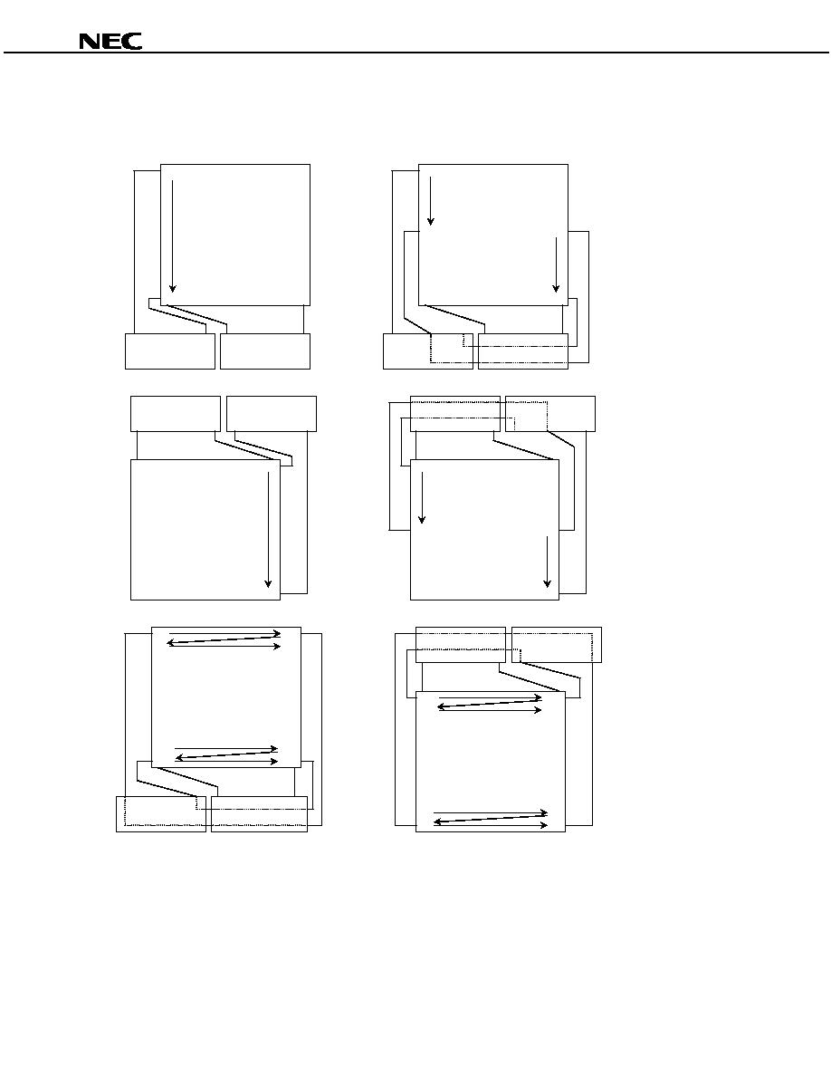
Preliminary Product Information S15797EJ1V4PM
31
µ
µ
µ
µ
PD161644
6. PANNEL CONNECTION EXAMPLES
[MODE1]
TFT
Panel
µ
PD161644
Source driver
1
240
1
240
MODE1R (SCN0 = 1, SCN1 = 1, SCN2 = 1, R,/L = 1)
TFT
Panel
240
µ
PD161644
Source driver
1
1
240
MODE1R (SCN0 = 1, SCN1 = 1, SCN2 = 1, R,/L = 1)
121
122
1
TFT
Panel
Source driver
µ
PD161644
2
241
2
241
MODE1L (SCN0 = 1, SCN1 = 1, SCN2 = 1, R,/L = 0)
TFT
Panel
Source driver
MODE1L (SCN0 = 1, SCN1 = 1, SCN2 = 1, R,/L = 0)
241
µ
PD161644
2
122,121
2
241
122
121
TFT
Panel
240
µ
PD161644
Source driver
1
1
239
MODE1R (SCN0 = 1, SCN1 = 1, SCN2 = 1, R,/L = 1)
240
2
3
4
237
238
µ
PD161644
TFT
Panel
Source driver
MODE1L (SCN0 = 1, SCN1 = 1, SCN2 = 1, R,/L = 0)
241
2
2
241
3
4
239
240
238
5
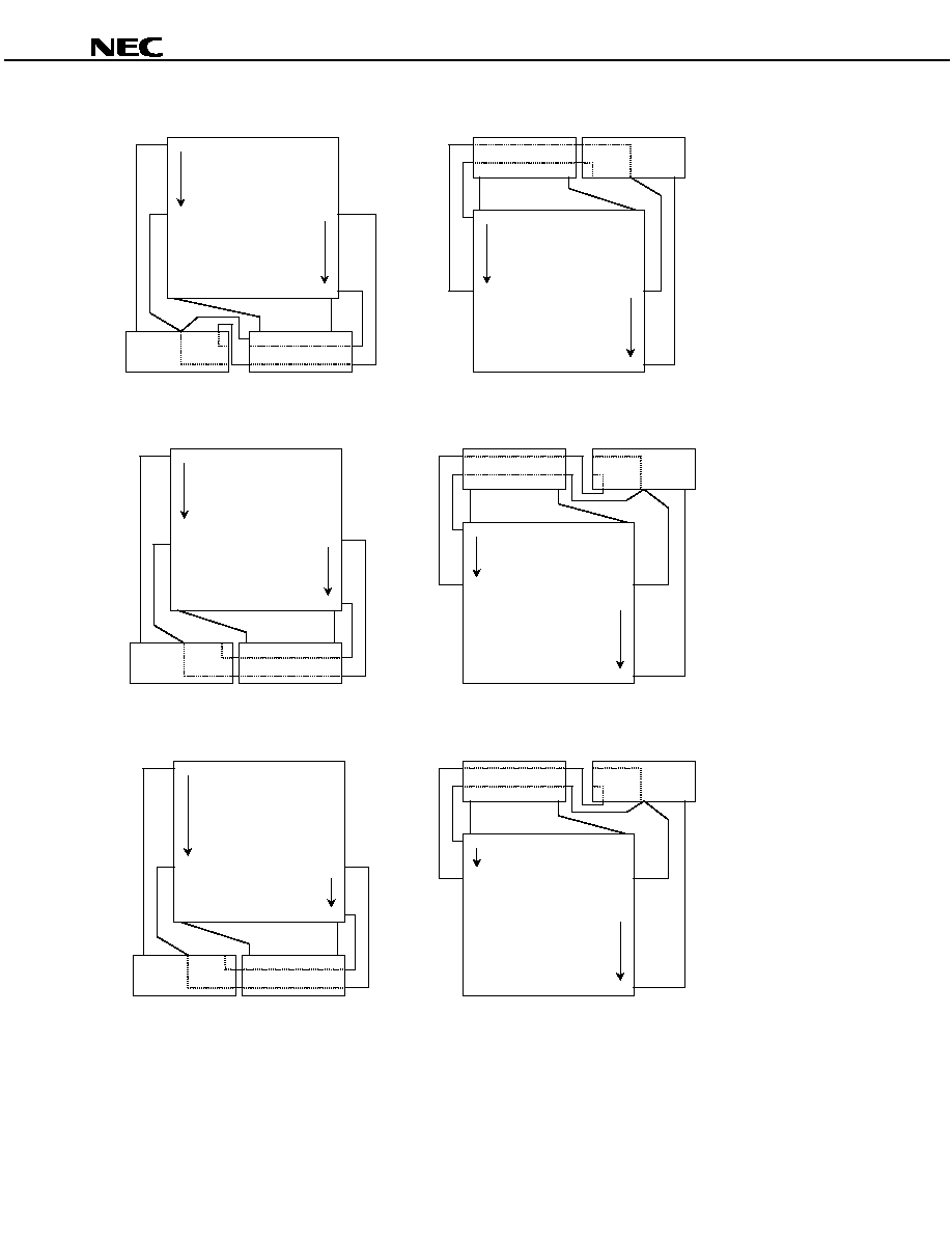
Preliminary Product Information S15797EJ1V4PM
32
µ
µ
µ
µ
PD161644
[MODE2]
TFT
Panel
241
µ
PD161644
Source driver
1
1
123
MODE2R (SCN0 = 1, SCN1 = 1, SCN2 = 0, R,/L = 1)
121
241
121,123
TFT
Panel
Source driver
MODE2L (SCN0 = 1, SCN1 = 1, SCN2 = 0, R,/L = 0)
241
µ
PD161644
2
122,121
2
122
241
121
[MODE3]
TFT
Panel
241
µ
PD161644
Source driver
1
1
163
MODE3R (SCN0 = 1, SCN1 = 0, SCN2 = 1, R,/L = 1)
161
241
161,163
TFT
Panel
Source driver
MODE3L (SCN0 = 1, SCN1 = 0, SCN2 = 1, R,/L = 0)
241
µ
PD161644
2
162,161
2
162
241
161
[MODE4]
TFT
Panel
241
µ
PD161644
Source driver
1
1
203
MODE4R (SCN0 = 1, SCN1 = 0, SCN2 = 0, R,/L = 1)
201
241
201,203
TFT
Panel
Source driver
MODE4L (SCN0 = 1, SCN1 = 0, SCN2 = 0, R,/L = 0)
241
µ
PD161644
2
202,201
2
202
241
201
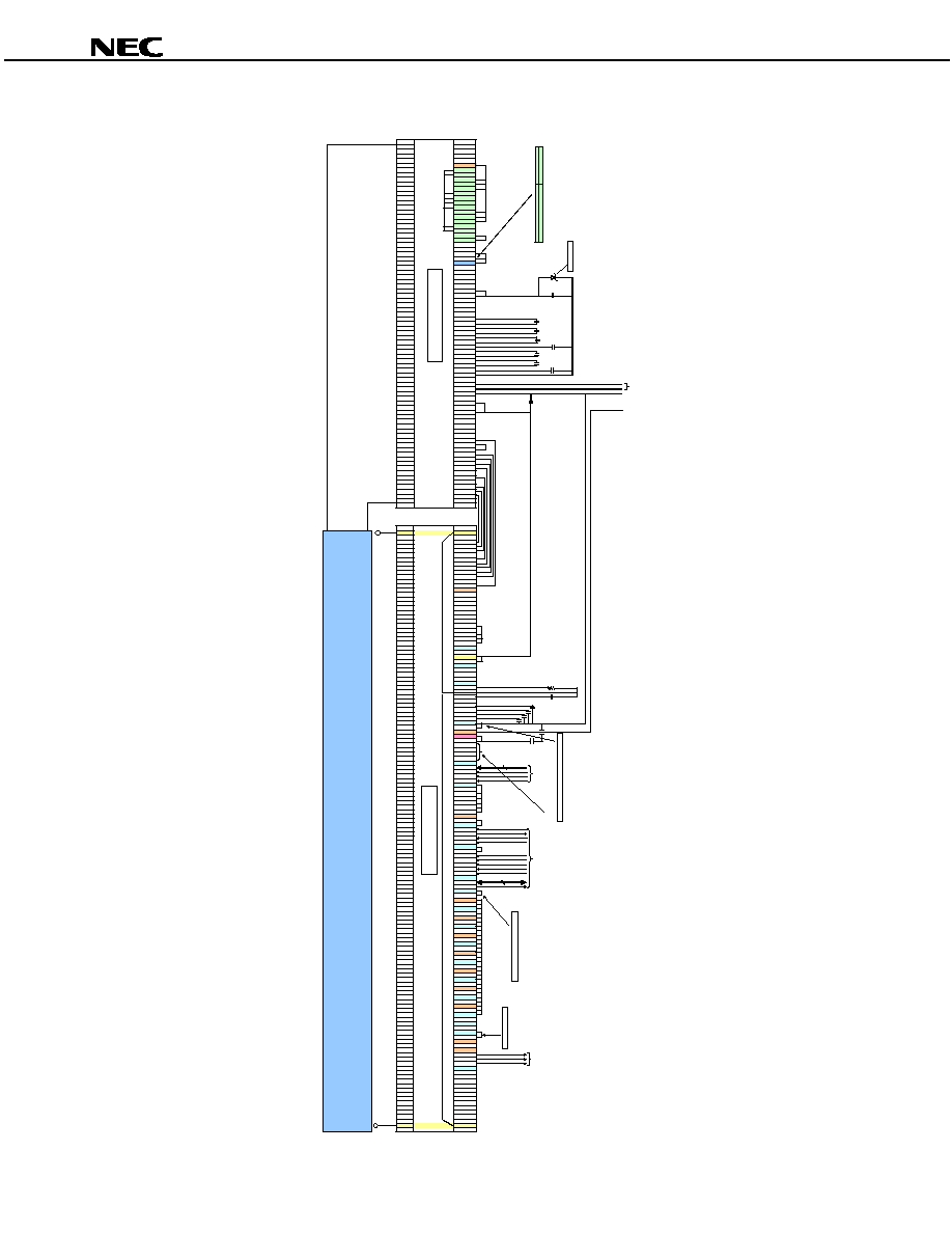
Preliminary Product Information S15797EJ1V4PM
33
µ
µ
µ
µ
PD161644
7. CONNECTION EXAMPLE WITH SOURCE DRIVER
DUMMY
VC1
DUMMY
Y1
Y2
Y3
DUMMY
VC1
DUMMY
GFRM
VCOUT3
/GRESET
GCS
GCL
GDA
GSTB
DMSTB
GCLK
GOE1
GOE2
VSS(MODE)
/BLCS_O
BLSCL
BLSDA
VCC1(MODE)
TOUT0-17
VCC1(MODE)
OSCSEL
VSS(MODE)
OSCOUT
VSS(MODE)
OSCIN
VSS(MODE)
SCLEG1
VCC1(MODE)
SCLEG0
VSS(MODE)
HSEG
VCC1(MODE)
VSEG
VSS(MODE)
DCKEG
VCC1(MODE)
PSX
VSS(MODE)
C86
VCC1(MODE)
DTX1
VSS(MODE)
DTX2
VCC1(MODE)
BWS0
VSS(MODE)
BWS1
VCC1(MODE)
BWS2
VSS(MODE)
DDS
VCC1(MODE)
IF_SHARE
VSS(MODE)
CSTB
D0-D17
VSS(MODE)
/CS
/RESET
RS
/WR
/RD
RGB/CPU
VSS(MODE)
SI
BU
MP SIDE UP
CPU interface
Y526
Y527
SCL
SO
BLCS_I
VSS(MODE)
TDELAY1-6
VCC1(MODE)
TSTVIHL
TSTRTST
TOSCSELO
TOSCSELI
TOSCI
TOSCO
VSS(MODE)
VSYNC
HSYNC
DOTCLK
RGB00-25
VSS(MODE)
VCD2
LPM
RGON
DCON
SF_VCC1
VCC11
VCC1
VSTBY
VSS
CVNL
CVNH
CVPL
CVPH
DUMMY
VCOUT1
DUMMY
VCOM
DUMMY
VSS(MODE)
VCOMR
BGRIN
VSS(MODE)
FBRSEL
VS
V0-V5
VCOUT2
VSS(MODE)
TBSEL1
TBSEL2
TBGR
DAC0-DAC7
DUMMY
TOUT
DUMMY
TOUT
TOUT
TOUT
TOUT
VCC1
GFRM
VCOUT3
/GRESET
GCS
GCL
GDA
GSTB(STV)
DMSTB
GCLK(CPV)
GOE1
Because of using specified interface for gate driver interface,
leave them open.
Y528
DUMMY
VC2
DUMMY
DUMMY
O241
O240
GOE2
DUMMY
VC2
DUMMY
DUMMY
VSS3
OE2
OE1
CLK
DCCLK
STVL
STVR
GDA
GCL
GCS
/GRESET
PVSS1
VCIN
FRM
DCON
RGON
VCD2
PVCC1
DUMMY
VS
MVS
VGD
VR
VSS1
VCC1
VDC
DUMMY
VSS1
VDD2
C1+
C1-
C2+
C2-
VDD1
C3+
C3-
C4+
C4-
C5+
C5-
C6+
C6-
VSS2
VSS4
VSS3
VB
VM
COMH
COML
VCOM
VCOMIN
PVSS1
IFSEL
R,/L
PVCC1
BUMP SIDE UP
1 uF/25 V
Schottky diode
DUMMY
VMON
PVSS3
PVSS1
RGONR
VMS
FS0
FS2
CLS0
VSEL
EXRV
ACS0
SCN0
SCN1
SCN2
PUPT0
DUPF0
PVCC1
TESTOUT1
TESTIN1
TESTIN2
TESTOUT2
DUMMY
IFSEL : L (when in serial interface input)
OPEN (pull-down)
IFSEL : H (control pin input)
Connect to PVSS/PVCC1
2.5 to 3.3 V
VSS
VC
C
+
DUMMY
Generate logic part supply voltage inside
µ
PD161621.
2.5 to 3.3 V
0.1 uF/10 V
0.1 uF/10 V
0.1 uF/10 V
1 uF/25 V
1 uF/10 V
1 uF/10 V
1 uF/10 V
Using D17-D01 only as parallel interface.
Select on-chip oscillator
Back panel LCD control
RGB interface
O2
O1

Preliminary Product Information S15797EJ1V4PM
34
µ
µ
µ
µ
PD161644
8. VALUE OF WIRING RESISTANCE TO EACH PIN
The recommended wiring resistance values are shown below. The wiring resistance values affect the current capacity
of the power supply, so be sure to design using values that do not exceed those recommended.
Table 8-1. Recommended Wiring Resistor Values
Pin name
Wiring Resistor Values (
)
V
SS1
< 10
V
CC1
< 10
V
DC
< 10
V
S
< 10
V
DD2
< 10
C
1
+
< 10
C
1
-
< 10
C
2
+
< 10
C
2
-
< 10
V
DD1
< 50
V
SS2
< 50
V
SS3
< 50
V
SS4
< 50
C
3
+
< 50
C
3
-
< 50
C
4
+
< 50
C
4
-
< 50
C
5
+
< 50
C
5
-
< 50
C
6
+
< 50
C
6
-
< 50
Preliminary Product Information S15797EJ1V4PM
35
µ
µ
µ
µ
PD161644
9. RECOMMENDED CAPACITANCE VALUES OF EXTERNAL CAPACITOR
The recommended capacitance values of the external capacitor are shown below. These values should be finally
determined only after performing sufficient evaluation on the module.
Table 9-1. Recommended Values of External Capacitor
Pin name
Recommended value of
capacitors (
µ
F)
Withstanding voltage (V)
V
S
1 to 4.7
6.3 or more
V
R
1 to 4.7
6.3 or more
V
DD1
0.47 to 1
25 or more
V
DD2
1 to 4.7
15 or more
V
SS2
0.47 to 1
25 or more
V
SS3
0.47 to 1
25 or more
V
SS4
1 to 4.7
10 or more
COMH
1 to 4.7
6.3 or more
COML
1 to 4.7
6.3 or more
C
1
+
, C
1
-
1 to 4.7
10 or more
C
2
+
, C
1
-
1 to 4.7
10 or more
C
3
+
, C
1
-
0.47 to 1
10 or more
C
4
+
, C
1
-
0.47 to 1
10 or more
C
5
+
, C
1
-
0.47 to 1
10 or more
C
6
+
, C
1
-
1 to 4.7
10 or more

Preliminary Product Information S15797EJ1V4PM
36
µ
µ
µ
µ
PD161644
10. SERIAL INTERFACE
When the serial interface has been selected, if the chip is active (GCS = L), serial data input (GDA) and serial clock
input (GCL) can be received. Serial data is read from D
7
and then from D
6
to D
0
on the rising edge of the serial clock, via
the serial input pin. This data is synchronized on the eighth serial clock's rising edge and is then converted to parallel
data for processing.
The serial interface signal chart is shown below.
Figure 10-1. Serial Interface Signal Chart
GCL
Command
GCS
GDA
A
7
A
6
A
5
A
4
A
3
A
2
A
1
A
0
D
7
D
6
D
5
D
4
D
3
D
2
D
1
D
0
1
2
3
4
5
6
7
8
9
10
11
12
13
14
15
16
Data to set command
Note that odd bytes of data received after the reset command is input are recognized as commands, and even bytes
of data are recognized as data values to be set to commands.
Remarks 1. The shift register and counter are reset to their initial values when the chip select signal is inactive. Do not
set the chip select signal to inactive between transmission of an 8-bit command and transmission of the 8-
bit data set for the command.
2. When using GCL wiring, take care concerning the possible effects of terminating reflection and noise from
external sources. We recommend checking operation with the actual device.
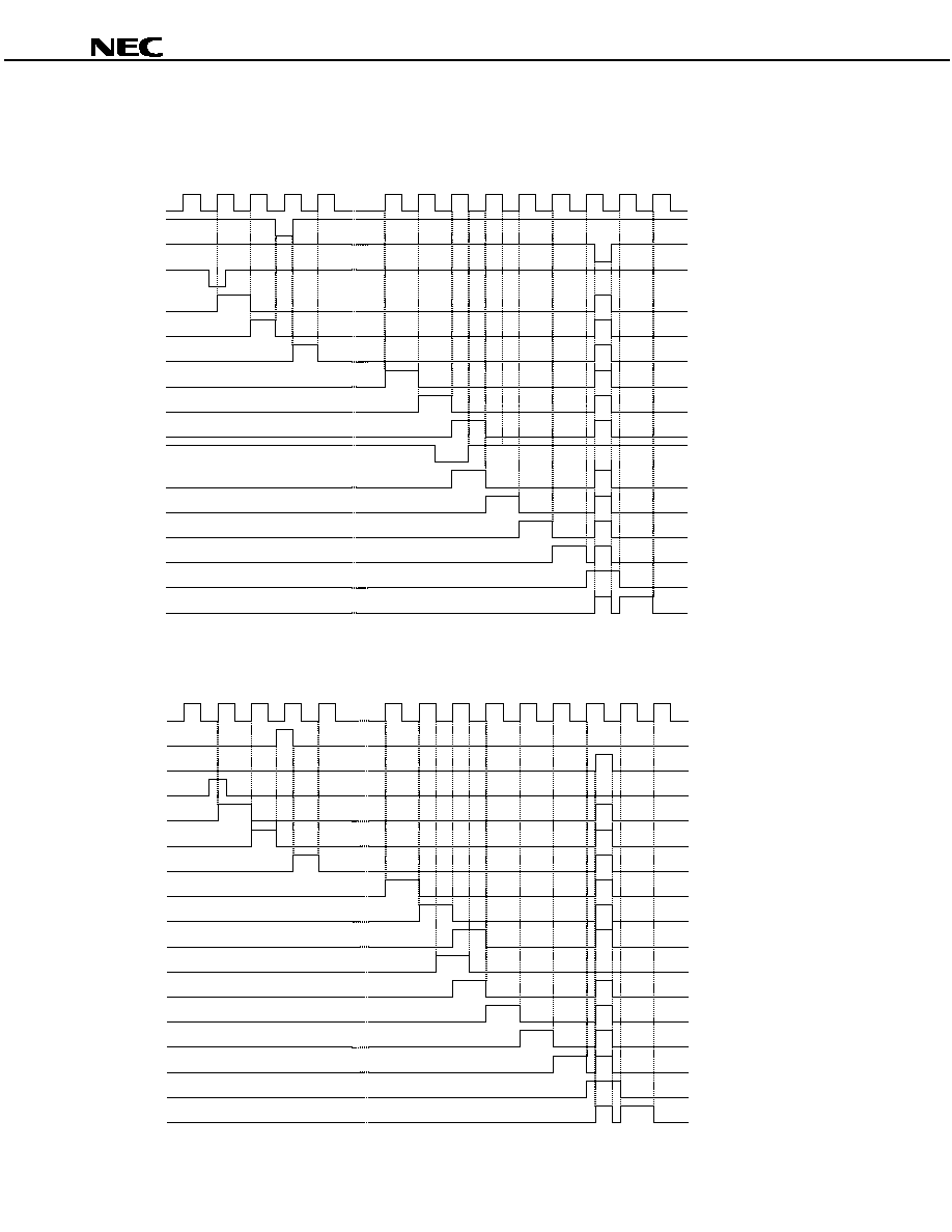
Preliminary Product Information S15797EJ1V4PM
37
µ
µ
µ
µ
PD161644
11. TIMING CHARTS (MODE1: SCN0 = 1, SCN1 = 1, SCN2 = 1)
R,/L = H, STVSEL = 0, OE1SEL = 0, OE2SEL = 0
CLK
OE
1
STVR
STVL
O
241
O
240
O
239
O
3
O
2
O
1
1
2
3
4
239 240 241 242 243 244 245 246 247
OE
2
(O
1
)
(O
2
)
(O
3
)
(O
4
)
(O
5
)
(O
6
)
R,/L = L, STVSEL = 1, OE1SEL = 1, OE2SEL = 1
CLK
OE
1
STVL
STVR
O
241
O
1
O
2
O
238
O
239
O
240
1
2
3
4
239 240 241 242 243 244 245 246 247
OE
2
(O
240
)
(O
239
)
(O
238
)
(O
237
)
(O
236
)
(O
235
)

Preliminary Product Information S15797EJ1V4PM
38
µ
µ
µ
µ
PD161644
12. POWER ON/OFF SEQUENCE
There are three ways to turn on the power of the
µ
PD161644:
<When power supply is controlled by serial interface>
∑
Simple sequence
∑
Command control sequence
<When power supply is controlled by pin>
∑
Simple sequence
12.1 Power ON sequence
(1) Power supply control via serial interface (simple sequence)
Control /GRESET pin and each command of PONM, VD2ON, RGONR, RGON, VS2ON, VS3ON, VD1ON, and DCON
using the following sequence, after applying power to V
DC
, V
CC1
, and V
CC11
.
V
DC
V
CC1
V
CC11
0 ns MIN.
2.5 V
1.8 V
/GRESET
PONM
Wait
0 ns MIN.
Power-on operation is complete after the
time specified by PUPT0 and PUPT1 has
elapsed.
DCON
<1> Issue the reset command (R34)
<2> Set a value to R25 to R33 (any value)
0 ns MIN.
Wait
0 ns MIN.
Wait
0 ns MIN.
Turn on the power
supply to be used
Note
Note Turn on the power supply to be used among VD2ON, RGONR, RGON, VS2ON, VS3ON, and VD1ON.
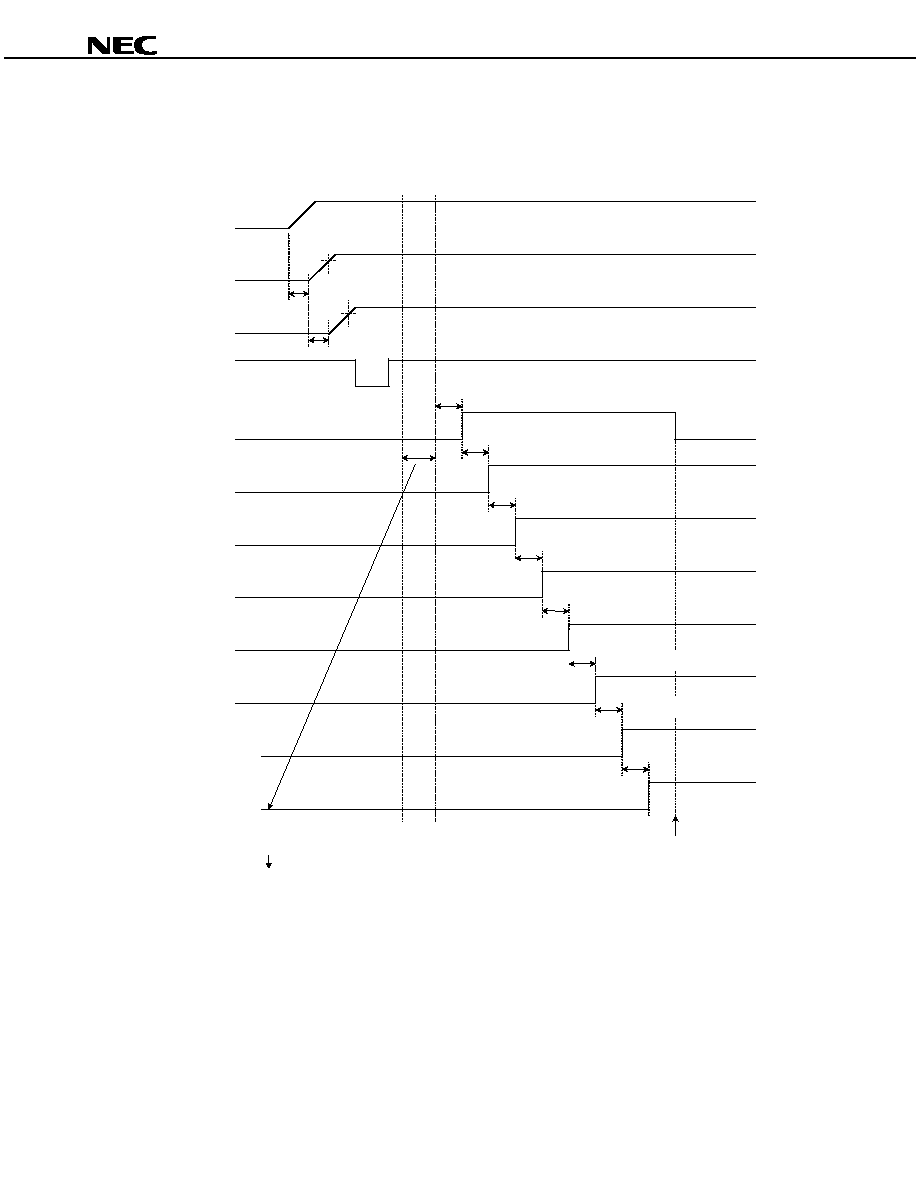
Preliminary Product Information S15797EJ1V4PM
39
µ
µ
µ
µ
PD161644
(2) Power control by serial interface (command control sequence)
Control /GRESET pin and each command of PON, DCON, VD2ON, RGONR, RGON, VS2ON, VS3ON, VD1ON, and
VS4ON after power on of V
DC
, V
CC1
, V
CC11
as shown below.
V
DC
V
CC1
V
CC11
0 ns MIN.
2.5 V
1.8 V
/GRESET
PON
Wait
0 ms
MIN.
Power-on operation is complete.
DCON
<1> Issue the reset command (R34)
<2> Set a value to R25 to R32 (any value)
0 ns MIN.
Wait
0 ms
MIN.
Wait
1 ms
MIN.
VD2ON
RGONR
NOTE 1
VD1ON
VS4ON
NOTE 3
VS2ON, VS3ON
NOTE 2
RGON
Wait
0 ms
MIN.
Wait 4
0 ms
MIN.
Wait 6
0 ms
MIN.
Wait 6
0 ms
MIN.
Wait 6
0 ms
MIN.
Wait 25
ms
MIN.
Notes 1. This pin only needs to be controlled when the V
R
amplifier is used.
2. VS2ON only needs to be controlled when V
SS2
is used.
3. This pin only needs to be controlled when VCOM is used.
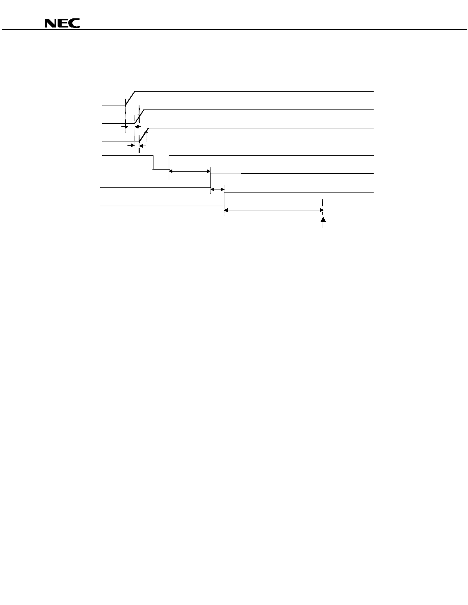
Preliminary Product Information S15797EJ1V4PM
40
µ
µ
µ
µ
PD161644
(3) Power control by pins (simple sequence)
Control each pin of /GRESET, RGON, and DCON after power on of V
DC
, V
CC1
, V
CC11
as shown below.
V
DC
V
CC1
V
CC11
/GRESET
RGON
wait 0 ms MIN.
DCON
0 ns MIN.
0 ns MIN.
2.5 V
1.8 V
Power supply startup is complete after the time
specified by PUPT0 and PUPT1 has elapsed
wait 10 ms MIN.
Remarks 1. When using RGON, pull it up to the high level by wiring the RGONR pin.
2. When using V
SS4
, pull it up to the high level by wiring the COMON pin.
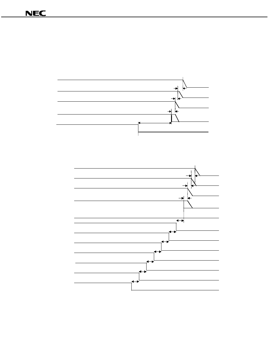
Preliminary Product Information S15797EJ1V4PM
41
µ
µ
µ
µ
PD161644
12.2 Power OFF sequence
When turning the power off, turn off the pins and commands used for control simultaneously, both when performing
control via the serial interface and via the pins.
(1) Power control by serial interface (Simplified sequence)
Control DCON pin as shown below.
DCON
V
DC
V
CC1
V
CC11
0 ns
0 ns
0 ns
/GRESET
0 ns
(2) Power control by serial interface (Command control sequence)
Control each pin of /GRESET, RGON, and DCON as shown below.
DCON
RGON
VS2ON, VS3ON
Note2
VD2ON
0 ms
0 ms
RGONR
Note3
0 ms
VD1ON
VS4ON
Note1
0 ms
0 ms
0 ms
PON
0 ms
V
DC
V
CC1
V
CC11
0 ns
0 ns
0 ns
/GRESET
Notes 1. This pin only needs to be controlled when the VCOM is used.
2. VS2ON only needs to be controlled when V
SS2
is used.
3. This pin only needs to be controlled when V
R
amplifier is used.
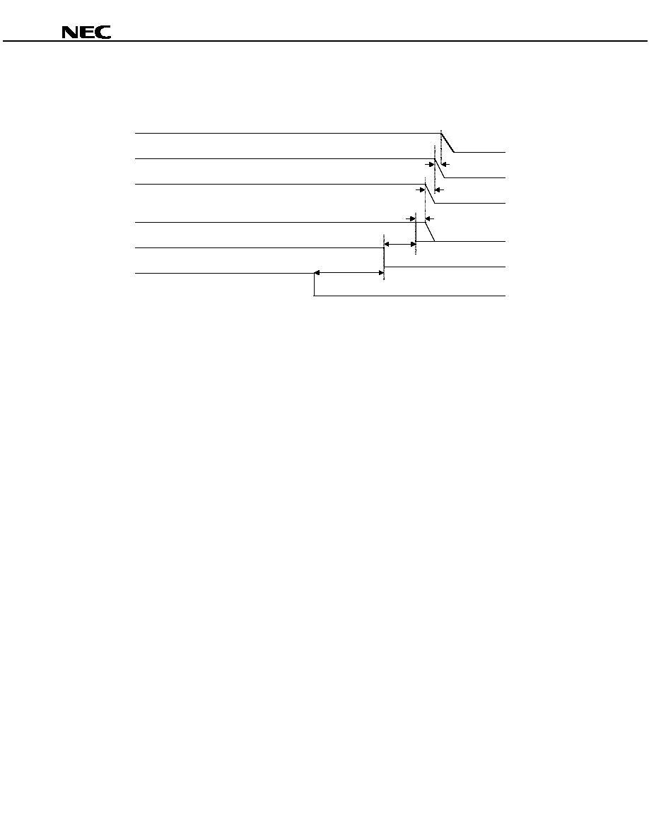
Preliminary Product Information S15797EJ1V4PM
42
µ
µ
µ
µ
PD161644
(3) Power control by pins (Simplified sequence)
Control each pin of /GRESET, RGON, and DCON as shown below.
V
DC
V
CC1
V
CC11
/GRESET
RGON
DCON
0 ns
0 ns
0 ns
0 ns
0 ns
Remarks 1. When using RGON, pull it up to the high level by wiring the RGONR pin.
2. When using V
SS4
, pull it up to the high level by wiring the COMON pin.

Preliminary Product Information S15797EJ1V4PM
43
µ
µ
µ
µ
PD161644
13. ELECTRICAL SPECIFICATIONS
Absolute Maximum Ratings (T
A
= 25
∞
∞
∞
∞
C, V
SS
= 0 V)
Parameter
Symbol
Rating
Unit
Supply Voltage
V
CC1
-
0.5 to +4.0
V
Supply Voltage
V
DC
-
0.5 to +4.0
V
Supply Voltage
V
SS3
V
DD1
-
42 V to +0.5
V
Supply Voltage
V
DD1
-V
SS3
-
0.5 to +42
V
Input Voltage
Note 1
V
I
-
0.5 to V
CC1
+0.5
V
Input Current
Note 1
I
I
±
1
mA
Output Current
Note 2
I
O1
±
10
mA
Output Current
Note 3
I
O2
+10
mA
Operating Ambient Temperature
T
A
-
40 to +85
∞
C
Storage Temperature
T
stg
-
55 to +150
∞
C
Notes 1. CLK, STVR, STVL, R,/L, OE
1
, OE
2
, GCS, GCL, GDA, DCCLK, VCIN, DCON, RGON, VCD2, /GRESET,
IFSEL, EXRV, SCN0, SCN1
2. STVR, STVL, VM, VCOM
3. V
S
Caution Product quality may suffer if the absolute maximum rating is exceeded even momentarily for any
parameter. That is, the absolute maximum ratings are rated values at which the product is on the
verge of suffering physical damage, and therefore the product must be used under conditions that
ensure that the absolute maximum ratings are not exceeded.
Recommended Operating Conditions (T
A
= ≠40 to +85
∞
∞
∞
∞
C, V
SS
= 0 V)
Parameter
Symbol
Condition
MIN.
TYP.
MAX.
Unit
Supply Voltage
V
CC1
2.5
2.7
3.3
V
Supply Voltage
V
DC
2.5
2.7
3.3
V
Supply Voltage
V
DD1
10
15
20
V
Supply Voltage
V
SS3
-
20
-
15
-
10
V
Supply Voltage
V
DD1
-V
SS3
20
30
40
V
Supply Voltage
V
GD
6.0
V
Input Voltage
Note
V
I
0
V
CC1
V
Note CLK, STVR, STVL, R,/L, OE
1
, OE
2
, GCS, GCL, GDA, DCCLK, VCIN, DCON, RGON, VCD2, /GRESET, IFSEL,
EXRV, SCN0, SCN1
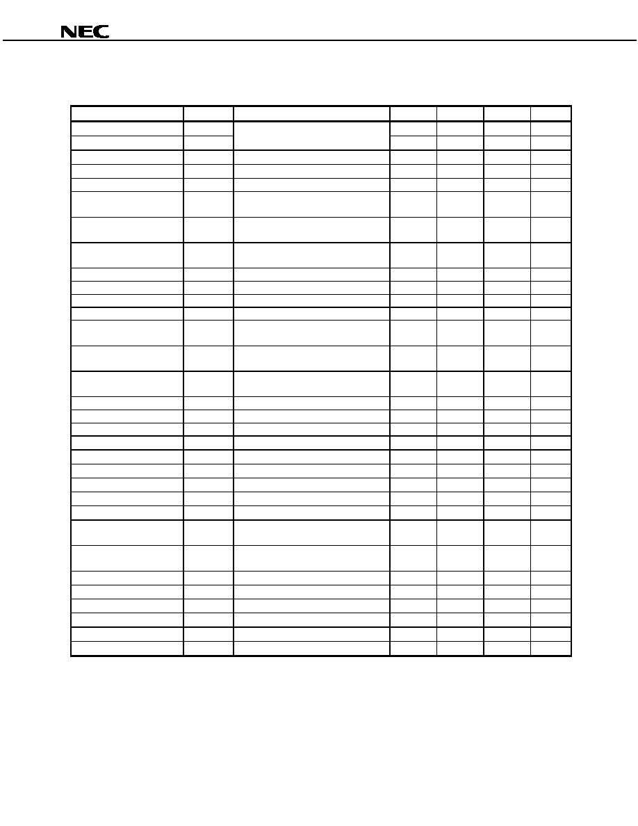
Preliminary Product Information S15797EJ1V4PM
44
µ
µ
µ
µ
PD161644
Electrical Characteristics (T
A
=
-
-
-
-
40 to +85
∞
∞
∞
∞
C, V
CC1
= 2.5 to 3.3 V, V
DC
= 2.5 to 3.3 V, V
DD1
= 15 V, V
SS3
=
-
-
-
-
15 V,
V
S
= 5 V, V
SS1
= 0 V)
(1/2)
Parameter
Symbol
Condition
MIN.
TYP.
MAX.
Unit
High-level input voltage
V
IH1
0.8 V
CC1
V
Low-level input voltage
V
IL1
Note 1
0.2 V
CC1
V
High-level output voltage
V
OH
STVR, STVL, I
OH
=
-
40
µ
A
V
CC1
-
0.4
V
CC1
V
Low-level output voltage
V
OL
STVR, STVL, I
OH
= +40
µ
A
0
0.4
V
V
DD1
boost voltage
V
DD1
I
DD1
= 300
µ
A, 3 x boost, Note 2
2.7 V
GD
-
3 V
GD
V
V
DD2
boost voltage1
V
DD21
I
DD2
= 1 mA , V
CD2
= L, V
MS
= H (2 x
boost, dual), Note 2
1.9 V
DC
-
2 V
DC
V
V
DD2
boost voltage2
V
DD22
I
DD2
= 1 mA , V
CD2
= L, V
MS
= L (2 x
boost, single), Note 2
1.8 V
DC
-
2 V
DC
V
V
DD2
boost voltage3
V
DD23
I
DD2
= 1 mA , V
CD2
= H (3 x boost),
Note 2
2.7 V
DC
-
3 V
DC
V
V
SS2
boost voltage
V
SS2
I
SS2
=
-
300
µ
A,
-
2 x boost, Note 2
-
2 V
S
-
-
1.8 V
S
V
V
SS3
boost voltage
V
SS3
I
SS3
=
-
300
µ
A,
-
3 x boost, Note 2
-
3 V
S
-
-
2.7 V
S
V
V
SS4
boost voltage
V
SS4
I
SS4
=
-
300
µ
A,
-
1 x boost, Note 2
-
V
DC
-
-
0.9 V
DC
V
V
DD1
output resister
R
VDD1
I
DD1
= 300
µ
A, 3 x boost, Note 2
-
3
5
k
V
DD2
output resistor1
R
VDD21
I
DD2
= 1 mA , V
CD2
= L, V
MS
= H (2x
boost, dual), Note 2
-
100
200
V
DD2
output resistor2
R
VDD22
I
DD2
= 1 mA , V
CD2
= L, V
MS
= L (2x
boost, single), Note 2
-
250
400
V
DD2
output resistor3
R
VDD23
I
DD2
= 1 mA , V
CD2
= H (3 x boost),
Note 2
-
450
700
V
SS2
output resistor
R
VSS2
I
SS2
=
-
300
µ
A ,
-
2 x boost, Note 2
-
3
5
k
V
SS3
output resistor
R
VSS3
I
SS2
=
-
300
µ
A ,
-
3 x boost, Note 2
-
3
5
k
V
SS4
output resistor
R
VSS4
I
SS2
=
-
300
µ
A ,
-
1 x boost, Note 2
-
300
500
V
S
output voltage
V
S
No load
4.5
5
5.5
V
V
R
output voltage
V
R
No load
4.5
5
5.5
V
V
S
output resistor
R
VS
V
DD2
= 6 V, I
S
= 1 mA, V
S
= 5 V
-
15
30
V
R
output resistor
R
VR
V
DD2
= 6 V, I
R
= 1 mA, V
R
= 5 V
-
15
30
COMH output voltage
V
comH
No load, DA (7:0) = CDA (7:0) = A0H
4.5
5
5.5
V
COML output voltage
V
comL
No load, DA (7:0) = CDA (7:0) = A0H
-
0.5
0
0.5
V
VCOM output high-level
voltage
V
VcomH
I
VCOM
= 1 mA, DA (7:0) = CDA (7:0) =
A0H, VCIN = H
4.5
5
5.5
V
VCOM output low-level
voltage
V
VcomL
I
VCOM
=
-
1 mA, DA (7:0) = CDA (7:0) =
A0H, VCIN = L
-
0.5
0
0.5
V
COM output resistor1
R
COM1
COM output = High, I
COM
= 1 mA
-
100
200
COM output resistor2
R
COM2
COM output = Low, I
COM
=
-
1 mA
-
100
200
VM output high-level voltage V
M1H
No load
0.9 V
SS2
V
SS2
1.1 V
SS2
V
VM output low-level voltage
V
M1L
No load
0.9 V
SS3
V
SS3
1.1 V
SS3
V
VM output resistance
R
M1
When I
VM
= 100
µ
A, V
SS2
is selected.
-
300
400
Output ON resistance
R
ON1
O
1
to O
241
1
2
4
k
Notes 1. CLK, STVR, STVL, R,/L, OE
1
, OE
2
, GCS, GCL, GDA, VCOM, DCON, RGON, LPM, VCD2, /GRESET, IFSEL,
EXRV, SCN0, SCN1, VCIN
2. External capacitor: 1
µ
F, CLS0 = H, CLS1 = L, FS0 = H, FS1 = L, FS2 = H, FS3 = L, FUP = L
3. ACS0 = H, ACS1 = H, V
DD2
= V
DC
x 2, dual mode, V
DD1
= VGD x 3, V
SS2
= VGD x (
-
2), V
SS3
= VGD x (
-
3),
V
SS4
= V
DC
x (
-
1), VGD = V
S
, CLS0 = H, CLS1 = L, FS0 = H, FS1 = L, FS2 = H, FS3 = L, FUP = L

Preliminary Product Information S15797EJ1V4PM
45
µ
µ
µ
µ
PD161644
(2/2)
Parameter
Symbol
Condition
MIN.
TYP.
MAX.
Unit
Input current
I
I1
Note 1
≠
1
0
1
µ
A
Input leak current
I
IL
STVR, STVL
≠
1
0
1
µ
A
Dynamic current
I
CC1
V
CC1
, f
CLK
= 12.5 kHz, no load, Note 3
-
-
200
µ
A
Dynamic current
I
DC
V
DC
, f
CLK
= 12.5 kHz, no load, Note 3
-
-
1.8
mA
Static current
I
CC1
V
CC1
, stand-by
-
-
5
µ
A
Static current
I
DC
V
DC
, stand-by
-
-
5
µ
A
V
REF
voltage
V
REF
1.08
1.20
1.32
V
Notes 1. CLK, STVR, STVL, R,/L, OE
1
, OE
2
, GCS, GCL, GDA, VCOM, DCON, RGON, LPM, VCD2, /GRESET, IFSEL,
EXRV, SCN0, SCN1, VCIN
2. External capacitor: 1
µ
F, CLS0 = H, CLS1 = L, FS0 = H, FS1 = L, FS2 = H, FS3 = L, FUP = L
3. ACS0 = H, ACS1 = H, V
DD2
= V
DC
x 2, dual mode, V
DD1
= VGD x 3, V
SS2
= VGD x (
-
2), V
SS3
= VGD x (
-
3),
V
SS4
= V
DC
x (
-
1), VGD = V
S
, CLS0 = H, CLS1 = L, FS0 = H, FS1 = L, FS2 = H, FS3 = L, FUP = L

Preliminary Product Information S15797EJ1V4PM
46
µ
µ
µ
µ
PD161644
Switching Characteristics (T
A
=
-
40 to +85
∞
∞
∞
∞
C, V
CC1
= 2.5 to 3.3 V, V
DC
= 2.5 to 3.3 V, V
DD1
= 15 V, V
SS3
=
-
15 V,
V
S
= 5 V, V
SS1
= 0 V)
Parameter
Symbol
Condition
MIN.
TYP.
MAX.
Unit
t
PHL1
800
ns
Cascade Output Delay Time
t
PLH1
C
L
= 20 pF
CLK
STVL (STVR)
800
ns
t
PHL2
1
µ
s
Driver Output Delay Time 1
t
PLH2
C
L
= 50 pF
CLK
O
n
1
µ
s
t
PHL3
1
µ
s
Driver Output Delay Time2
t
PLH3
C
L
= 50 pF
OE
1
O
n
1
µ
s
t
PHL4
1
µ
s
Driver Output Delay Time 3
t
PLH4
C
L
= 50 pF
OE
2
O
n
1
µ
s
Output Rise Time
t
TLH
1
µ
s
Output Fall Time
t
THL
C
L
= 50 pF
1
µ
s
Input Capacitance
C
I
T
A
= 25
∞
C
15
pF
DC/DC Oscillation Frequency
f
DCDC
CLS1 = L, CLS0 = H, FUP = L
12.5
25
37.5
kHz
DCCLK Input Frequency
f
DCCLK
50
kHz
VCIN Input Frequency
f
VCIN
50
kHz
Clock Input Frequency
f
CLK
When connected in cascade
400
kHz
Timing Requirement (T
A
=
-
40 to +85
∞
∞
∞
∞
C, V
CC1
= 2.5 to 3.3 V, V
DC
= 2.5 to 3.3 V, V
DD1
= 15 V, V
SS3
=
-
15 V,
V
S
= 5 V, V
SS1
= 0 V)
Parameter
Symbol
Condition
MIN.
TYP.
MAX.
Unit
Clock Pulse High Period
PW
CLK(H)
CLK
500
ns
Clock Pulse Low Period
PW
CLK(L)
CLK
500
ns
Enable Pulse High Period
PW
OE
OE
1
, OE
2
1.0
µ
s
Data Setup Time
t
SETUP
STVR (STVL)
CLK
200
ns
Data Hold Time
t
HOLD
CLK
STVR (STVL)
200
ns
Serial Clock Cycle
t
SCYC
GCL
250
ns
GCL High-level Pulse Width
t
SHW
GCL
100
ns
GCL Low-level Pulse Width
t
SLW
GCL
100
ns
GDA Data Setup Time
t
SDS
GDA
100
ns
GDA Data Hold Time
t
SDH
GDA
100
ns
GCS-GCL Time
t
CSS
GCS
150
ns
GCL-GCS Time
t
CSH
GCS
150
ns

Preliminary Product Information S15797EJ1V4PM
47
µ
µ
µ
µ
PD161644
Switching Characteristics Waveform (R,/L = H, STVSEL = 0, OE1SEL = 0, OE2SEL = 0)
(a) Gate interface
CLK
( ): R,/L = L
V
CC1
V
SS1
STVR
(STVL)
V
CC1
V
SS1
STVL
(STVR)
V
CC1
V
SS1
OE
1
V
CC1
V
SS1
O
n
V
DD1
V
B
1/f
CLK
PW
CLK(H)
PW
CLK(L)
50%
50%
50%
50%
t
SETUP
t
HOLD
50%
50%
t
PLH1
t
PHL1
50%
50%
t
PLH2
t
TLH
t
PHL2
t
THL
90%
90%
10%
10%
PW
OE
50%
50%
t
PHL3
t
PLH3
10%
90%
O
n
V
DD1
V
B
OE
2
V
CC1
V
SS1
O
n
V
DD1
V
B
PW
OE
50%
50%
t
PLH4
t
PHL4
90%
10%
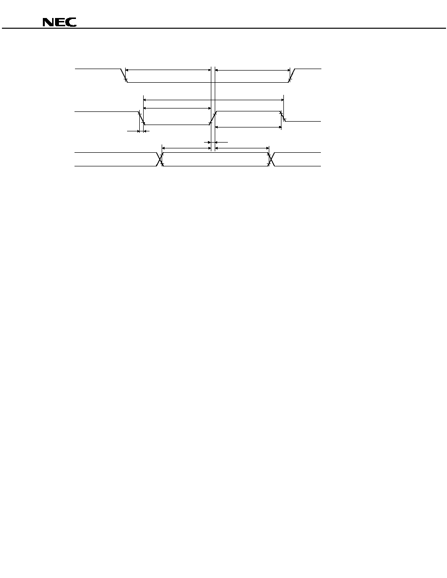
Preliminary Product Information S15797EJ1V4PM
48
µ
µ
µ
µ
PD161644
(b) Serial interface
t
CSS
t
CSH
GCS
t
SLW
t
f
t
SDS
t
SCYC
t
SHW
t
SDH
t
r
GCL
GDA

Preliminary Product Information S15797EJ1V4PM
49
µ
µ
µ
µ
PD161644
[MEMO]

Preliminary Product Information S15797EJ1V4PM
50
µ
µ
µ
µ
PD161644
[MEMO]
Preliminary Product Information S15797EJ1V4PM
51
µ
µ
µ
µ
PD161644
NOTES FOR CMOS DEVICES
1
PRECAUTION AGAINST ESD FOR SEMICONDUCTORS
Note:
Strong electric field, when exposed to a MOS device, can cause destruction of the gate oxide and
ultimately degrade the device operation. Steps must be taken to stop generation of static electricity
as much as possible, and quickly dissipate it once, when it has occurred. Environmental control
must be adequate. When it is dry, humidifier should be used. It is recommended to avoid using
insulators that easily build static electricity. Semiconductor devices must be stored and transported
in an anti-static container, static shielding bag or conductive material. All test and measurement
tools including work bench and floor should be grounded. The operator should be grounded using
wrist strap. Semiconductor devices must not be touched with bare hands. Similar precautions need
to be taken for PW boards with semiconductor devices on it.
2
HANDLING OF UNUSED INPUT PINS FOR CMOS
Note:
No connection for CMOS device inputs can be cause of malfunction. If no connection is provided
to the input pins, it is possible that an internal input level may be generated due to noise, etc., hence
causing malfunction. CMOS devices behave differently than Bipolar or NMOS devices. Input levels
of CMOS devices must be fixed high or low by using a pull-up or pull-down circuitry. Each unused
pin should be connected to V
DD
or GND with a resistor, if it is considered to have a possibility of
being an output pin. All handling related to the unused pins must be judged device by device and
related specifications governing the devices.
3
STATUS BEFORE INITIALIZATION OF MOS DEVICES
Note:
Power-on does not necessarily define initial status of MOS device. Production process of MOS
does not define the initial operation status of the device. Immediately after the power source is
turned ON, the devices with reset function have not yet been initialized. Hence, power-on does
not guarantee out-pin levels, I/O settings or contents of registers. Device is not initialized until the
reset signal is received. Reset operation must be executed immediately after power-on for devices
having reset function.