 | –≠–ª–µ–∫—Ç—Ä–æ–Ω–Ω—ã–π –∫–æ–º–ø–æ–Ω–µ–Ω—Ç: UPD16667 | –°–∫–∞—á–∞—Ç—å:  PDF PDF  ZIP ZIP |
DATA SHEET
MOS INTEGRATED CIRCUIT
µ
µ
µ
µ
PD16667
160-OUTPUT LCD ROW DRIVER
Document No. S12838EJ4V0DS00 (4th edition)
Date Published January 1999 N CP(K)
Printed in Japan
The mark shows major revised points.
The
µ
PD16667 is a row (common) driver which contains a RAM capable of full-dot LCD display. With 160 outputs,
this driver can be combined with a column (segment) driver,
µ
PD16662, which contains a RAM to display 240
◊
160
pixels to 480
◊
320 pixels.
With a built-in display RAM, the column driver can reduce the current consumption, thus making it most suitable
for the display block of a PDA or portable terminal.
FEATURES
∑
LCD-driven voltage: 20 to 36 V
∑
Duty: 1/160
∑
Driving type: 2 lines selected simultaneously
∑
Output count: 160 outputs
∑
Capable of gray scale display: 4 gray scales
ORDERING INFORMATION
Part No.
Package
µ
PD16667N-XXX
TCP (TAB)
µ
PD16667N-051
Standard TCP (OLB: 0.2 mm pitch, folding)
The external shape of the TCP is custom-made, so please contact an NEC sales representative with your shape
requirements.

2
µ
µ
µ
µ
PD16667
BLOCK DIAGRAM
Liquid-crystal drive circuit
Selection control circuit
Bidirectional shift register
Level shifter
X
1
to X
160
V
DD
V
1
V
EE
DIR
V
CC1
V
SS
L1
L2
/DOFF'
STB
/FRM
Column driver interface
Q
1
to Q
80
Remark
/xxx indicates active low signal.
BLOCK FUNCTION
1. Liquid-crystal drive circuit
This circuit selects and outputs the level for liquid-crystal driving.
One of V
DD
, V
EE
, and V
1
is selected by the output of the selection control circuit.
2. Selection control circuit
This circuit creates the signal which will select the level of the output signal, based on the output of the shift
register circuit and the driving level power selection signals L1 and L2
3. Bidirectional shift register circuit
This refers to the 80-bit bidirectional shift register circuit. The DIR signal can be used to switch over the shift
direction.
The data that has been entered from the /FRM pin is shifted by the low drive signal strobe (STB).
4. Level shifter circuit
This circuit transforms the 5-V signals to the high-voltage signals for liquid-crystal driving.
3
µ
µ
µ
µ
PD16667
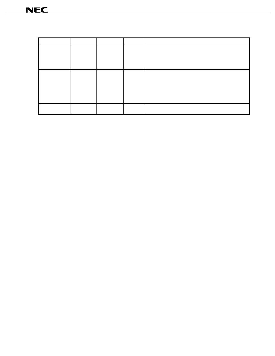
PIN FUNCTIONS
Classification
Pin Name
Input/Output
Pad No.
Function
Power suuply
V
CC1
V
SS
V
DD
V
EE
V
1
5 V power for level shifter
GND for level shifter
Power for logic, liquid-crystal drive level power
Power for logic, liquid-crystal drive level power (GND)
Liquid-crystal drive level power
Liquid-crystal
display timing
STB
/FRM
/DOFF'
L1
L2
DIR
I
I
I
I
I
I
Row drive signal strobe
Frame signal
Display OFF signal
Drive level power selection symbol (1st line)
Drive level power selection symbol (2nd line)
Shift direction selection symbol:when L (DIR = V
EE
), X
1
X
160
when H (DIR = V
DD
), X
160
X
1
Liquid-crystal
drive output
X
1
to X
160
O
Liquid-crystal drive output
Selects and outputs one of V
DD
, V
EE
, and V
1
.
DETAILS OF PIN FUNCTIONS
∑
STB (input)
Input pin of the row drive strobe signal
The bidirectional shift register is shifted at STB's rising edge.
∑
/FRM (input)
Input pin of the frame signal
The shift register data is read at STB's rising edge.
∑
DIR (input)
Input pin of the drive output's shift direction selection signal
When the shift direction selection signal (DIR) is "L", the shift data (selection signal) is shifted from the drive
output X
1
to the X
160
direction. When "H", it is shifted from the X
160
to the X
1
direction.
∑
/DOFF
'
(input)
Input pin of the display OFF signal
It is placed in the display OFF status (all outputs at V
1
) at the "L" level. In the mean time, it reads the frame signal
and returns to the normal display status at the "H" level.
∑
L1 and L2 (input)
Input pins of the drive level power selection signal
In the case of the liquid-crystal drive output, the two lines are selected simultaneously by the shift register. L1
selects the first line, and L2 selects the second line. Both lines select V
DD
at "H", and V
EE
at "L".
4
µ
µ
µ
µ
PD16667
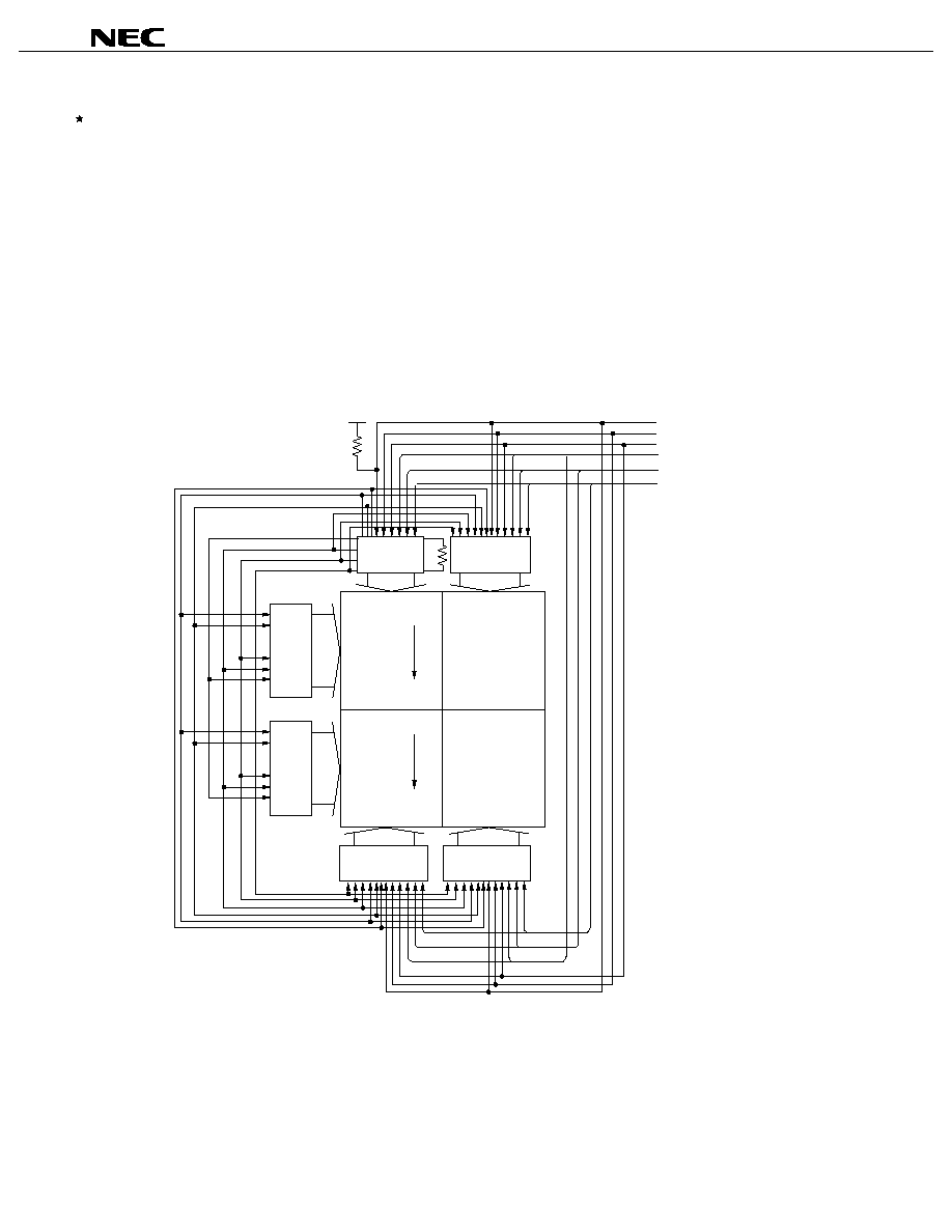
SYSTEM CONFIGURATION EXAMPLE
This example shows configuration of a liquid-crystal panel of half-VGA size (480 x 320 oblong) using four column
drivers and two row drivers.
∑
Each column driver sets the LSI No. with PL0 and PL1 pins.
∑
The DIR pins of each column driver are all set to low level.
∑
Only one of the column drivers is set to the master, all the others are set to the slave. Signals are supplied from
the master column driver to the slave column driver and the row driver.
∑
Connect an oscillator resistor to the OSC1 and OSC2 pins of the master, and leave the slave open.
∑
Inputs signals from the system (D0 to D15, A0 to A16, /CS, /OE, /WE, /UBE, RDY, /RESET, /DOFF') in parallel to
all of the column driver. Connect a pull-up resistor to the RDY signal.
∑
The TEST pin is used to test the LSI, and is open or GND when the system is configured.
Remark The /DOUT pin is an output pin for the column driver.
RDY
/DOFF
/RESET
D0 to D15
A0 to A16
Control
(/CS, /OE,
/WE, /UBE)
Master
No. 0
Slave
No. 2
Slave
No. 1
Slave
No. 3
OSC1
OSC2
160
160
Y1
Y1
Y240
Y240
Y1
Y240
Y1
Y240
PULSE
V
CC2
STB
/FRM
/REFRH
/DOUT, /DOFF'
L1
L2
Row driver
Scan direction
Scan direction
Row driver

5
µ
µ
µ
µ
PD16667
POWER SUPPLY SEQUENCE OF CHIP SET
It is recommended to apply power in the following sequence.
V
CC2
V
CC1
input
V
DD
, V
EE
V
1
, V
2
Be sure to apply LCD drive voltages V
1
and V
2
last.
V
CC2
OFF
ON
V
DD
Note 2
OFF
ON
OFF
ON
V
EE
Note 2
V
1
OFF
ON
V
2
OFF
ON
V
CC1
/RESET
CPU I/F
(A0 to A16, /CS,
/OE, /WE, /UBE,
D0 to D15, /DOFF)
OFF
ON
0 V
3.3 V
0 V
3.3 V
0.3 V
CC2
4.5 V
0 s or
more
0 s or
more
100 ns or
more
0 ns
or
more
Note 1
Note 1
Note 1
Note 1
Notes 1. V
CC2
, CPU I/F, /RESET, and V
2
are column driver power supply pins or input pins.
2. V
DD
and V
EE
do not need to be turned ON at the same time.
Caution Turn off the power to the chip set in the reverse order of the power application sequence.