Document Outline
- COVER
- FEATURES
- ORDERING INFORMATION
- FUNCTIONAL OUTLINE
- PIN CONFIGURATION (Top View)
- PIN NAME
- BLOCK DIAGRAM
- 1. PIN FUNCTIONS
- 1.1 Pin Function List
- 1.2 Equivalent Circuits of Pins
- 1.3 Connections of Unused Pins
- 1.4 Cautions on Using CE, INT0 through INT4, and RESET# Pins
- 1.5 Cautions on Using TEST Pin
- 2. PROGRAM MEMORY (ROM)
- 2.1 Outline of Program Memory
- 2.2 Program Memory
- 2.3 Program Counter
- 2.4 Flow of Program
- 2.5 Cautions on Using Program Memory
- 3. ADDRESS STACK (ASK)
- 3.1 Outline of Address Stack
- 3.2 Address Stack Register (ASR)
- 3.3 Stack Pointer (SP)
- 3.4 Operation of Address Stack
- 3.5 Cautions on Using Address Stack
- 4. DATA MEMORY (RAM)
- 4.1 Outline of Data Memory
- 4.2 Configuration and Function of Data Memory
- 4.3 Data Memory Addressing
- 4.4 Cautions on Using Data Memory
- 5. SYSTEM REGISTERS (SYSREG)
- 5.1 Outline of System Registers
- 5.2 System Register List
- 5.3 Address Register (AR)
- 5.4 Window Register (WR)
- 5.5 Bank Register (BANK)
- 5.6 Index Register (IX) and Data Memory Row Address Pointer (MP : memory pointer)
- 5.7 General Register Pointer (RP)
- 5.8 Program Status Word (PSWORD)
- 6. GENERAL REGISTER (GR)
- 6.1 Outline of General Register
- 6.2 General Register
- 6.3 Generating Address of General Register by Each Instruction
- 6.4 Cautions on Using General Register
- 7. ALU (Arithmetic Logic Unit) BLOCK
- 7.1 Outline of ALU Block
- 7.2 Configuration and Function of Each Block
- 7.3 ALU Processing Instruction List
- 7.4 Cautions on Using ALU
- 8. REGISTER FILE (RF)
- 8.1 Outline of Register File
- 8.2 Configuration and function of Register File
- 8.3 Control Registers
- 8.4 Port Input/Output Selection Registers
- 8.5 Cautions on Using Register File
- 9. DATA BUFFER (DBF)
- 9.1 Outline of Data Buffer
- 9.2 Data Buffer
- 9.3 Relationships between Peripheral Hardware and Data Buffer
- 9.4 Cautions on Using Data Buffer
- 10. DATA BUFFER STACK
- 10.1 Outline of Data Buffer Stack
- 10.2 Data Buffer Stack Register
- 10.3 Data Buffer Stack Pointer
- 10.4 Operation of Data Buffer Stack
- 10.5 Using Data Buffer Stack
- 10.6 Cautions on Using Data Buffer Stack
- 11. GENERAL-PURPOSE PORT
- 11.1 Outline of General-purpose Port
- 11.2 General-Purpose I/O Port (P0A, P0B, P0C, P1D, P2A, P2B, P2C, P2D, P3A, P3B, P3C, P3D)
- 11.3 General-Purpose Input Port (P0D, P1A, P1C)
- 11.4 General-Purpose Output Port (P1B)
- 12. INTERRUPT
- 12.1 Outline of Interrupt Block
- 12.2 Interrupt Control Block
- 12.3 Interrupt Stack Register
- 12.4 Stack Pointer, Address Stack Registers, and Program Counter
- 12.5 Interrupt Enable Flip-Flop (INTE)
- 12.6 Accepting Interrupt
- 12.7 Operations after Interrupt Has Been Accepted
- 12.8 Returning from Interrupt Routine
- 12.9 External Interrupts (CE and INT0 through INT4 pins)
- 12.10 Internal Interrupts
- 13. TIMERS
- 13.1 Outline of Timers
- 13.2 Basic Timer 0
- 13.3 Timer 0
- 13.4 Timer 1
- 13.5 Timer 2
- 13.6 Timer 3
- 14. A/D CONVERTER
- 14.1 Outline of A/D Converter
- 14.2 Input Selection Block
- 14.3 Compare Voltage Generation and Compare Blocks
- 14.4 Comparison Timing Chart
- 14.5 Using A/D Converter
- 14.6 Cautions on Using A/D Converter
- 14.7 Status at Reset
- 15. D/A CONVERTER (PWM mode)
- 15.1 Outline of D/A Converter
- 15.2 PWM Clock Selection Register
- 15.3 PWM Output Selection Block
- 15.4 Duty Setting Block
- 15.5 Clock Generation Block
- 15.6 D/A Converter Output Wave
- 15.7 Example of Using D/A Converter
- 15.8 Status at Reset
- 16. SERIAL INTERFACES
- 16.1 Outline of Serial Interfaces
- 16.2 Serial Interface 0
- 16.3 Serial Interface 1
- 17. PLL FREQUENCY SYNTHESIZER
- 17.1 Outline of PLL Frequency Synthesizer
- 17.2 Input Selection Block and Programmable Divider
- 17.3 Reference Frequency Generator
- 17.4 Phase Comparator (PHI-DET), Charge Pump, and Unlock FF
- 17.5 PLL Disabled Status
- 17.6 Using PLL Frequency Synthesizer
- 17.7 Status at Reset
- 18. FREQUENCY COUNTER
- 18.1 Outline of Frequency Counter
- 18.2 Input/Output Selection Block and Gate Time Control Block
- 18.3 Start/Stop Control Block and IF Counter
- 18.4 Using IF Counter
- 18.5 Using External Gate Counter
- 18.6 Status at Reset
- 19. BEEP
- 19.1 Outline of BEEP
- 19.2 I/O Selection Block and Output Selection Block
- 19.3 Clock Selection Block and Clock Generation Block
- 19.4 Output Waveform of BEEP
- 19.5 Status at Reset
- 20. STANDBY
- 20.1 Outline of Standby Function
- 20.2 Halt Function
- 20.3 Clock Stop Function
- 20.4 Device Operation in Halt and Clock Stop Status
- 20.5 Cautions on Processing of Each Pin in Halt and Clock Stop Status
- 20.6 Device Operation Control Function of CE Pin
- 21. RESET
- 21.1 Outline of Reset
- 21.2 CE Reset
- 21.3 Power-ON Reset
- 21.4 Relationship between CE Reset and Power-ON Reset
- 21.5 Reset by RESET# Pin
- 21.6 WDT&SP Reset
- 21.7 Power Failure Detection
- 22. INSTRUCTION SET
- 22.1 Outline of Instruction Set
- 22.2 Legend
- 22.3 Instruction List
- 22.4 Assembler (RA17K) Embedded Macro Instruction
- 23. RESERVED SYMBOLS
- 23.1 Data Buffer (DBF)
- 23.2 System Registers (SYSREG)
- 23.3 Port Registers
- 23.4 Register File (Control Registers)
- 23.5 Peripheral Hardware Registers
- 23.6 Others
- 24. ELECTRICAL CHARACTERISTICS
- 25. PACKAGE DRAWING
- 26. RECOMMENDED SOLDERING CONDITIONS
- APPENDIX A. CAUTIONS ON CONNECTING CRYSTAL RESONATOR
- APPENDIX B. DEVELOPMENT TOOLS

The mark
shows major revised points.
MOS INTEGRATED CIRCUIT
Document No. U11624EJ2V0DS00 (2nd edition)
Date Published December 1996 N
Printed in Japan
The
�
PD17704, 17705, 17707, 17708, and 17709 are 4-bit single-chip CMOS microcontrollers containing
hardware for digital tuning systems.
Provided with a wealth of hardware, these microcontrollers are available in many variations of ROM and RAM
capacities to support various applications.
Therefore, a high-performance, multi-function digital tuning system can be configured with only one chip.
In addition, a one-time PROM model,
�
PD17P709, which can be written only once and therefore is ideal for
program evaluation and small-scale production of a
�
PD17704, 17705, 17707, 17708, or 17709 system, is also
available.
FEATURES
�
PD17704
�
PD17705
�
PD17707
�
PD17708
�
PD17709
Program memory (ROM)
16K bytes
24K bytes
32K bytes
(8192
�
16 bits)
(12288
�
16 bits)
(16384
�
16 bits)
General Purpose data
672
�
4 bits
1120
�
4 bits
1776
�
4 bits
memory (RAM)
�
Instruction execution time
�
Many interrupts
1.78
�
s (with f
X
= 4.5-MHz crystal oscillator)
External
: 6 sources
�
PLL frequency synthesizer
Internal
: 6 sources
Dual modulus prescaler (130 MHz MAX.),
�
Power-ON reset, CE reset, and power failure
programmable divider, phase comparator, charge
detection circuit
pump
�
Supply voltage: V
DD
= 5 V
�
10 %
�
Abundant peripheral hardware units
General-purpose I/O ports, serial interfaces, A/D
converter, D/A converter (PWM output), BEEP
output, frequency counter
Unless otherwise specified, the
�
PD17709 is treated as the representative model in this document.
4-BIT SINGLE-CHIP MICROCONTROLLERS WITH DEDICATED
HARDWARE FOR DIGITAL TUNING SYSTEM
The information in this document is subject to change without notice.
�
PD17704, 17705, 17707, 17708, 17709
�
1996
DATA SHEET

�
PD17704, 17705, 17707, 17708, 17709
2
ORDERING INFORMATION
Part Number
Package
�
PD17704GC-
���
-3B9
80-pin plastic QFP (14
�
14 mm, 0.65 mm pitch)
�
PD17705GC-
���
-3B9
80-pin plastic QFP (14
�
14 mm, 0.65 mm pitch)
�
PD17707GC-
���
-3B9
80-pin plastic QFP (14
�
14 mm, 0.65 mm pitch)
�
PD17708GC-
���
-3B9
80-pin plastic QFP (14
�
14 mm, 0.65 mm pitch)
�
PD17709GC-
���
-3B9
80-pin plastic QFP (14
�
14 mm, 0.65 mm pitch)
Remark
���
indicates a ROM code number.
FUNCTIONAL OUTLINE
Part Number
�
PD17704
�
PD17705
�
PD17707
�
PD17708
�
PD17709
Item
Program memory (ROM)
16K bytes
24K bytes (12288
�
16 bits)
32K bytes (16384
�
16 bits)
(8192
�
16 bits)
General-purpose data memory (RAM)
672
�
4 bits
1120
�
4 bits
1176
�
4 bits
Instruction execution time
1.78
�
s (with f
X
= 4.5-MHz crystal oscillator)
General-purpose port
� I/O port
: 46 pins
� Input port : 12 pins
� Output port: 4 pins
Stack level
� Address stack : 15 levels
� Interrupt stack: 4 levels
� DBF stack
: 4 levels (can be manipulated via software)
Interrupt
� External: 6 sources (falling edge of CE pin, INT0 through INT4)
� Internal : 6 sources (timers 0 through 3, serial interfaces 0 and 1)
Timer
5 channels
� Basic timer (clock: 10, 20, 50, 100 Hz)
: 1 channel
� 8-bit timer with gate counter (clock: 1 k, 2 k, 10 k, 100 kHz) : 1 channel
� 8-bit timer (clock: 1 k, 2 k, 10 k, 100 kHz)
: 2 channels
� 8-bit timer multiplexed with PWM (clock: 440 Hz, 4.4 kHz)
: 1 channel
A/D converter
8 bits
�
6 channels (hardware mode and software mode selectable)
D/A converter (PWM)
3 channels (8-bit or 9-bit resolution selectable by software)
Output frequency: 4.4 kHz, 440 Hz (with 8-bit PWM selected)
2.2 kHz, 220 Hz (with 9-bit PWM selected)
Serial interface
2 units (3 channels)
� 3-wire serial I/O
: 2 channels
� 2-wire serial I/O/I
2
C bus : 1 channel
PLL frequency
Division mode
� Direct division mode (VCOL pin (MF mode) : 0.5 to 3 MHz)
synthesizer
� Pulse swallow mode (VCOL pin (HF mode) : 10 to 40 MHz)
(VCOH pin (VHF mode) : 60 to 130 MHz)
Reference frequency
13 types selectable (1, 1.25, 2.5, 3, 5, 6.25, 9, 10, 12.5, 18, 20, 25, 50 kHz)
Charge pump
Two error-out output pins (EO0, EO1)
Phase comparator
Unlock status detectable by program

3
�
PD17704, 17705, 17707, 17708, 17709
Part Number
�
PD17704
�
PD17705
�
PD17707
�
PD17708
�
PD17709
Item
Frequency counter
� Intermediate frequency (IF) measurement
P1C0/FMIFC pin : in FMIF mode 10 to 11 MHz
in AMIF mode 0.4 to 0.5 MHz
P1C1/AMIFC pin: in AMIF mode 0.4 to 0.5 MHz
� External gate width measurement
P2A1/FCG1, P2A0/FCG0 pin
BEEP output
2 pins
Output frequency: 1 kHz, 3 kHz, 4 kHz, 6.7 kHz (BEEP0 pin)
67 Hz, 200 Hz, 3 kHz, 4 kHz (BEEP1 pin)
Reset
� Power-ON reset (on power application)
� Reset by RESET pin
� Watchdog timer reset
Can be set only once on power application: 65536 instruction, 131072
instruction, or no-use selectable
� Stack pointer overflow/underflow reset
Can be set only once on power application: interrupt stack or address stack
selectable
� CE reset (CE pin low
high level)
CE reset delay timing can be set.
� Power failure detection function
Standby
� Clock stop mode (STOP)
� Halt mode (HALT)
Supply voltage
� PLL operation: V
DD
= 4.5 to 5.5 V
� CPU operation: V
DD
= 3.5 to 5.5 V
Package
80-pin plastic QFP (14
�
14 mm, 0.65 mm pitch)

�
PD17704, 17705, 17707, 17708, 17709
4
PIN CONFIGURATION (Top View)
80-pin plastic QFP (14
�
14 mm, 0.65 mm pitch)
�
PD17704GC-
���
-3B9
�
PD17705GC-
���
-3B9
�
PD17707GC-
���
-3B9
�
PD17708GC-
���
-3B9
�
PD17709GC-
���
-3B9
22
GND2
P0D3/AD3
P0D2/AD2
P0D1/AD1
P0D0/AD0
P1C3/AD5
P1C2/AD4
P1C1/AMIFC
P1C0/FMIFC
V
DD
1
VCOH
VCOL
GND1
EO0
EO1
TEST
P1D3
P1D2
P1D1/BEEP1
P1D0/BEEP0
INT2
P1A3/INT4
P1A2/INT3
P1A1
P1A0/TM0G
P3A3
P3A2
P3A1
P3A0
P3B3
P3B2
P3B1
P3B0
P2A2
P2A1/FCG1
P2A0/FCG0
P1B3
P1B2/PWM2
P1B1/PWM1
P1B0/PWM0
1
2
3
4
5
6
7
8
9
10
11
12
13
14
15
16
17
18
19
20
P0C2
P0C3
P2C0
P2C1
P2C2
P2C3
P3D0
P3D1
P3D2
P3D3
P3C0
P3C1
P3C2
P3C3
P2B0
P2B1
P2B2
P2B3
INT0
INT1
60
59
58
57
56
55
54
53
52
51
50
49
48
47
46
45
44
43
42
41
21
23 24 25 26 27 28 29 30 31 32 33 34 35 36 37 38 39 40
RESET
V
DD
0
CE
X
IN
X
OUT
GND0
REG
P2D0
P2D1
P2D2
P0B0/SI1
P0B1/SO1
P0B2/SCK1
P0B3/SI0
P0A0/SO0
P0A1/SCK0
P0A2/SCL
P0A3/SDA
P0C0
P0C1
80 79 78 77 76 75 74 73 72 71 70 69 68 67 66 65 64 63 62 61

5
�
PD17704, 17705, 17707, 17708, 17709
PIN NAME
AD0-AD5
: A/D converter input
AMIFC
: AM frequency counter input
BEEP0, BEEP1 : BEEP output
CE
: Chip enable
EO0, EO1
: Error-out output
FCG0, FGC1
: Frequency counter gate input
FMIFC
: FM frequency counter input
GND0-GND2
: Ground 0 to 2
INT0-INT4
: External interrupt input
PWM0-PWM2
: D/A converter output
P0A0-P0A3
: Port 0A
P0B0-P0B3
: Port 0B
P0C0-P0C3
: Port 0C
P0D0-P0D3
: Port 0D
P1A0-P1A3
: Port 1A
P1B0-P1B3
: Port 1B
P1C0-P1C3
: Port 1C
P1D0-P1D3
: Port 1D
P2A0-P2A2
: Port 2A
P2B0-P2B3
: Port 2B
P2C0-P2C3
: Port 2C
P2D0-P2D2
: Port 2D
P3A0-P3A3
: Port 3A
P3B0-P3B3
: Port 3B
P3C0-P3C3
: Port 3C
P3D0-P3D3
: Port 3D
REG
: CPU regulator
RESET
: Reset input
SCK0, SCK1
: 3-wire serial clock I/O
SCL
: 2-wire serial clock I/O
SDA
: 2-wire serial data I/O
SI0, SI1
: 3-wire serial data input
SO0, SO1
: 3-wire serial data output
TEST
: Test input
TM0G
: Timer 0 gate input
VCOH
: Local oscillation high input
VCOL
: Local oscillation low input
V
DD
0, V
DD
1
: Power supply
X
IN
, X
OUT
: Main clock oscillation

�
PD17704, 17705, 17707, 17708, 17709
6
BLOCK DIAGRAM
4
4
AD0/P0D0
AD5/P1C3
AD1/P0D1
AD2/P0D2
AD3/P0D3
AD4/P1C2
4
4
4
4
4
4
4
3
4
4
3
4
4
4
P0A0-P0A3
P0B0-P0B3
P0C0-P0C3
P0D0-P0D3
P1A0-P1A3
P1B0-P1B3
P1C0-P1C3
P1D0-P1D3
P2A0-P2A2
P2B0-P2B3
P2C0-P2C3
P2D0-P2D2
P3A0-P3A3
P3B0-P3B3
P3C0-P3C3
P3D0-P3D3
PWM2/P1B2
PWM0/P1B0
PWM1/P1B1
Port
A/D
Converter
D/A
Converter
8-bit
Timer3
Basic
Timer
RF
RAM
672
�
4 bits
( PD17704, 17705)
1120
�
4 bits
( PD17707, 17708)
1776
�
4 bits
( PD17709)
SYSREG
ALU
Instruction
Decoder
ROM
8192
�
16 bits
( PD17704)
12288
�
16 bits
( PD17705, 17707)
16384
�
16 bits
( PD17708, 17709)
Program Counter
Stack
VCOH
VCOL
EO0
EO1
PLL
SO0/P0A0
SCK0/P0A1
SCL/P0A2
SDA/P0A3
SI0/P0B3
SCK1/P0B2
SO1/P0B1
SI1/P0B0
BEEP0/P1D0
BEEP1/P1D1
INT0
INT1
INT2
INT3/P1A2
INT4/P1A3
FCG0/P2A0
FCG1/P2A1
FMIFC/P1C0
AMIFC/P1C1
TM0G/P1A0
X
IN
X
OUT
CE
RESET
V
DD
0, V
DD
1
REG
V
CPU
CPU
Peripheral
GND0-GND2
Serial
Interface0
Serial
Interface1
BEEP
Interrupt
Control
Frequency
Counter
8-bit
Timer0
Gate
Counter
8-bit
Timer1
8-bit
Timer2
OSC
Reset
Regulator
�
�
�
�
�
�

7
�
PD17704, 17705, 17707, 17708, 17709
TABLE OF CONTESNTS
1.
PIN FUNCTIONS .............................................................................................................................. 11
1.1
Pin Function List .................................................................................................................. 11
1.2
Equivalent Circuits of Pins .................................................................................................. 16
1.3
Connections of Unused Pins .............................................................................................. 21
1.4
Cautions on Using CE, INT0 through INT4, and RESET Pins ..........................................
23
1.5
Cautions on Using TEST Pin ............................................................................................... 23
2.
PROGRAM MEMORY (ROM) .......................................................................................................... 24
2.1
Outline of Program Memory ................................................................................................ 24
2.2
Program Memory .................................................................................................................. 25
2.3
Program Counter .................................................................................................................. 26
2.4
Flow of Program ................................................................................................................... 26
2.5
Cautions on Using Program Memory ................................................................................
29
3.
ADDRESS STACK (ASK) ................................................................................................................ 30
3.1
Outline of Address Stack ..................................................................................................... 30
3.2
Address Stack Register (ASR) ............................................................................................ 30
3.3
Stack Pointer (SP) ................................................................................................................ 32
3.4
Operation of Address Stack ................................................................................................ 33
3.5
Cautions on Using Address Stack ...................................................................................... 34
4.
DATA MEMORY (RAM) ................................................................................................................... 35
4.1
Outline of Data Memory ....................................................................................................... 35
4.2
Configuration and Function of Data Memory ...................................................................
38
4.3
Data Memory Addressing .................................................................................................... 42
4.4
Cautions on Using Data Memory ........................................................................................ 43
5.
SYSTEM REGISTERS (SYSREG) ................................................................................................... 44
5.1
Outline of System Registers ............................................................................................... 44
5.2
System Register List ............................................................................................................ 45
5.3
Address Register (AR) ......................................................................................................... 46
5.4
Window Register (WR) ......................................................................................................... 48
5.5
Bank Register (BANK) ......................................................................................................... 49
5.6
Index Register (IX) and Data Memory Row Address Pointer (MP: memory pointer) .... 50
5.7
General Register Pointer (RP) ............................................................................................. 52
5.8
Program Status Word (PSWORD) ....................................................................................... 54
6.
GENERAL REGISTER (GR) ............................................................................................................ 56
6.1
Outline of General Register ................................................................................................. 56
6.2
General Register .................................................................................................................. 56
6.3
Generating Address of General Register by Each Instruction ........................................
57
6.4
Cautions on Using General Register .................................................................................
57

�
PD17704, 17705, 17707, 17708, 17709
8
7.
ALU (Arithmetic Logic Unit) BLOCK ............................................................................................. 58
7.1
Outline of ALU Block .......................................................................................................... 58
7.2
Configuration and Function of Each Block .......................................................................
59
7.3
ALU Processing Instruction List ......................................................................................... 59
7.4
Cautions on Using ALU ....................................................................................................... 63
8. REGISTER FILE (RF) ........................................................................................................................ 64
8.1
Outline of Register File ........................................................................................................ 64
8.2
Configuration and Function of Register File ....................................................................
65
8.3
Control Registers ................................................................................................................. 66
8.4
Port Input/Output Selection Registers ..............................................................................
78
8.5
Cautions on Using Register File ......................................................................................... 84
9. DATA BUFFER (DBF) ....................................................................................................................... 85
9.1
Outline of Data Buffer .......................................................................................................... 85
9.2
Data Buffer ............................................................................................................................ 86
9.3
Relationships between Peripheral Hardware and Data Buffer ........................................
87
9.4
Cautions on Using Data Buffer ........................................................................................... 90
10. DATA BUFFER STACK ................................................................................................................... 91
10.1
Outline of Data Buffer Stack ................................................................................................ 91
10.2
Data Buffer Stack Register .................................................................................................. 91
10.3
Data Buffer Stack Pointer .................................................................................................... 93
10.4
Operation of Data Buffer Stack ........................................................................................... 94
10.5
Using Data Buffer Stack ...................................................................................................... 95
10.6
Cautions on Using Data Buffer Stack ................................................................................
95
11. GENERAL-PURPOSE PORT ........................................................................................................... 96
11.1
Outline of General-purpose Port ......................................................................................... 96
11.2
General-Purpose I/O Port (P0A, P0B, P0C, P1D, P2A, P2B, P2C, P2D, P3A, P3B,
P3C, P3D) .............................................................................................................................. 99
11.3
General-Purpose Input Port (P0D, P1A, P1C) ................................................................... 113
11.4
General-Purpose Output Port (P1B) .................................................................................. 116
12. INTERRUPT ..................................................................................................................................... 117
12.1
Outline of Interrupt Block .................................................................................................... 117
12.2
Interrupt Control Block ........................................................................................................ 119
12.3
Interrupt Stack Register ....................................................................................................... 133
12.4
Stack Pointer, Address Stack Registers, and Program Counter .................................... 137
12.5
Interrupt Enable Flip-Flop (INTE) ........................................................................................ 137
12.6
Accepting Interrupt .............................................................................................................. 138
12.7
Operations after Interrupt Has Been Accepted ................................................................ 143
12.8
Returning from Interrupt Routine ....................................................................................... 143
12.9
External Interrupts (CE and INT0 through INT4 pins) ...................................................... 144
12.10 Internal Interrupts ................................................................................................................ 147
13. TIMERS ............................................................................................................................................ 148
13.1
Outline of Timers .................................................................................................................. 148

9
�
PD17704, 17705, 17707, 17708, 17709
13.2
Basic Timer 0 ........................................................................................................................ 150
13.3
Timer 0 .................................................................................................................................. 163
13.4
Timer 1 .................................................................................................................................. 172
13.5
Timer 2 .................................................................................................................................. 179
13.6
Timer 3 .................................................................................................................................. 186
14. A/D CONVERTER ............................................................................................................................ 193
14.1
Outline of A/D Converter ..................................................................................................... 193
14.2
Input Selection Block ........................................................................................................... 194
14.3
Compare Voltage Generation and Compare Blocks ........................................................ 196
14.4
Comparison Timing Chart ................................................................................................... 199
14.5
Using A/D Converter ............................................................................................................ 200
14.6
Cautions on Using A/D Converter ...................................................................................... 201
14.7
Status at Reset ..................................................................................................................... 201
15. D/A CONVERTER (PWM mode) ...................................................................................................... 202
15.1
Outline of D/A Converter ..................................................................................................... 202
15.2
PWM Clock Selection Register ........................................................................................... 203
15.3
PWM Output Selection Block .............................................................................................. 204
15.4
Duty Setting Block ............................................................................................................... 207
15.5
Clock Generation Block ....................................................................................................... 211
15.6
D/A Converter Output Wave ................................................................................................ 211
15.7
Example of Using D/A Converter ........................................................................................ 214
15.8
Status at Reset ..................................................................................................................... 215
16. SERIAL INTERFACES ..................................................................................................................... 216
16.1
Outline of Serial Interfaces .................................................................................................. 216
16.2
Serial Interface 0 .................................................................................................................. 217
16.3
Serial Interface 1 .................................................................................................................. 245
17. PLL FREQUENCY SYNTHESIZER .................................................................................................. 255
17.1
Outline of PLL Frequency Synthesizer .............................................................................. 255
17.2
Input Selection Block and Programmable Divider ........................................................... 256
17.3
Reference Frequency Generator ......................................................................................... 260
17.4
Phase Comparator (
-DET), Charge Pump, and Unlock FF ............................................. 262
17.5
PLL Disabled Status ............................................................................................................ 266
17.6
Using PLL Frequency Synthesizer ..................................................................................... 267
17.7
Status at Reset ..................................................................................................................... 271
18. FREQUENCY COUNTER ................................................................................................................. 272
18.1
Outline of Frequency Counter ............................................................................................. 272
18.2
Input/Output Selection Block and Gate Time Control Block ........................................... 273
18.3
Start/Stop Control Block and IF Counter .......................................................................... 276
18.4
Using IF Counter .................................................................................................................. 283
18.5
Using External Gate Counter .............................................................................................. 285
18.6
Status at Reset ..................................................................................................................... 286

�
PD17704, 17705, 17707, 17708, 17709
10
19. BEEP ................................................................................................................................................ 287
19.1
Outline of BEEP .................................................................................................................... 287
19.2
I/O Selection Block and Output Selection Block .............................................................. 288
19.3
Clock Selection Block and Clock Generation Block ........................................................ 290
19.4
Output Waveform of BEEP .................................................................................................. 291
19.5
Status at Reset ..................................................................................................................... 291
20. STANDBY ........................................................................................................................................ 292
20.1
Outline of Standby Function ............................................................................................... 292
20.2
Halt Function ........................................................................................................................ 293
20.3
Clock Stop Function ............................................................................................................ 299
20.4
Device Operation in Halt and Clock Stop Status .............................................................. 301
20.5
Cautions on Processing of Each Pin in Halt and Clock Stop Status .............................. 301
20.6
Device Operation Control Function of CE Pin .................................................................. 303
21. RESET .............................................................................................................................................. 306
21.1
Outline of Reset .................................................................................................................... 306
21.2
CE Reset ............................................................................................................................... 307
21.3
Power-ON Reset ................................................................................................................... 313
21.4
Relationship between CE Reset and Power-ON Reset .................................................... 316
21.5
Reset by RESET Pin ............................................................................................................. 320
21.6
WDT&SP Reset ..................................................................................................................... 321
21.7
Power Failure Detection ...................................................................................................... 327
22. INSTRUCTION SET ......................................................................................................................... 332
22.1
Outline of Instruction Set .................................................................................................... 332
22.2
Legend .................................................................................................................................. 333
22.3
Instruction List ..................................................................................................................... 334
22.4
Assembler (RA17K) Embedded Macro Instruction .......................................................... 336
23. RESERVED SYMBOLS ................................................................................................................... 337
23.1
Data Buffer (DBF) ................................................................................................................. 337
23.2
System Registers (SYSREG) ............................................................................................... 337
23.3
Port Registers ....................................................................................................................... 338
23.4
Register File (Control Registers) ........................................................................................ 340
23.5
Peripheral Hardware Registers ........................................................................................... 345
23.6
Others .................................................................................................................................... 345
24. ELECTRICAL CHARACTERISTICS ................................................................................................ 346
25. PACKAGE DRAWING ..................................................................................................................... 349
26. RECOMMENDED SOLDERING CONDITIONS .............................................................................. 350
APPENDIX A. CAUTIONS ON CONNECTING CRYSTAL RESONATOR ........................................... 351
APPENDIX B. DEVELOPMENT TOOLS ............................................................................................... 352
11
�
PD17704, 17705, 17707, 17708, 17709
1. PIN FUNCTIONS
1.1 Pin Function List
Pin No.
Symbol
Function
Output Form
1
INT2
Edge-detectable vectored interrupt input pins. Rising or falling edge can be
�
41
INT1
specified.
42
INT0
2
P1A3/INT4
Port 1A multiplexed with external interrupt request signal input and event
�
3
P1A2/INT3
signal input pins.
4
P1A1
� P1A3 through P1A0
5
P1A0/TM0G
� 4-bit input port
� INT4, INT3
� Edge-detectable vectored interrupt
� TM0G
� Input for gate of 8-bit timer 0
At reset
With clock stopped
Power-ON reset
WDT&SP reset
CE reset
Input
Input
Retained
Retained
(P1A3 through P1A0)
(P1A3 through P1A0)
6
P3A3
4-bit I/O port.
CMOS
|
|
Can be set in input or output mode in 4-bit units.
push-pull
9
P3A0
At reset
With clock stopped
Power-ON reset
WDT&SP reset
CE reset
Input
Input
Retained
Retained
10
P3B3
4-bit I/O port.
CMOS
|
|
Can be set in input or output mode in 4-bit units.
push-pull
13
P3B0
At reset
With clock stopped
Power-ON reset
WDT&SP reset
CE reset
Input
Input
Retained
Retained
14
P2A2
Port 2A multiplexed with external gate counter input pins.
CMOS
15
P2A1/FCG1
� P2A2 through P2A0
push-pull
16
P2A0/FCG0
� 3-bit I/O port
� Can be set in input or output mode in 1-bit units.
� FCG1, FCG0
� Input for external gate counter
At reset
With clock stopped
Power-ON reset
WDT&SP reset
CE reset
Input
Input
Retained
Retained
(P2A2 through P2A0)
(P2A2 through P2A0)
(P2A2 through P2A0)
(P2A2 through P2A0)
�
PD17704, 17705, 17707, 17708, 17709
12
Pin No.
Symbol
Function
Output Form
17
P1B3
Port 1B multiplexed with D/A converter output pins.
N-ch
18
P1B2/PWM2
� P1B3 through P1B0
open-drain
|
|
� 4-bit output port
(12 V)
20
P1B0/PWM0
� PWM2 through P2M0
� 8- or 9-bit D/A converter output
At reset
With clock stopped
Power-ON reset
WDT&SP reset
CE reset
Outputs low level
Outputs low level
Retained
Retained
(P1B3 through P1B0)
(P1B3 through P1B0)
(P1B3 through P1B0)
21
GND2
Ground
�
33
GND1
75
GND0
22
P0D3/AD3
Port 0D multiplexed with A/D converter input pins
�
|
|
� P0D3 through P0D0
25
P0D0/AD0
� 4-bit input port
� Can be connected with pull-down resistor in 1-bit units.
� AD3 through AD0
� Analog input of A/D converter with 8-bit resolution
At reset
With clock stopped
Power-ON reset
WDT&SP reset
CE reset
Input with pull-down
Input with pull-down
Retained
Retained
resistor
resistor
(P0D3 through P0D0)
(P0D3 through P0D0)
26
P1C3/AD5
Port 1C multiplexed with A/D converter input and IF counter input pins.
�
27
P1C2/AD4
� P1C3 through P1C0
28
P1C1/AMIFC
� 4-bit input port
29
P1C0/FMIFC
� AD5, AD4
� Analog input to A/D converter with 8-bit resolution
� FMIFC, AMIFC
� Input to frequency counter
At reset
With clock stopped
Power-ON reset
WDT&SP reset
CE reset
Input
Input
� P1C3/AD5,
� P1C3/AD5,
(P1C3 through P1C0)
(P1C3 through P1C0)
P1C2/AD4
P1C2/AD4
retained
retained
� P1C1/AMIFC,
� P1C1/AMIFC,
P1C0/FMIFC
P1C0/FMIFC
input
input
(P1C1, P1C0)
(P1C1, P1C0)

13
�
PD17704, 17705, 17707, 17708, 17709
Pin No.
Symbol
Function
Output Form
30
V
DD
1
Power supply. Supply the same voltage to these pins.
�
79
V
DD
0
� With CPU and peripheral function operating: 4.5 to 5.5 V
� With CPU operating
: 3.5 to 5.5 V
� With clock stopped
: 2.2 to 5.5 V
31
VCOH
PLL local oscillation (VCO) frequency input.
�
32
VCOL
� VCOH
� Active with VHF mode selected by program; otherwise, pulled down.
� VCOL
� Active with HF or MW mode selected by program; otherwise, pulled down.
Because the input of these pins goes into an AC amplifier, cut the DC
component of the input signal with a capacitor.
34
EO0
Output from charge pump of PLL frequency synthesizer. Outputs the divided
CMOS
35
EO1
frequency of local oscillation and the result of comparison of the phase
3-state
difference of reference frequency.
At reset
With clock stopped
Power-ON reset
WDT&SP reset
CE reset
High-impedance
High-impedance
High-impendance
High-impedance
output
output
output
output
36
TEST
Test input pin.
�
Be sure to connect this pin to GND.
37
P1D3
Port 1D and BEEP output.
CMOS
38
P1D2
� P1D3 through P1D0
push-pull
39
P1D1/BEEP1
� 4-bit I/O port
40
P1D0/BEEP0
� Can be set in input or output mode in 1-bit units.
� BEEP1, BEEP0
� BEEP output
At reset
With clock stopped
Power-ON reset
WDT&SP reset
CE reset
Input
Input
Retained
Retained
(P1D3 through P1D0)
(P1D3 through P1D0)
(P1D3 through P1D0)
(P1D3 through P1D0)
43
P2B3
4-bit I/O Port.
CMOS
|
|
Can be set in input or output mode in 1-bit units.
push-pull
46
P2B0
At reset
With clock stopped
Power-ON reset
WDT&SP reset
CE reset
Input
Input
Retained
Retained
47
P3C3
4-bit I/O Port.
CMOS
|
|
Can be set in input or output mode in 4-bit units.
push-pull
50
P3C0
At reset
With clock stopped
Power-ON reset
WDT&SP reset
CE reset
Input
Input
Retained
Retained
�
PD17704, 17705, 17707, 17708, 17709
14
Pin No.
Symbol
Function
Output Form
51
P3D3
4-bit I/O Port.
CMOS
|
|
Can be set in input or output mode in 4-bit units.
push-pull
54
P3D0
At reset
With clock stopped
Power-ON reset
WDT&SP reset
CE reset
Input
Input
Retained
Retained
55
P2C3
4-bit I/O Port.
CMOS
|
|
Can be set in input or output mode in 4-bit units.
push-pull
58
P2C0
At reset
With clock stopped
Power-ON reset
WDT&SP reset
CE reset
Input
Input
Retained
Retained
59
P0C3
4-bit I/O Port.
CMOS
|
|
Can be set in input or output mode in 4-bit units.
push-pull
62
P0C0
At reset
With clock stopped
Power-ON reset
WDT&SP reset
CE reset
Input
Input
Retained
Retained
63
P0A3/DSA
Ports P0A and P0B are multiplexed with I/O of serial interface.
N-ch
64
P0A2/SCL
� P0A3 through P0A0
open-drain
65
P0A1/SCK0
� 4-bit I/O port
CMOS
66
P0A0/SO0
� Can be set in input or output mode in 1-bit units.
push-pull
67
P0B3/SI0
� P0B3 through P0B0
68
P0B2/SCK1
� 4-bit I/O port
69
P0B1/SO1
� Can be set in input or output mode in 1-bit units.
70
P0B0/SI1
� SDA, SCL
� Serial data and serial clock I/O of serial interface 0 in 2-wire serial I/O or
I
2
C bus mode
� SCK0, SO0, SI0
� Serial clock I/O, serial data output, and serial data input of serial interface
0 in 3-wire serial I/O mode
� SCK1, SO1, SI1
� Serial clock I/O, serial data output, serial data input of serial interface 1
in 3-wire serial I/O mode
At reset
With clock stopped
Power-ON reset
WDT&SP reset
CE reset
Input
Input
Retained
Retained
P0A3 through P0A0,
P0A3 through P0A0,
P0A3 through P0A0,
P0A3 through P0A0,
P0B3 through P0B0
P0B3 through P0B0
P0B3 through P0B0
P0B3 through P0B0
71
P2D2
3-bit I/O port.
CMOS
|
|
Can be set in input or output mode in 1-bit units.
push-pull
73
P2D0
At reset
With clock stopped
Power-ON reset
WDT&SP reset
CE reset
Input
Input
Retained
Retained
15
�
PD17704, 17705, 17707, 17708, 17709
Pin No.
Symbol
Function
Output Form
74
REG
CPU regulator.
�
Connect this pin to GND via 0.1-
�
F capacitor.
76
X
OUT
Ground pins of crystal resonator.
�
77
X
IN
78
CE
Device operation-selection, CE reset, and interrupt signal input pin.
�
� Device operation-select
When CE is high, PLL frequency synthesizer can operate.
When CE is low, PLL frequency synthesizer is automatically disabled
internally.
� CE reset
When CE goes high, device is reset at rising edge of internal basic timer
setting pulse. This pin also has reset timing delay function.
� Interrupt
Vectored interrupt occurs at falling edge of this pin.
80
RESET
Reset input
�

�
PD17704, 17705, 17707, 17708, 17709
16
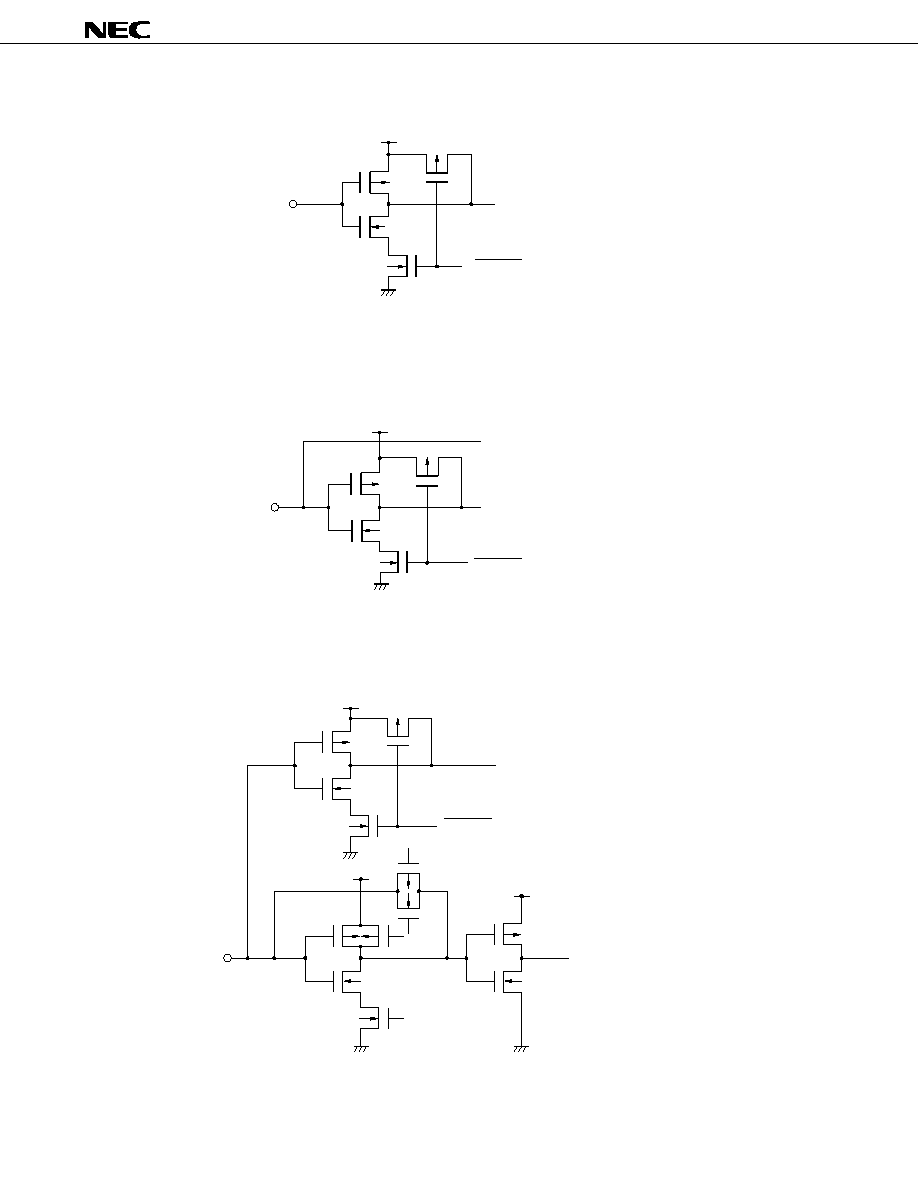
1.2 Equivalent Circuits of Pins
(1) P0A (P0A1/SCK0, P0A0/SO0)
P0B (P0B3/SI0, P0B2/SCK1, P0B1/SO1, P0B0/SI1)
P0C (P0C3, P0C2, P0C1, P0C0)
P1D (P1D3, P1D2, P1D1/BEEP1, P1D0/BEEP0)
P2A (P2A2, P2A1/FCG1, P2A0/FCG0)
P2B (P2B3, P2B2, P2B1, P2B0)
(I/O)
P2C (P2C3, P2C2, P2C1, P2C0)
P2D (P2D2, P2D1, P2D0)
P3A (P3A3, P3A2, P3A1, P3A0)
P3B (P3B3, P3B2, P3B1, P3B0)
P3C (P3C3, P3C2, P3C1, P3C0)
P3D (P3D3, P3D2, P3D1, P3D0)
Note
This is an internal signal that is output when the clock stop instruction is executed, and its circuit
is designed not to increase the current consumption due to noise even if it is floated.
V
DD
V
DD
CKSTOP
Note

17
�
PD17704, 17705, 17707, 17708, 17709
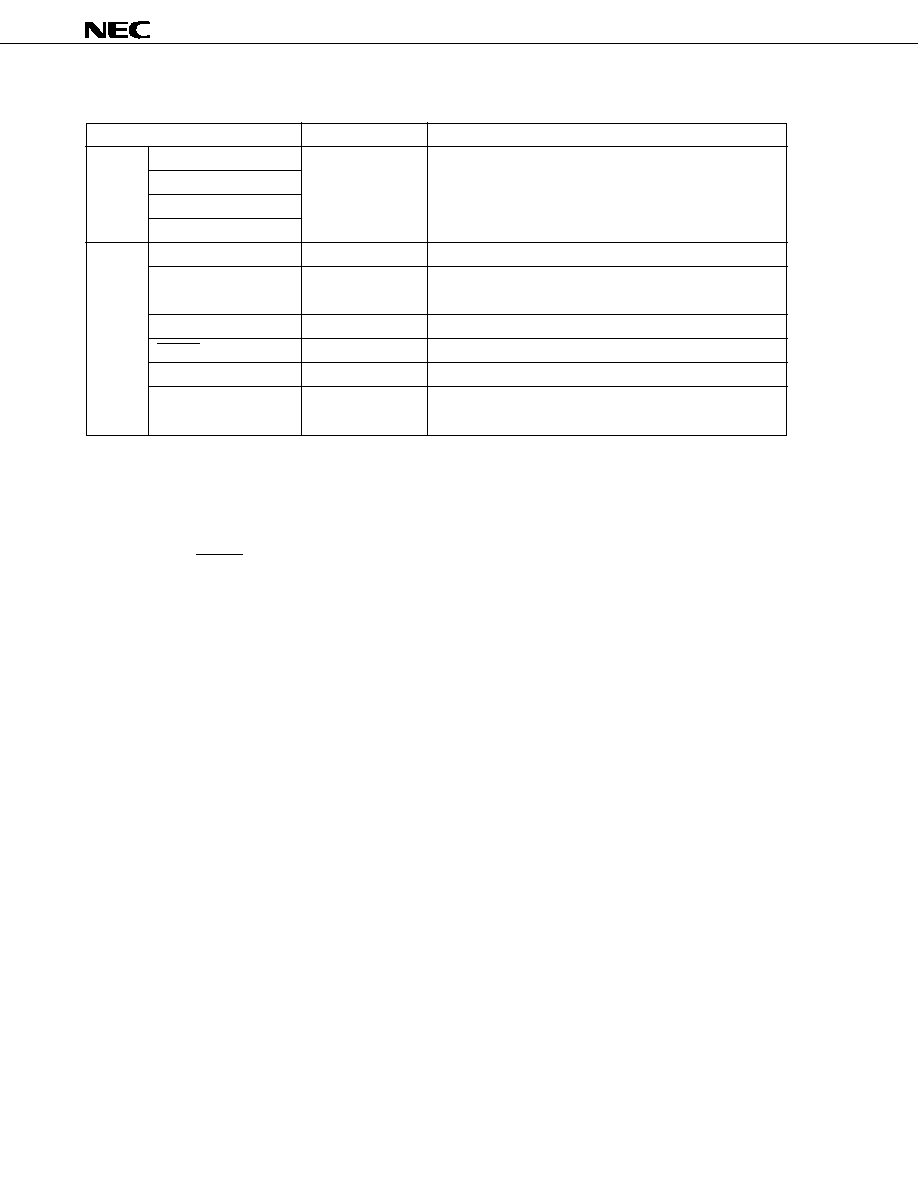
(2) P0A (P0A3/SDA, P0A2/SCL) (I/O)
Note
This is an internal signal that is output when the clock stop instruction is executed, and its circuit
is designed not to increase the current consumption due to noise even if it is floated.
(3) P1B (P1B3, P1B2/PWM2, P1B1/PWM1, P1B0/PWM0) (output)
(4) P0D (P0D3/AD3, P0D2/AD2, P0D1/AD1, P0D0/AD0) (input)
Note
This is an internal signal that is output when the clock stop instruction is executed, and its circuit
is designed not to increase the current consumption due to noise even if it is floated.
V
DD
CKSTOP
Note
V
DD
CKSTOP
Note
A/D converter
P0DPLD flag
High-ON resistance
�
PD17704, 17705, 17707, 17708, 17709
18
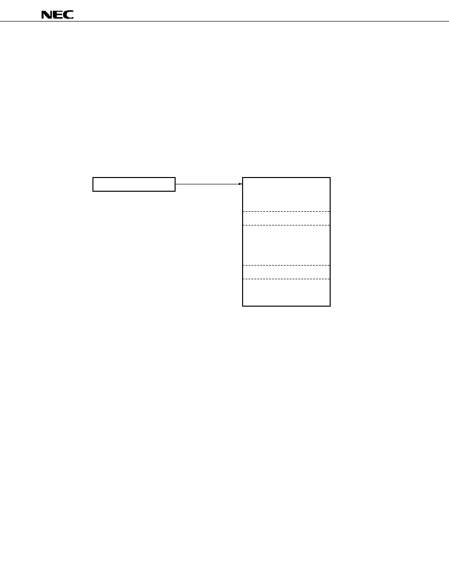
(5) P1A (P1A1) (input)
Note This is an internal signal output on execution of the clock stop instruction, and its circuit is
designed not to increase the current consumption due to noise even if the pin is floated.
(6) P1C (P1C3/AD5, P1C2/AD4) (input)
Note This is an internal signal output on execution of the clock stop instruction, and its circuit is
designed not to increase the current consumption due to noise even if the pin is floated.
(7) P1C (P1C1/AMIFC, P1C0/FMIFC) (input)
Note This is an internal signal output on execution of the clock stop instruction, and its circuit is
designed not to increase the current consumption due to noise even if the pin is floated.
V
DD
A/D converter
CKSTOP
Note
V
DD
CKSTOP
Note
V
DD
V
DD
V
DD
General-purpose port
High-ON resistance
Frequency counter
CKSTOP
Note

19
�
PD17704, 17705, 17707, 17708, 17709
(8) CE
RESET
INT0, INT1, INT2
(Schmitt trigger input)
P1A (P1A3/INT4, P1A2/INT3, P1A0/TM0G)
(9) X
OUT
(output), X
IN
(input)
(10) EO1, EO0 (output)
V
DD
V
DD
V
DD
High-ON
resistance
Internal clock
High-ON
resistance
X
IN
X
OUT
V
DD
DWN
UP

�
PD17704, 17705, 17707, 17708, 17709
20
(11) VCOH, VCOL (Input)
V
DD
V
DD
High-ON
resistance
High-ON
resistance

21
�
PD17704, 17705, 17707, 17708, 17709
1.3 Connections of Unused Pins
It is recommended to connect unused pins as follows:
Table 1-1. Connections of Unused Pins (1/2)
Pin Name
I/O Mode
Recommended Connections of Unused Pins
Port pin
P0D3/AD3-P0D0/AD0
Input
Individually connect to GND via resistor
Note 1
.
P1C3/AD5
P1C2/AD4
P1C1/AMIFC
Note 2
Set in port mode and individually connect to V
DD
or GND
P1C0/FMIFC
Note 2
via resistor
Note 1
.
P1A3/INT4
Individually connect to GND via resistor
Note 1
.
P1A2/INT3
P1A1
P1A0/TM0G
P1B3
N-ch open-drain
Set to low-level output by software and then open.
P1B2/PWM2-P1B0/PWM0
output
P0A3/SDA
I/O
Note 3
Set in general-purpose input port mode by software and
P0A2/SCL
individually connect to V
DD
or GND via resistor
Note 1
.
P0A1/SCK0
P0A0/SO0
P0B3/SI0
P0B2/SCK1
P0B1/SO1
P0B0/SI1
P0C3-P0C0
P1D3
P1D2
P1D1/BEEP1
P1D0/BEEP0
P2A2
P2A1/FCG1
P2A0/FCG0
P2B3-P2B0
P2C3-P2C0
P2D2-P2D0
Notes 1. If a pin is externally pulled up (connected to V
DD
via resistor) or pulled down (connected to GND
via resistor) with a high resistance, the pin almost enters a high-impedance state, increasing the
current (through-current) consumption of the port. Generally, the resistance of a pull-up or pull-
down resistor is several 10 k
, though it depends on the application circuit.
2. Do not set these pins as AMIFC and FMIFC pins; otherwise, the current consumption will increase.
3. The I/O ports are set in the general-purpose I/O port mode at power-ON reset, when reset by the
RESET pin, or when reset due to overflow or underflow of the watchdog timer or the stack.
�
PD17704, 17705, 17707, 17708, 17709
22
Table 1-1. Connections of Unused Pins (2/2)
Pin Name
I/O Mode
Recommended Connections of Unused Pins
Port pin
P3A3-P3A0
I/O
Note 2
Set in general-purpose input port mode by software and
P3B3-P3B0
individually connect to V
DD
or GND via resistor
Note 1
.
P3C3-P3C0
P3D3-P3D0
Pins other
CE
Input
Connect to V
DD
via resistor
Note 1
.
than port
EO1
Output
Open
pins
EO0
INT0-INT2
Input
Individually connect to GND via resistor
Note 1
.
RESET
Input
Connect to V
DD
via resistor
Note 1
.
TEST
�
Directly connect to GND.
VCOH
Input
Disable PLL via software and open.
VCOL
Notes 1. If a pin is externally pulled up (connected to V
DD
via resistor) or pulled down (connected to GND
via resistor) with a high resistance, the pin almost enters a high-impedance state, increasing the
current (through-current) consumption of the port. Generally, the resistance of a pull-up or pull-
down resistor is several 10 k
, though it depends on the application circuit.
2. The I/O ports are set in the general-purpose input port mode at power-ON reset, when reset by
the RESET pin, or when reset due to overflow or underflow of the watchdog timer or the stack.

23
�
PD17704, 17705, 17707, 17708, 17709
1.4 Cautions on Using CE, INT0 through INT4, and RESET Pins
The CE, INT0 through INT4, and RESET pins have a function to set a test mode in which the internal
operations of the
�
PD17709 are tested (IC test), in addition to the functions listed in 1.1 Pin Function List.
When a voltage exceeding V
DD
is applied to any of these pins, the device is set in the test mode. If a noise
exceeding V
DD
is superimposed during normal operation, therefore, the test mode is set by mistake, hindering
the normal operation.
Especially if the wiring length of pins is too long, noise is superimposed on these pins. In consequence,
the above problem occurs.
Therefore, keep the wiring length as short as possible to prevent noise from being superimposed. If
superimposition of noise is unavoidable, connect an external component as illustrated below to suppress the
noise.
� Connect a diode with low V
F
�
Connect a capacitor between a pin and V
DD
.
between a pin and V
DD
.
1.5 Cautions on Using TEST Pin
When V
DD
is applied to the TEST pin, the device is set in the test mode. Therefore, be sure to keep the wiring
length of this pin as short as possible, and directly connect it to the GND pin.
If the wiring length between the TEST pin and GND pin is too long, or if external noise is superimposed on
the TEST pin, generating a potential difference between the TEST pin and GND pin, your program may not run
normally.
CE, INT0-INT4, RESET
V
DD
CE, INT0-INT4, RESET
V
DD
Diode with
low V
F
V
DD
V
DD
GND TEST
Short
�
PD17704, 17705, 17707, 17708, 17709
24
2. PROGRAM MEMORY (ROM)
2.1 Outline of Program Memory
Figure 2-1 outlines the program memory.
As shown in this figure, the addresses of the program memory are specified by the program counter.
The program memory has the following two major functions.
�
To store programs
�
To store constant data
Figure 2-1. Outline of Program Memory
Instruction
Constant data
Program memory
Program counter
Address specification
...
...
...
...

25
�
PD17704, 17705, 17707, 17708, 17709
2.2 Program Memory
Figure 2-2 shows the configuration of the program memory.
As shown in this figure, the
�
PD17704 has 16K bytes (8192
�
16 bits) of program memory, the
�
PD17707
has 24K bytes (12288
�
16 bits), and the
�
PD17708 and 17709 have 32K bytes (16384
�
16 bits).
Therefore, the program memory addresses of the
�
PD17704 are 0000H through 1FFFH, those of the
�
PD17705, 17707 are 0000H through 2FFFH, and those of the
�
PD17708 and 17709 are 0000H through 3FFFH.
Because all "instructions" are "one-word instructions", one instruction can be stored to one address of the
program memory.
As constant data, the contents of the program memory are read to the data buffer by using a table reference
instruction.
Figure 2-2. Configuration of Program Memory
( PD17708, 17709)
16 bits
H
H
BR addr
instruction
branch
address
BR @AR instruction
branch address
CALL @AR instruction
subroutine entry address
MOVT DBF, @AR instruction
table reference address
Address
H
H
H
H
H
H
H
H
H
H
H
H
H
H
H
H
H
H
( PD17705, 17707)
Reset start address
Serial interface 1 interrupt vector
Serial interface 0 interrupt vector
Timer 3 interrupt vector
Timer 2 interrupt vector
Timer 1 interrupt vector
Timer 0 interrupt vector
INT4 pin interrupt vector
INT3 pin interrupt vector
INT2 pin interrupt vector
INT1 pin interrupt vector
INT0 pin interrupt vector
Falling edge interrupt vector of CE pin
Segment 0
Page 0
Page 1
Page 2
Page 3
Page 0
Page 1
Page 2
Page 3
CALL addr
instruction
subroutine
entry address
CALL addr
instruction
subroutine
entry address
BR addr
instruction
branch
address
Segment 1
(system
segment)
0
F
1
2
3
4
5
6
7
8
9
A
B
C
F
F
F
F
0
F
0
F
0
0
0
0
0
0
0
0
0
0
0
0
F
F
F
F
0
F
0
F
0
0
0
0
0
0
0
0
0
0
0
0
7
F
7
F
0
F
0
3
0
0
0
0
0
0
0
0
0
0
0
0
0
0
1
1
2
2
�
�
( PD17704)
�
�
PD17704, 17705, 17707, 17708, 17709
26
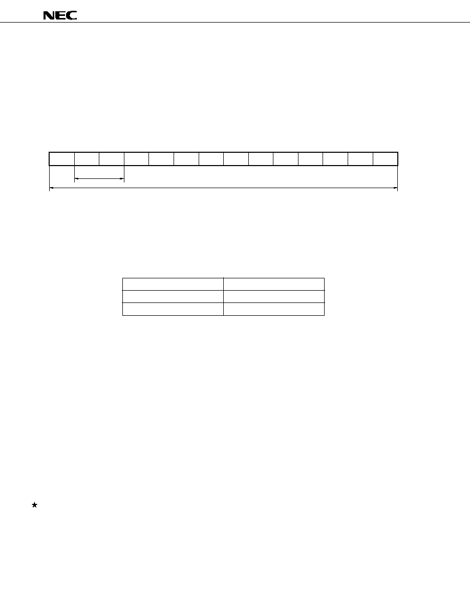
2.3 Program Counter
2.3.1 Configuration of program counter
Figure 2-3 shows the configuration of the program counter.
As shown in this figure, the program counter consists of a 13-bit binary counter and a 1-bit segment register
(SGR). Bits 11 and 12 of the program counter indicate a page.
The program counter specifies an address of the program memory.
Figure 2-3. Configuration of Program Counter
2.3.2 Segment register (SGR)
The segment register specifies a segment of the program memory.
Table 2-1 shows the relationships between the segment register and program memory.
The segment register is set only when the SYSCAL entry instruction is executed.
Table 2-1. Relationships between Segment Register and Program Memory
Value of Segment Register
Segment of Program Memory
0
Segment 0
1
Segment 1
2.4 Flow of Program
The flow of the program is controlled by the program counter that specifies an address of the program
memory.
The program flow when each instruction is executed is described below.
Figure 2-5 shows the value that is set to the program counter when each instruction is executed.
Table 2-2 shows the vector address when an interrupt is accepted.
2.4.1 Branch instruction
(1) Direct branch ("BR addr")
The branch destination address of the direct branch instruction is in the same segment of the program
memory. In other words, a branch cannot be executed exceeding a segment.
(2) Indirect branch ("BR @AR")
The branch destination addresses of the indirect branch instruction are all the addresses of the program
memory, i.e., addresses 0000H through 1FFFH for the
�
PD17704, addresses 0000H through 2FFFH for
the
�
PD17705, 17707, and 0000H through 3FFFH for the
�
PD17708 and 17709.
For further information, also refer to 5.3 Address Register (AR).
PC
0
SGR
Page
PC
PC
12
PC
11
PC
10
PC
9
PC
8
PC
7
PC
6
PC
5
PC
4
PC
3
PC
2
PC
1

27
�
PD17704, 17705, 17707, 17708, 17709
2.4.2 Subroutine
(1) Direct subroutine call ("CALL addr")
The first address of a subroutine that can be called by the direct subroutine instruction is in page 0 of
each segment (addresses 0000H through 07FFH).
(2) Indirect subroutine call (CALL @AR)
The first addresses of a subroutine that can be called by the indirect subroutine call instruction are all
the addresses of the program memory, i.e., addresses 000H through 1FFFH for the
�
PD17704,
addresses 0000H through 2FFFH for the
�
PD17705, 17707, and 0000H through 3FFFH for the
�
PD17708
and 17709.
For further information, also refer to 5.3 Address Register (AR).
2.4.3 Table reference
The addresses that can be referenced by the table reference instruction ("MOVT DBF, @AR") are all the
addresses of the program memory, i.e., addresses 0000H through 1FFFH for the
�
PD17704, addresses 0000H
through 2FFFH for the
�
PD17705, 17707, and 0000H through 3FFFH for the
�
PD17708 and 17709.
For further information, also refer to 5.3 Address Register (AR) and 9.2.2 Table reference instruction
(MOVT, DBF, @AR).
2.4.4 System call
The first address of a subroutine that can be called by the system call instruction ("SYSCAL entry") is the
first 16 steps of each block (block 0 to 7) in page 0 of segment 1 (system segment).
Figure 2-4. Outline of System Call Instruction
Page 1
Page 2
Page 3
Page 0
(16 bits
�
2K steps)
(16 bits
�
8K steps)
Segment 0
Page 1
Page 2
Page 3
(16 bits
�
8K steps)
Segment 1
(system segment)
Block 0
Block 1
Block 2
Block 7
Block 0 of segment 1
Entry address of
SYSCAL instruction
0
0
0
0
0
0
0
0
0
0
1
1
0
1
1
0
7
F
7
F
8
0
8
0
F
F
F
F
0
0
0
0
F
F
F
F
0
0
0
0
H
H
H
H
H
H
H
H
0
0
0
0
0
0
0
0
2
2
3
3
2
3
3
2
7
F
7
F
8
0
8
0
F
F
F
F
0
0
0
0
F
F
F
F
0
0
0
0
H
H
H
H
H
H
H
H
0 2 0 F F H
0 2 1 0 0 H
0 2 1 F F H
0 2 2 0 0 H
0 2 2 F F H
0 2 7 0 0 H
0 2 0 0 0 H
0 2 0 0 F H
Area where entry
address of system
segment can be
specified
.
.
.
.

�
PD17704, 17705, 17707, 17708, 17709
28
Figure 2-5. Value of Program Counter Upon Execution of Instruction
Table 2-2. Interrupt Vector Address
Order
Internal/External
Interrupt Source
Vector Address
1
External
Falling edge of CE pin
00CH
2
External
INT0 pin
00BH
3
External
INT1 pin
00AH
4
External
INT2 pin
009H
5
External
INT3 pin
008H
6
External
INT4 pin
007H
7
Internal
Timer 0
006H
8
Internal
Timer 1
005H
9
Internal
Timer 2
004H
10
Internal
Timer 3
003H
11
Internal
Serial interface 0
002H
12
Internal
Serial interface 1
001H
Contents of Program Counter (PC)
SGR
1
0
0
b
12
0
0
1
1
0
0
0
b
11
0
1
0
1
0
0
0
b
10
0
b
9
0
b
8
0
b
7
0
0
b
6
0
0
b
5
0
0
b
4
0
0
b
3
0
b
2
0
b
1
0
b
0
0
Program counter
Instruction
BR addr
CALL addr
SYSCAL entry
BR @AR
CALL @AR
MOVT DBF, @AR
RET
RETSK
RETI
Other instructions
(including skip instruction)
When interrupt is accepted
Power-ON reset,
watchdog timer reset,
RESET pin,
CE reset
Page 0
Page 1
Page 2
Page 3
entry
L
entry
H
Operand of instruction (addr)
Operand of instruction (addr)
Contents of address register
Re-
tained
Re-
tained
Contents of address stack register (ASR) (return address)
specified by stack pointer (SP)
Vector address of each interrupt
Increment
entry
H
: high-order 3 bits of entry
entry
L
: low-order 4 bits of entry
Re-
tained

29
�
PD17704, 17705, 17707, 17708, 17709
2.5 Cautions on Using Program Memory
2.5.1 Last address in each segment
The segment register is not connected to the binary counter.
Therefore, address 0000H of segment 0 is specified next to address 1FFFH, which is the last address of
segment 0.
To specify between segments, a dedicated instruction such as an indirect branch, indirect subroutine call,
or system call instruction is used.

�
PD17704, 17705, 17707, 17708, 17709
30
3. ADDRESS STACK (ASK)
3.1 Outline of Address Stack
Figure 3-1 outlines the address stack.
The address stack consists of a stack pointer and address stack registers.
The address of an address stack register is specified by the stack pointer.
The address stack saves a return address when a subroutine call instruction is executed or when an interrupt
is accepted.
The address stack is also used when the table reference instruction is executed.
Figure 3-1. Outline of Address Stack
3.2 Address Stack Register (ASR)
Figure 3-2 shows the configuration of the address stack register.
The address stack register consists of sixteen 16-bit registers ASR0 through ASR15. Actually, however, it
consists of fifteen 16-bit registers (ASR0 through ASR14) because no register is allocated to ASR15.
The address stack saves a return address when a subroutine is called, when an interrupt is accepted, and
when the table reference instruction is executed.
Stack pointer
Return address
Address stack register
Address specification

31
�
PD17704, 17705, 17707, 17708, 17709
Figure 3-2. Configuration of Address Stack Register
b
3
b
2
b
1
b
0
Stack pointer
(SP)
b
3
SP3
b
2
SP2
b
1
SP1
b
0
SP0
b
15
b
14
b
13
b
12
b
11
b
10
b
9
b
8
b
7
b
6
b
5
b
4
Bit
Address stack register (ASR)
Address
0H
1H
2H
3H
4H
5H
6H
7H
8H
9H
AH
BH
CH
DH
EH
FH
ASR0
ASR1
ASR2
ASR3
ASR4
ASR5
ASR6
ASR7
ASR8
ASR9
ASR10
ASR11
ASR12
ASR13
ASR14
ASR15 (Undefined)
Cannot be used
Bit

�
PD17704, 17705, 17707, 17708, 17709
32
3.3 Stack Pointer (SP)
3.3.1 Configuration and function of stack pointer
Figure 3-3 shows the configuration and functions of the stack pointer.
The stack pointer consists of a 4-bit binary counter.
It specifies the address of an address stack register.
A value can be directly read from or written to the stack pointer by using a register manipulation instruction.
Figure 3-3. Configuration and Function of Stack Pointer
Retained
Power-ON reset
WDT&SP reset
CE reset
Clock stop
Name
Flag symbol
b
3
S
P
3
b
2
S
P
2
b
1
S
P
1
b
0
S
P
0
Address
01H
Read/Write
R/W
Stack pointer
(SP)
0
0
0
0
0
0
0
0
1
1
1
1
1
1
1
1
1
1
1
0
1
0
1
0
1
0
1
0
1
0
1
0
1
0
1
1
1
1
Address 0 (ASR0)
Address 1 (ASR1)
Address 2 (ASR2)
Address 3 (ASR3)
Address 4 (ASR4)
Address 5 (ASR5)
Address 6 (ASR6)
Address 7 (ASR7)
Address 8 (ASR8)
Address 9 (ASR9)
Address 10 (ASR10)
Address 11 (ASR11)
Address 12 (ASR12)
Address 13 (ASR13)
Address 14 (ASR14)
Setting prohibited
Specifies address of address stack register (ASR)
0
0
0
0
1
1
1
1
0
0
0
0
1
1
1
1
1
1
1
0
0
1
1
0
0
1
1
0
0
1
1
0
0
1
1
1
1
1
(
At reset
(
(
(
Power-ON reset
WDT&SP reset
CE reset
Clock stop
: Reset by RESET pin up on power application
: Reset by watchdog timer and stack pointer
: CE reset
: Upon execution of clock stop instruction
(
(
(
(

33
�
PD17704, 17705, 17707, 17708, 17709
3.4 Operation of Address Stack
3.4.1 Subroutine call instruction ("CALL addr", "CALL @AR") and return instruction ("RET", "RETSK")
When a subroutine call instruction is executed, the value of the stack pointer is decremented by one, and
the return address is stored to an address stack register specified by the stack pointer.
When the return instruction is executed, the contents of the address stack register (return address) specified
by the stack pointer are restored to the program counter, and the value of the stack pointer is incremented by
one.
3.4.2 Table reference instruction ("MOVT DBF, @AR")
When the table reference instruction is executed, the value of the stack pointer is incremented by one, and
the return address is stored to an address stack register specified by the stack pointer.
Next, the contents of the program memory specified by the address register are read to the data buffer, the
contents of the address stack register (return value) specified by the stack pointer are restored to the program
counter, and the value of the stack pointer is incremented by one.
3.4.3 When interrupt is accepted and on execution of return instruction ("RETI")
When an interrupt is accepted, the value of the stack pointer is decremented by one, and the return address
is stored to an address stack register specified by the stack pointer.
When the return instruction is executed, the contents of an address stack register (return value) specified
by the stack pointer are restored to the program counter, and the value of the stack pointer is incremented by
one.
3.4.4 Address stack manipulation instruction ("PUSH AR", "POP AR")
When the "PUSH" instruction is executed, the value of the stack pointer is decremented by one, and the
contents of the address register are transferred to an address stack register specified by the stack pointer.
When the "POP" instruction is executed, the contents of an address stack register specified by the stack
pointer are transferred to the address register, and the value of the stack pointer is incremented by one.
3.4.5 System call instruction ("SYSCAL entry") and return instruction ("RET", "RETSK")
When the "SYSCAL entry" instruction is executed, the value of the stack pointer is decremented by one, and
the return address and the value of the segment register are stored to an address stack register specified by
the stack pointer.
When the return instruction is executed, the contents of an address stack register (return value) specified
by the stack pointer are restored to the program counter and segment register, and the value of the stack pointer
is incremented by one.

�
PD17704, 17705, 17707, 17708, 17709
34
3.5 Cautions on Using Address Stack
3.5.1 Nesting level and operation on overflow
The value of address stack register (ASR15) is "undefined" when the value of the stack pointer is 0FH.
Accordingly, if a subroutine call or system call exceeding 15 levels, or an interrupt is used without
manipulating the stack, execution returns to an "undefined" address.
3.5.2 Reset on detection of overflow or underflow of address stack
Whether the device is reset on detection of overflow or underflow of the address stack can be specified by
program. At reset, the program is started from address 0, and some control registers are initialized.
This reset function is valid at power-ON reset or reset by the RESET pin. For details, refer to 21. RESET.

35
�
PD17704, 17705, 17707, 17708, 17709
4. DATA MEMORY (RAM)
4.1 Outline of Data Memory
Figure 4-1 outlines the data memory.
As shown in the figure, system registers, a data buffer, port registers, and port input/output selection registers
are located on the data memory.
The data memory stores data, transfers data with the peripheral hardware or ports, and controls the CPU.
Figure 4-1. Outline of Data Memory (1/3)
(a)
�
PD17709
Note
Port input/output selection registers are allocated to addresses 60H through 6FH of BANK 15.
Peripheral hardware
Data transfer
Column address
Data memory
BANK0
Port registers
Port registers
Port registers
Port registers
BANK1
BANK2
BANK3
BANK4
BANK14
BANK15
Note
System registers
Ports
0
1
2
3
4
5
6
7
8
9
A
B
C
D
E
F
Data transfer
0
1
2
3
4
5
6
7
Data buffer
........
Row address
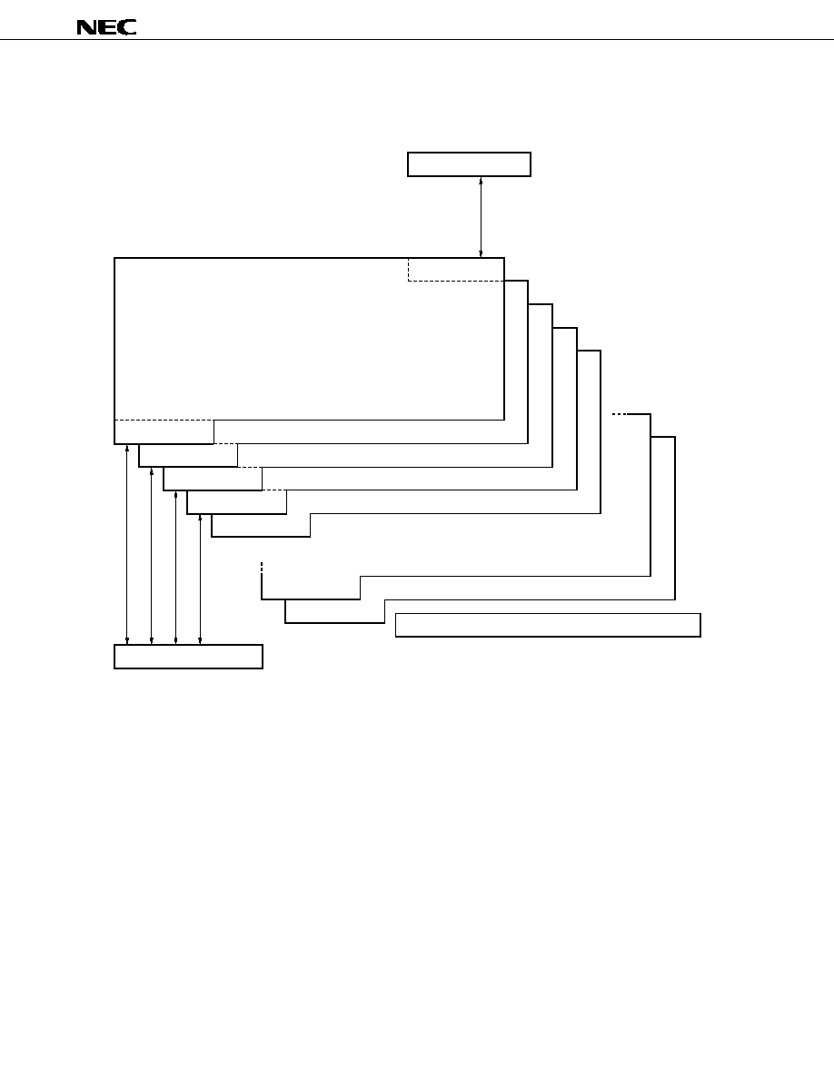
�
PD17704, 17705, 17707, 17708, 17709
36
Figure 4-1. Outline of Data Memory (2/3)
(b)
�
PD17707, 17708
Note
Port input/output selection registers are allocated to addresses 60H through 6FH of BANK 15.
Cautions 1. The
�
PD17707 and 17708 do not have BANKs 10 through 14.
2. Nothing is allocated to addresses 00H through 5FH of BANK15.
Peripheral hardware
Data transfer
Column address
Data memory
BANK0
Port registers
Port registers
Port registers
Port registers
BANK1
BANK2
BANK3
BANK4
BANK9
BANK15
Note
System registers
Ports
0
1
2
3
4
5
6
7
8
9
A
B
C
D
E
F
Data transfer
0
1
2
3
4
5
6
7
Data buffer
Row address
........

37
�
PD17704, 17705, 17707, 17708, 17709
Figure 4-1. Outline of Data Memory (3/3)
(c)
�
PD17704, 17705
Note
Port input/output selection registers are allocated to addresses 60H through 6FH of BANK 15.
Cautions 1. The
�
PD17704 and 17705 do not have BANKs 6 through 14.
2. Nothing is allocated to addresses 00H through 5FH of BANK15.
Peripheral hardware
Data transfer
Column address
Data memory
BANK0
Port registers
Port registers
Port registers
Port registers
BANK1
BANK2
BANK3
BANK4
BANK5
BANK15
Note
System registers
Ports
0
1
2
3
4
5
6
7
8
9
A
B
C
D
E
F
Data transfer
0
1
2
3
4
5
6
7
Data buffer
Row address

�
PD17704, 17705, 17707, 17708, 17709
38
4.2 Configuration and Function of Data Memory
Figure 4-2 shows the configuration of the data memory.
As shown in this figure, the data memory is divided into several banks with each bank made up of a total of
128 nibbles with 7H row addresses and 0FH column addresses.
The data memory can be divided into five functional blocks. Each block is described in 4.2.1 through 4.2.5
below.
The contents of the data memory can be operated on, compared, judged, and transferred in 4-bit units with
a single data memory manipulation instruction.
Table 4-1 lists the data memory manipulation instructions.
4.2.1 System registers (SYSREG)
The system registers are allocated to addresses 74H through 7FH.
Because the system registers are allocated to all banks, the same system registers exist at addresses 74H
through 7FH of any bank.
For details, refer to 5. SYSTEM REGISTER (SYSREG).
4.2.2 Data buffer (DBF)
The data buffer is allocated to addresses 0CH through 0FH of BANK 0.
For details, refer to 9. DATA BUFFER (DBF).
4.2.3 Port registers
The port registers are allocated to addresses 70H through 73H of BANKs 0 through 3.
For details, refer to 11. GENERAL-PURPOSE PORTS.
4.2.4 Port input/output selection registers
Port input/output selection registers are allocated to addresses 60H through 6FH of BANK15.
For details, refer to 8.4 Port Input/Output Selection Register.
4.2.5 General-purpose data memory
The general-purpose data memory is allocated to the addresses of the data memory excluding those of the
system registers, port registers, and port input/output selection registers.
(a)
�
PD17709
The general-purpose data memory of the
�
PD17709 consists of a total of 1776 nibbles of the 112 nibbles
each of BANKs 0 through 15 (BANK15 only has 96 nibbles).
(b)
�
PD17707, 17708
The general-purpose data memory of the
�
PD17707 and 17708 consists of a total of 1120 nibbles of the
112 nibbles each of BANKs 0 through 9.
(c)
�
PD17704, 17705
The general-purpose data memory of the
�
PD17704 and 17705 consists of a total of 672 nibbles of the
112 nibbles each of BANKs 0 through 5.

39
�
PD17704, 17705, 17707, 17708, 17709
Figure 4-2. Configuration of Data Memory (1/3)
(a)
�
PD17709
Note
An identical system register exists.
System registers
BANK0
Data memory
0
1
2
3
4
5
6
7
0
BANK1
Column address
0 1
0
1
2
3
4
5
6
7
General registers
System registers (SYSREG)
Note
Example
Address 51H
of BANK 0
b
3
b
2
b
1
b
0
0
1
2
3
4
5
6
7 Port register
System registers (SYSREG)
Note
0
1
2
3
4
5
6
7
0
1
2
3
4
5
6
7
System registers (SYSREG)
Note
System registers (SYSREG)
Note
1 2 3 4 5 6 7 8 9 A B C D E F
BANK2
BANK14
BANK15
2 3 4 5 6 7 8 9 A B C D E F
Data buffer
0 1 2 3 4 5 6 7 8 9 A B C D E F
0 1 2 3 4 5 6 7 8 9 A B C D E F
Fixed to 0
Column address
Fixed to 0
0 1 2 3 4 5 6 7 8 9 A B C D E F
BANK0
Column address
BANK1-BANK3
Column address
BANK4-BANK14
Column address
BANK15
Port register
Port input/output selection registers
Row address
...
Row address
Row address
Row address
Row address
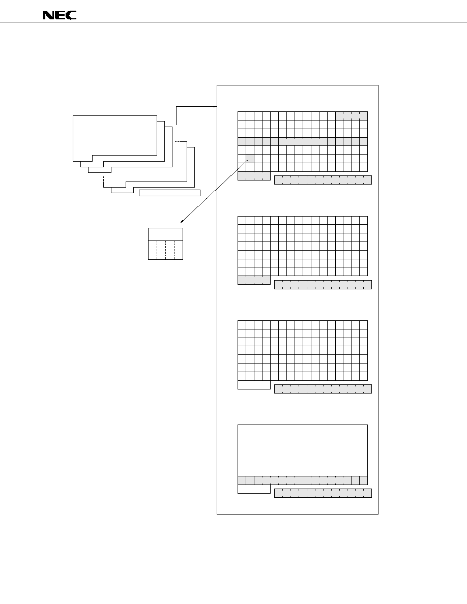
�
PD17704, 17705, 17707, 17708, 17709
40
Figure 4-2. Configuration of Data Memory (2/3)
(b)
�
PD17707, 17708
Note
An identical system register exists.
Cautions 1. The
�
PD17707 and 17708 do not have BANKs 10 through 14.
2. Nothing is allocated to addresses 00H through 5FH of BANK15.
System registers
BANK0
Data memory
0
1
2
3
4
5
6
7
0
BANK1
Column address
0 1
0
1
2
3
4
5
6
7
General registers
System registers (SYSREG)
Note
Example
Address 51H
of BANK 0
b
3
b
2
b
1
b
0
0
1
2
3
4
5
6
7 Port register
System registers (SYSREG)
Note
0
1
2
3
4
5
6
7
0
1
2
3
4
5
6
7
System registers (SYSREG)
Note
System registers (SYSREG)
Note
1 2 3 4 5 6 7 8 9 A B C D E F
BANK2
BANK9
BANK15
2 3 4 5 6 7 8 9 A B C D E F
Data buffer
0 1 2 3 4 5 6 7 8 9 A B C D E F
0 1 2 3 4 5 6 7 8 9 A B C D E F
Column address
Fixed to 0
0 1 2 3 4 5 6 7 8 9 A B C D E F
BANK0
Column address
BANK1-BANK3
Column address
BANK4-BANK9
Column address
BANK15
Port register
Fixed to 0
Port input/output selection registers
Nothing is allocated
...
Row address
Row address
Row address
Row address
Row address
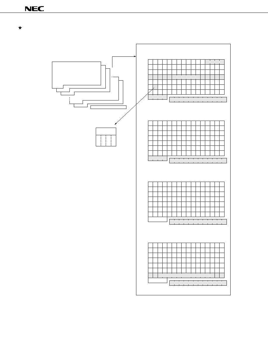
41
�
PD17704, 17705, 17707, 17708, 17709
Figure 4-2. Configuration of Data Memory (3/3)
(c)
�
PD17704, 17705
Note
An identical system register exists.
Cautions 1. The
�
PD17704 and 17705 do not have BANKs 6 through 14.
2. Nothing is allocated to addresses 00H through 5FH of BANK15.
System registers
BANK0
Data memory
0
1
2
3
4
5
6
7
0
BANK1
Column address
0 1
0
1
2
3
4
5
6
7
General registers
System registers (SYSREG)
Note
Example
Address 51H
of BANK 0
b
3
b
2
b
1
b
0
0
1
2
3
4
5
6
7 Port register
System registers (SYSREG)
Note
0
1
2
3
4
5
6
7
0
1
2
3
4
5
6
7
System registers (SYSREG)
Note
System registers (SYSREG)
Note
1 2 3 4 5 6 7 8 9 A B C D E F
BANK2
BANK5
BANK15
2 3 4 5 6 7 8 9 A B C D E F
Data buffer
0 1 2 3 4 5 6 7 8 9 A B C D E F
0 1 2 3 4 5 6 7 8 9 A B C D E F
Column address
Fixed to 0
0 1 2 3 4 5 6 7 8 9 A B C D E F
BANK0
Column address
BANK1-BANK3
Column address
BANK4, BANK5
Column address
BANK15
Port register
Fixed to 0
Port input/output selection registers
...
Row address
Row address
Row address
Row address
Row address

�
PD17704, 17705, 17707, 17708, 17709
42
Table 4-1. Data Memory Manipulation Instructions
Function
Instruction
Operation
Add
ADD
ADDC
Subtract
SUB
SUBC
Logic
AND
OR
XOR
Compare
SKE
SKGE
SKLT
SKNE
Transfer
MOV
LD
ST
Judge
SKT
SKF
4.3 Data Memory Addressing
Figure 4-3 shows address specification of the data memory.
An address of the data memory is specified by a bank, row address, and column address.
A row address and a column address are directly specified by a data memory manipulation instruction.
However, a bank is specified by the contents of a bank register.
For the details of the bank register, refer to 5. SYSTEM REGISTER (SYSREG).
Figure 4-3. Address Specification of Data Memory
Data memory address
Bank register
Column address
Row address
Bank
b
3
b
2
b
1
b
0
b
2
b
1
b
0
b
3
b
2
b
1
b
0
Instruction operand

43
�
PD17704, 17705, 17707, 17708, 17709
4.4 Cautions on Using Data Memory
4.4.1 At power-ON reset
The contents of the general-purpose data memory are "undefined" at power-ON reset.
Initialize the data memory as necessary.
4.4.2 Cautions on data memory not provided
If a data memory manipulation instruction that reads the data memory is executed to a data memory address
not provided, undefined data is read.
Nothing is changed even if data is written to such an address.

�
PD17704, 17705, 17707, 17708, 17709
44
5. SYSTEM REGISTERS (SYSREG)
5.1 Outline of System Registers
Figure 5-1 shows the location of the system registers on the data memory and their outline.
As shown in the figure, the system registers are allocated to addresses 74H through 7FH of all the banks
of the data memory. Therefore, identical system registers exist at addresses 74H through 7FH of any bank.
Because the system registers are located on the data memory, they can be manipulated by all data memory
manipulation instructions.
Seven types of system registers are available depending on function.
Figure 5-1. Location and Outline of System Registers on Data Memory
Column address
Data memory
BANK0
BANK1
BANK2
0
1
2
3
4
5
6
7
8
9
A
B
C
D
E
F
0
1
2
3
4
5
6
7
BANK14
BANK15
System register
Address
Name
Function
74H
75H
76H
77H
78H
79H
7AH
7BH
7CH
7DH
7EH
7FH
Address register
(AR)
Controls program memory address
Window
register
(WR)
Transfers
data with
register
file
Bank
register
(BANK)
Specifies
bank of
data
memory
Data memory row
address pointer (MP)
Index register
(IX)
Modifies address of data memory
General register
pointer (RP)
Specifies
address of
general register
Program
status
word
(PSWORD)
Controls
operation
Row address
......
Remark
�
The PD17704 and 17705 do not have the BANKs 6 through 14.
The PD17707 and 17708 do not have BANKs 10 through 14.
�

45
�
PD17704, 17705, 17707, 17708, 17709
5.2 System Register List
Figure 5-2 shows the configurations of the system registers.
Figure 5-2. Configuration of System Registers
Address
Name
Symbol
Bit
Data
74H
75H
76H
77H
78H
79H
7AH
7BH
7CH
7DH
7EH
7FH
Address register
(AR)
Window
register
(WR)
Bank
register
(BANK) Data memory row
address pointer (MP)
Index register
(IX)
General register
pointer (RP)
Program
status word
(PSWORD)
System registers
AR3
AR2
AR1
AR0
WR
BANK
IXH
MPH
IXM
MPL
IXL
RPH
RPL
PSW
b
2
b
1
b
0
b
3
b
3
b
2
b
1
b
0
b
3
b
2
b
1
b
0
b
3
b
2
b
1
b
0
b
3
b
2
b
1
b
0
b
3
b
2
b
1
b
0
b
3
b
2
b
1
b
0
M
P
E
0
b
3
b
2
b
1
b
0
b
3
b
2
b
1
b
0
b
3
b
2
b
1
b
0
b
3
b
2
b
1
b
0
B
C
D
b
3
b
2
b
1
b
0
C
M
P
C
Y
Z I
X
E
(RP)
(IX)
(MP)

�
PD17704, 17705, 17707, 17708, 17709
46
5.3 Address Register (AR)
5.3.1 Configuration of address register
Figure 5-3 shows the configuration of the address register.
As shown in the figure, the address register consists of 16 bits of system register addresses 74H through
77H (AR3 through AR0).
Figure 5-3. Configuration of Address Register
Address
Name
Symbol
Bit
Data
74H
AR3
75H
AR2
76H
AR1
77H
AR0
b
3
M
S
B
b
2
b
1
b
0
b
3
b
2
b
1
b
0
b
3
b
2
b
1
b
0
b
3
b
2
b
1
b
0
L
S
B
Power-ON reset
WDT&SP reset
CE reset
Clock stop
Address register (AR)
At reset
0
0
0
Retained
0
0
0
Retained
0
0
0
Retained
0
0
0
Retained
Power-ON reset
WDT&SP reset
CE reset
Clock stop
: Reset by RESET pin on power application
: Reset by watchdog timer and stack pointer
: CE reset
: On execution of clock stop instruction

47
�
PD17704, 17705, 17707, 17708, 17709
5.3.2 Function of address register
The address register specifies a program memory address when the table reference instruction ("MOVT DBF,
@AR"), stack manipulation instruction ("PUSH AR", "POP AR"), indirect branch instruction ("BR @AR"), or
indirect subroutine call instruction ("CALL @AR") is executed.
A dedicated instruction ("INC AR") is available that can increment the contents of the address instruction by
one.
The following paragraphs (1) through (5) describe the operation of the address register when the respective
instructions are executed.
(1) Table reference instruction ("MOVT DBF, @AR")
When the table reference instruction is executed, the constant data (16 bits) of a program memory
address specified by the contents of the address register are read to the data buffer.
The constant data that can be specified by the address register is stored to address 0000H to 1FFFH
in the case of
�
PD17704, address 0000H to 2FFFH in the case of the
�
PD17705 and 17707, and address
0000H to 3FFFH in the case of the
�
PD17708 and 17709.
(2) Stack manipulation instruction ("PUSH AR", "POP AR")
When the "PUSH AR" instruction is executed, the value of the stack pointer is decremented by one, and
the contents of the address register (AR) are transferred to an address stack register specified by the
stack pointer whose value has been decremented by one.
When the "POP AR" instruction is executed, the contents of an address stack register specified by the
stack pointer are transferred to the address register, and the value of the stack pointer is incremented
by one.
(3) Indirect branch instruction ("BR @AR")
When this instruction is executed, the program branches to a program memory address specified by the
contents of the address register.
The branch address that can be specified by the address register is 0000H to 1FFFH in the case of
�
PD17704, 0000H to 2FFFH in the case of the
�
PD17705 and 17707, and 0000H to 3FFFH in the case
of the
�
PD17705 and 17708 and 17709.
(4) Indirect subroutine call instruction ("CALL @AR")
The subroutine at a program memory address specified by the contents of the address register can be
called.
The first address of the subroutine that can be specified by the address register is 0000H to 1FFFH in
the case of the
�
PD17704, 0000H to 2FFFH in the case of the
�
PD17705 and 17707, and 0000H to 3FFFH
in the case of the
�
PD17708 and 17709.
(5) Address register increment instruction ("INC AR")
This instruction increments the contents of the address register by one.
5.3.3 Address register and data buffer
The address register can transfer data as part of the peripheral hardware via the data buffer.
For details, refer to 9. DATA BUFFER (DBF).
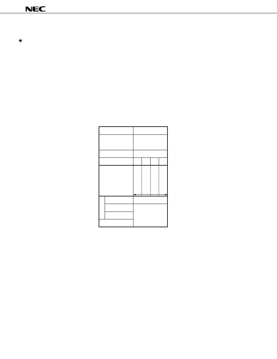
�
PD17704, 17705, 17707, 17708, 17709
48
5.3.4 Cautions on Using Address Register
Because the address register is configured in 16 bits, it can specify an address up to FFFFH.
However, the program memory exists at addresses 0000H to 1FFFH in the case of
�
PD17704, 0000H to
2FFFH in the case of the
�
PD17705 and 17707 and 0000H to 3FFFH in the case of the
�
PD17708 and 17709.
Therefore, the maximum value that can be set to the address register of the
�
PD17704 is address 1FFFH.
In the case of the
�
PD17705 and 17707, it is address 2FFFH. In the case of the
�
PD17708 and 17709, it is
address 3FFFH.
5.4 Window Register (WR)
5.4.1 Configuration of window register
Figure 5-4 shows the configuration of the window register.
As shown in the figure, the window register consists of 4 bits of system register address 78H (WR).
Figure 5-4. Configuration of Window Register
5.4.2 Function of window register
The window register is used to transfer data with the register file (RF) to be described later.
Data transfer between the window register and register file is manipulated by using dedicated instructions
"PEEK WR, rf" and "POKE, rf WR" (rf: address of register file).
The following paragraphs (1) and (2) describe the operation of the window register when these instructions
are executed.
For further information, also refer to 8. REGISTER FILE (RF).
(1) "PEEK WR, rf" instruction
When this instruction is executed, the contents of the register file addressed by "rf" are transferred to
the window register.
(2) "POKE rf, WR" instruction
When this instruction is executed, the contents of the window register are transferred to the register file
addressed by "rf".
Address
Name
Symbol
Bit
Data
Clock stop
78H
Window register
(WR)
WR
Undefined
Retained
b
3
M
S
B
b
2
b
1
b
0
L
S
B
Power-ON reset
WDT&SP reset
CE reset
At reset
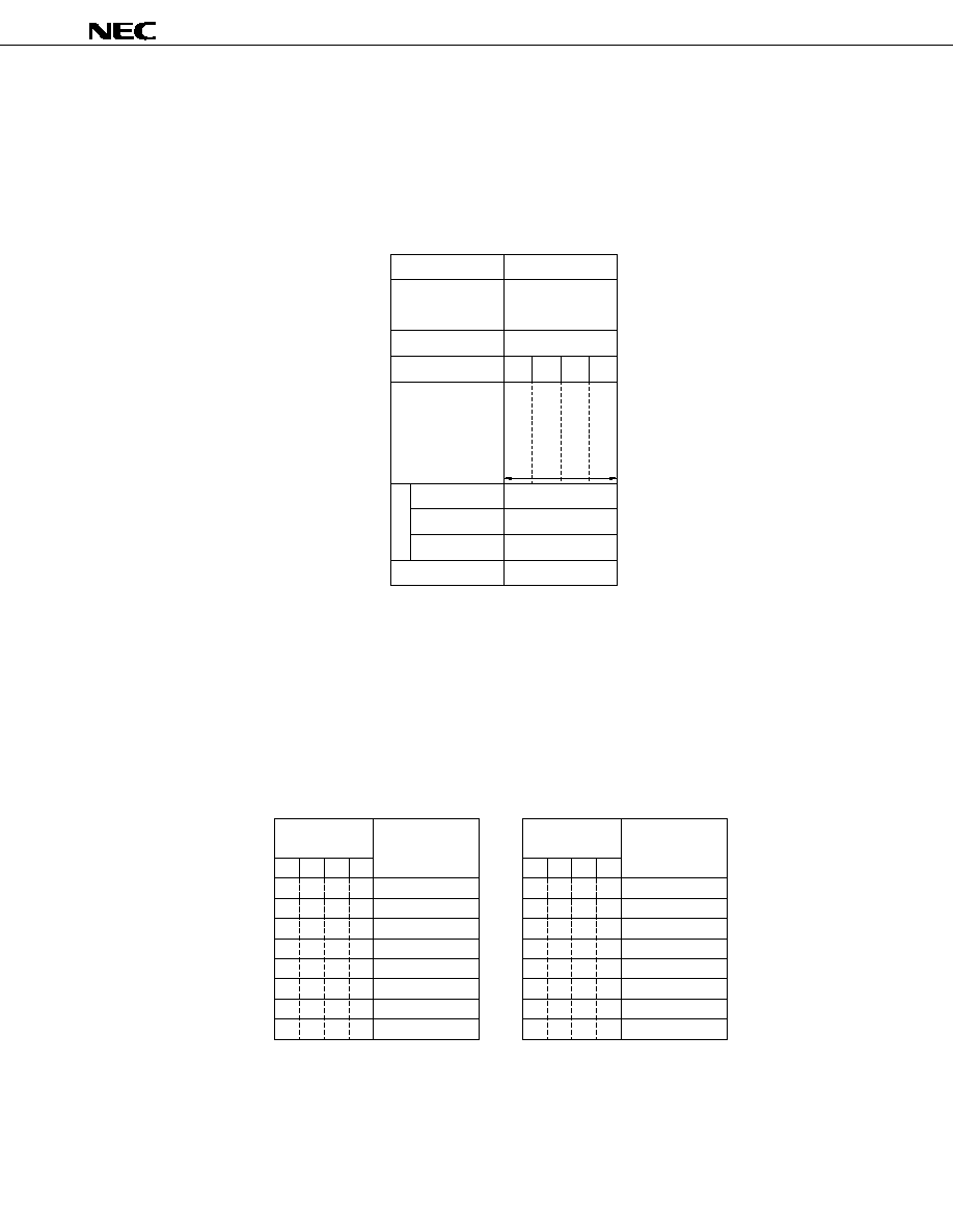
49
�
PD17704, 17705, 17707, 17708, 17709
5.5 Bank Register (BANK)
5.5.1 Configuration of bank register
Figure 5-5 shows the configuration of the bank register.
As shown in the figure, the bank register consists of 4 bits of system register address 79H (BANK).
Figure 5-5. Configuration of Bank Register
5.5.2 Function of bank register
The bank register specifies a bank of the data memory.
Table 5-1 shows the relationships between the value of the bank register and a bank of the data memory that
is specified.
Because the bank register is one of the system registers, its contents can be rewritten regardless of the bank
currently specified.
When manipulating a bank register, therefore, the status of the bank at that time is irrelevant.
Table 5-1. Data Memory Bank Specification
Note
Do not set BANKs 6 through 14 in the
�
PD17704 and 17705, and BANKs 10 through 14 in the
�
PD17707 and 17708 because these banks are not provided.
Caution
The area to which the data memory is allocated differs depending on the model. For details,
refer to Figure 4-2 Configuration of Data Memory.
Address
Name
Symbol
Bit
Data
Clock stop
79H
Bank register
(BANK)
BANK
0
0
0
Retained
b
3
M
S
B
b
2
b
1
b
0
L
S
B
Power-ON reset
WDT&SP reset
CE reset
At reset
Bank Register
(BANK)
Bank of Data
Memory
b
3
b
2
b
1
b
0
0
0
0
0
0
0
0
0
0
0
0
0
1
1
1
1
0
0
1
1
0
0
1
1
0
1
0
1
0
1
0
1
BANK0
BANK1
BANK2
BANK3
BANK4
BANK5
BANK6
Note
BANK7
Note
Bank Register
(BANK)
Bank of Data
Memory
b
3
b
2
b
1
b
0
1
1
1
1
1
1
1
1
0
0
0
0
1
1
1
1
0
0
1
1
0
0
1
1
0
1
0
1
0
1
0
1
BANK8
Note
BANK9
Note
BANK10
Note
BANK11
Note
BANK12
Note
BANK13
Note
BANK14
Note
BANK15

�
PD17704, 17705, 17707, 17708, 17709
50
5.6 Index Register (IX) and Data Memory Row Address Pointer (MP: memory pointer)
5.6.1 Configuration of index register and data memory row address pointer
Figure 5-6 shows the configuration of the index register and data memory row address pointer.
As shown in the figure, the index register consists of an index register (IX) made up of 11 bits (the low-order
3 bits (IXH) of system register address 7AH, and 7BH and 7CH (IXM, IXL)) and an index enable flag (IXE) at
the lowest bit position of 7FH (PSW).
The data memory row address pointer (memory pointer) consists of a data memory row address pointer (MP)
that is made up of 7 bits of the low-order 3 bits of 7AH (MPH) and 7BH (MPL), and a data memory row address
pointer enable flag (memory pointer enable flag: MPE) at the lowest bit position of 7AH (MPH).
In other words, the high-order 7 bits of the index register are shared with the data memory row address pointer
Figure 5-6. Configuration of Index Register and Data Memory Row Address Pointer
Address
Name
Symbol
Bit
Data
Clock stop
7AH
IXH
MPH
0
0
0
Retained
7BH
Index register (IX)
IXM
MPL
0
0
0
Retained
7CH
IXL
0
0
0
Retained
7EH
7FH
PSW
Memory pointer (MP)
b
3
M
P
E
b
2
M
S
B
M
S
B
b
1
b
0
b
3
b
2
b
1
b
0
L
S
B
b
3
b
2
b
1
b
0
L
S
B
b
3
b
2
b
1
b
0
b
3
b
2
b
1
b
0
I
X
E
0
0
0
R
Power-ON reset
WDT&SP reset
CE reset
IX
Program status word
(PSWORD)
MP
At reset
R: retained

51
�
PD17704, 17705, 17707, 17708, 17709
5.6.2 Functions of index register and data memory row address pointer
The index register and data memory row address pointer modify the addresses of the data memory.
The following paragraphs (1) and (2) describe their functions.
A dedicated instruction ("INC IX") that increments the value of the index register by one is available.
For the details of address modification, refer to 7. ALU (Arithmetic Logic Unit) BLOCK.
(1) Index register (IX)
When a data memory manipulation instruction is executed, the data memory address is modified by the
contents of the index register.
This modification, however, is valid only when the IXE flag is set to 1.
To modify the address, the bank, row address, and column address of the data memory are ORed with
the contents of the index register, and the instruction is executed to a data memory address (called real
address) specified by the result of this OR operation.
All data memory manipulation instructions are subject to address modification by the index register.
The following instructions, however, are not subject to address modification by the index register.
INC
AR
RORC
r
INX
IX
CALL
addr
MOVT
DBF, @AR
CALL
@AR
PUSH
AR
RET
POP
AR
RETSK
PEEK
WR,rf
RETI
POKE
rf,WR
EI
GET
DBF,p
DI
PUT
p, DBF
STOP s
BR
addr
HALT h
BR
@AR
NOP
(2) Data memory row address pointer (MP)
When the general register indirect transfer instruction ("MOV @r,m" or "MOV m,@r") is executed, the
indirect transfer destination address is modified.
This modification, however, is valid only when the MPE flag is set to 1.
To modify the address, the bank and row address at the indirect transfer destination are replaced by the
contents of the data memory row address pointer.
Instructions other than the general register indirect transfer instruction are not subject to address
modification.
(3) Index register increment instruction ("INC IX")
This instruction increments the contents of the index register by one.
Because the index register is configured of 10 bits, its contents are incremented to "000H" if the "INC
IX" instruction is executed when the contents of the index register are "3FFH".

�
PD17704, 17705, 17707, 17708, 17709
52
5.7 General Register Pointer (RP)
5.7.1 Configuration of General Register Pointer
Figure 5-7 shows the configuration of the general register pointer.
As shown in the figure, the general register pointer consists of 7 bits including 4 bits of system register address
7DH (RPH) and the high-order 3 bits of address 7EH (RPL).
Figure 5-7. Configuration of General Register Pointer
7DH
RPH
0
0
0
Retained
7EH
RPL
0
0
0
Retained
b
3
M
S
B
b
2
b
1
b
0
b
3
b
2
b
1
L
S
B
b
0
B
C
D
General register pointer
(RP)
Address
Name
Symbol
Bit
Data
Clock stop
Power-ON reset
WDT&SP reset
CE reset
At reset
53
�
PD17704, 17705, 17707, 17708, 17709
5.7.2 Function of general register pointer
The general register pointer specifies a general register on the data memory.
Figure 5-8 shows the addresses of the general registers specified by the general register pointer.
As shown in the figure, a bank is specified by the high-order 4 bits (RPH: address 7DH) of the general register
pointer, and a row address is specified by the low-order 3 bits (RPL: address 7EH).
Because the valid number of bits of the general register pointer is 7, all the row addresses (0H through 7FH)
of all the banks can be specified as general registers.
For the details of the operation of the general register, refer to 6. GENERAL REGISTER (GR).
Figure 5-8. Address of General Register Specified by General Register Pointer
Remark
The
�
PD17704 and 17705 do not have BANKs 6 through 14.
The
�
PD17707 and 17708 do not have BANKs 10 through 14.
Caution The area to which the data memory is allocated differs depending on the model. For details,
refer to Figure 4-2 Configuration of Data Memory.
5.7.3 Cautions on using general register pointer
The lowest bit of address 7EH (RPL) of the general register pointer is allocated as the BCD flag of the program
status word.
When rewriting RPL, therefore, pay attention to the value of the BCD flag.
General register pointer
(RP)
RPH
RPL
b
3
b
2
b
1
b
0
b
3
b
2
b
1
b
0
Specifies row address of each bank
Bank
BANK0
BANK15
Row address
0
0
0
0
1
1
1
1
0
0
0
0
1
1
1
1
0
0
0
0
1
1
1
1
0
0
0
0
1
1
1
1
0
0
0
0
1
1
1
1
0
0
1
1
0
0
1
1
0
1
0
1
0
1
0
1
Specifies bank
0H
1H
2H
3H
4H
5H
6H
7H
L
S
B
B
C
D
M
S
B
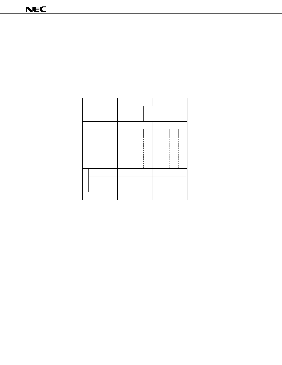
�
PD17704, 17705, 17707, 17708, 17709
54
5.8 Program Status Word (PSWORD)
5.8.1 Configuration of program status word
Figure 5-9 shows the configuration of the program status word.
As shown in the figure, th program status word consists of a total of 5 bits including the lowest bit of system
register address 7EH (RPL) and 4 bits of address 7FH (PSW).
Each bit of the program status word has its own function. The 5 bits of the program status word are BCD
flag (BCD), compare flag (CMP), carry flag (CY), zero flag (Z), and index enable flag (IXE).
Figure 5-9. Configuration of Program Status Word
7EH
RPL
0
0
0
Retained
7FH
PSW
0
0
0
Retained
b
3
b
2
b
1
b
0
B
C
D
b
3
C
M
P
b
2
C
Y
b
1
Z
b
0
I
X
E
Program status word
(PSWORD)
Address
Name
Symbol
Bit
Data
Clock stop
Power-ON reset
WDT&SP reset
CE reset
At reset
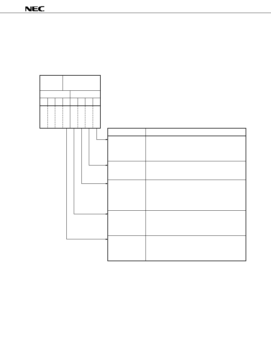
55
�
PD17704, 17705, 17707, 17708, 17709
5.8.2 Function of program status word
The program status word is a register that sets the conditions under which the ALU (Arithmetic Logic Unit)
executes an operation or data transfer, or indicates the result of an operation.
Table 5-2 outlines the function of each flag of the program status word.
For details, refer to 7. ALU (Arithmetic Logic Unit) BLOCK.
Table 5-2. Outline of Function of Each Flag of Program Status Word
5.8.3 Cautions on using program status word
When an arithmetic operation (addition or subtraction) is executed to the program status word, the "result"
of the arithmetic operation is stored.
For example, even if an operation that generates a carry is executed, if the result of the operation is 0000B,
0000B is stored to the PSW.
Program Status
Word (PSWORD)
RPL
PSW
b
3
b
2
b
1
b
0
B
C
D
b
3
C
M
P
b
2
C
Y
b
1
Z
b
0
I
X
E
Flag Name
Index enable flag
(IXE)
Zero flag
(Z)
Carry flag
(CY)
Compare flag
(CMP)
BCD flag
(BCD)
Function
Modifies address of data memory when data memory
manipulation instruction is exeuted.
0 : Does not modify
1 : Modifies
Indicates result of arithmetic operation is zero.
Status of this flag differs depending on contents of compare
flag.
Indicates occurrence of carry or borrow as result of execution
of addition or subtraction instruction.
This flag is reset to 0 if no carry or borrow occurs.
It is set to 1 if carry or borrow occurs.
This flag is also used as shift bit of "RORC r" instruction.
Indicates whether result of arithmetic operation is stored to
data memory or general register.
0 : Stores result.
1 : Does not store result.
Indicates whether arithmetic operation is performed in decimal
or binary.
0 : Binary operation
1 : Decimla operation
(RP)
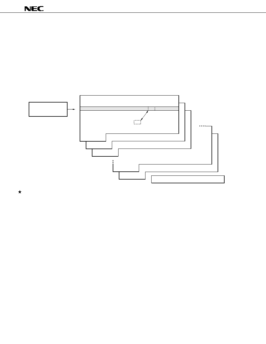
�
PD17704, 17705, 17707, 17708, 17709
56
6. GENERAL REGISTER (GR)
6.1 Outline of General Register
Figure 6-1 outlines the general register.
As shown in the figure, the general register is specified in the data memory by the general register pointer.
The bank and row address of the general register are specified by the general register pointer.
The general register is used to transfer or operate data between data memory addresses.
Figure 6-1. Outline of General Register
Remark
The
�
PD17704 and 17705 do not have BANKs 6 through 14.
The
�
PD17707 and 17708 do not have BANKs 10 through 14.
6.2 General Register
The general register consists of 16 nibbles (16
�
4 bis) of the same row address on the data memory.
For the range of the banks and row addresses that can be specified by the general register pointer as a general
register, refer to 5.7 General Register Pointer (RP).
The 16 nibbles of the same row address specified as a general register operate or transfer data with the data
memory by a single instruction.
In other words, operation or data transfer between data memory addresses can be executed by a single
instruction.
The general register can be controlled by the data memory manipulation instruction, like the other data
memory areas.
Column address
BANK2
BANK1
BANK0
Data memory
General register
Transfer, operation
General register
pointer
System register
BANK15
BANK14
Row address

57
�
PD17704, 17705, 17707, 17708, 17709
6.3 Generating Address of General Register by Each Instruction
The following sections 6.3.1 and 6.3.2 explain how the address of the general register is generated when each
instruction is executed.
For the details of the operation of each instruction, refer to 7. ALU (Arithmetic Logic Unit) BLOCK.
6.3.1 Add ("ADD r, m", "ADDC r, m") ,
subtract ("SUB r, m", "SUBC r, m") ,
logical operation ("AND r, m", "OR r, m", "XOR r, m"),
direct transfer ("LD r, m", "ST m, r"), and
rotation ("RORC r") instructions
Table 6-1 shows the address of the general register specified by operand "r" of an instruction. Operand "r"
of an instruction specifies only a column address.
Table 6-1. Generating Address of General Register
6.3.2 Indirect transfer ("MOV @r, m", "MOV m, @r") instruction
Table 6-2 shows a general register address specified by instruction operand "r" and an indirect transfer
address specified by "@r".
Table 6-2. Generating Address of General Register
6.4 Cautions on Using General Register
6.4.1 Row address of general register
Because the row address of the general register is specified by the general register pointer, the currently
specified bank may differ from the bank of the general register.
6.4.2 Operation between general register and immediate data
No instruction is available that executes an operation between the general register and immediate data.
To execute an operation between the general register and immediate data, the general register must be
treated as a data memory area.
General register address
Column address
Row address
Bank
b
3
b
2
b
1
b
0
b
2
b
1
b
0
b
3
b
2
b
1
b
0
r
Contents of general register pointer
General register address
Indirect transfer address
Column address
Row address
Bank
b
3
b
2
b
1
b
0
b
2
b
1
b
0
b
3
b
2
b
1
b
0
r
Contents of general register pointer
Contents of "r"
Same as data memory
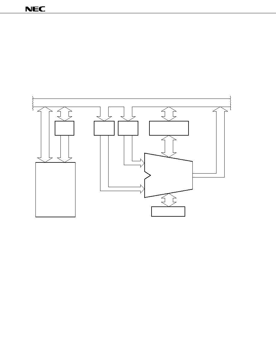
�
PD17704, 17705, 17707, 17708, 17709
58
7. ALU (Arithmetic Logic Unit) BLOCK
7.1 Outline of ALU Block
Figure 7-1 outlines the ALU block.
As shown in the figure, the ALU block consists of an ALU, temporary registers A and B, program status word,
decimal adjustment circuit, and memory address control circuit.
The ALU operates on, judges, compares, rotates, and transfers 4-bit data in the data memory.
Figure 7-1. Outline of ALU Block
Data bus
Address
control
Data memory
Index modification
memory pointer
Temporary
register A
Temporary
register B
Program status word
Carry/borrow/zero
detection/decimal/storage
specification
ALU
� Arithmetic operation
� Logical operation
� Bit judgment
� Comparison
� Rotation
� Transfer
Decimal adjustment

59
�
PD17704, 17705, 17707, 17708, 17709
7.2 Configuration and Function of Each Block
7.2.1 ALU
The ALU performs arithmetic operation, logical operation, bit judgment, comparison, rotation, and transfer
of 4-bit data according to instructions specified by the program.
7.2.2 Temporay registers A and B
Temporary registers A and B temporarily store 4-bit data.
These registers are automatically used when an instruction is executed, and cannot be controlled by program.
7.2.3 Program status word
The program status word controls the operation of and stores the status of the ALU.
For further information on the program status word, also refer to 5.8 Program Status Word (PSWORD).
7.2.4 Decimal adjustment circuit
The decimal adjustment circuit converts the result of an arithmetic operation into a decimal number if the BCD
flag of the program status word is set to "1" during arthmetic operations.
7.2.5 Address control circuit
The address control circuit specifies an address of the data memory.
At this time, address modification by the index register and data memory row address pointer is also
controlled.
7.3 ALU Processing Instruction List
Table 7-1 lists the ALU operations when each instruction is executed.
Table 7-2 shows how data memory addresses are modified by the index register and data memory row
address pointer.
Table 7-3 shows decimal adjustment data when a decimal operation is performed.
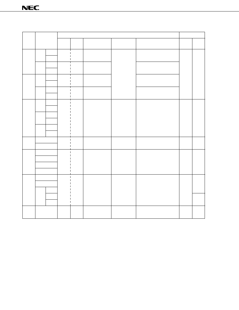
�
PD17704, 17705, 17707, 17708, 17709
60
Table 7-1. List of ALU Processing Instruction Operations
ALU
Instruction
Difference in Operation Depending on Program Status Word (PSWORD)
Address Modification
Function
Value of
Value of
Operation
Operation of
Operation of Z flag
Index
Memory
BCD flag CMP flag
CY flag
pointer
Add
ADD
r, m
0
0
Stores result of
Set if carry or
Set if result of operation
Modifies Does not
m, #n4
binary operation
borrow occurs;
is 0000B; otherwise, reset
modify
ADDC r, m
0
1
Does not store result otherwise, reset
Retains status if result of operation
m, #n4
of binary operation
is 0000B; otherwise, reset
Subtract SUB
r, m
1
0
Stores result of
Set if result of operation
m, #n4
decimal operation
is 0000B; otherwise, reset
SUBC r, m
1
1
Does not store result
Retains status if result of operation
m, #n4
of decimal operation
is 0000B; otherwise, reset
Logical
OR
r, m
Don't care Don't care Not affected
Retains previous Retains previous status
Modifies Does not
operation
m, #n4 (retained) (retained)
status
modify
AND
r, m
m, #n4
XOR
r, m
m, #n4
Judge
SKT
m, #n
Don't care Don't care Not affected
Retains previous Retains previous status
Modifies Does not
SKF
m, #n
(retained)
(reset)
status
modify
Compare SKE
m, #n4 Don't care Don't care Not affected
Retains previous Retains previous status
Modifies Does not
SKNE m, #n4 (retained) (retained)
status
modify
SKGE m, #n4
SKLT
m, #n4
Transfer LD
r, m
Don't care Don't care Not affected
Retains previous Retains previous status
Modifies Does not
ST
m, r
(retained) (retained)
status
modify
MOV
m, #n4
@r, m
Modifies
m, @r
Rotate
RORC r
Don't care Don't care Not affected
Value of b
0
of
Retains previous status
Does not Does not
(retained) (retained)
general register
modify
modify

61
�
PD17704, 17705, 17707, 17708, 17709
Table 7-2. Modification of Data Memory Address and Indirect Transfer Address by Index
Register and Data Memory Row Address Pointer
BANK
: bank register
IX
: index register
IXE
: index enable flag
IXH
: bits 10 through 8 of index register
IXM
: bits 7 through 4 of index register
IXL
: bits 3 through 0 of index register
m
: data memory address indicated by m
R
, m
C
m
R
: data memory row address (high-order)
m
C
: data memory column address (low-order)
MP
: data memory row address pointer
MPE : memory pointer enable flag
r
: general register column address
RP
: general register pointer
(X)
: contents addressed by X
X: direct address such as "m" and "r"
b
3
b
2
b
1
b
0
b
2
b
1
b
0
b
3
b
2
b
1
b
0
b
3
b
2
b
1
b
0
b
2
b
1
b
0
b
3
b
2
b
1
b
0
b
3
b
2
b
1
b
0
b
2
b
1
b
0
b
3
b
2
b
1
b
0
General Register Address Specified by "r"
Data Memory Address Specified by "m"
Indirect Transfer Address Specified by "@r"
Bank
Row
address
Column
address
Bank
Row
address
Column
address
Bank
Row
address
Column
address
RP
r
BANK
m
BANK
m
R
(r)
ditto
MP
(r)
ditto
BANK
m
BANK
m
R
IX
(r)
OR
MP
(r)
ditto
ditto
ditto
MPE
0
1
0
1
IXE
0
0
1
1
IXH, IXM
Logical
OR
Logical
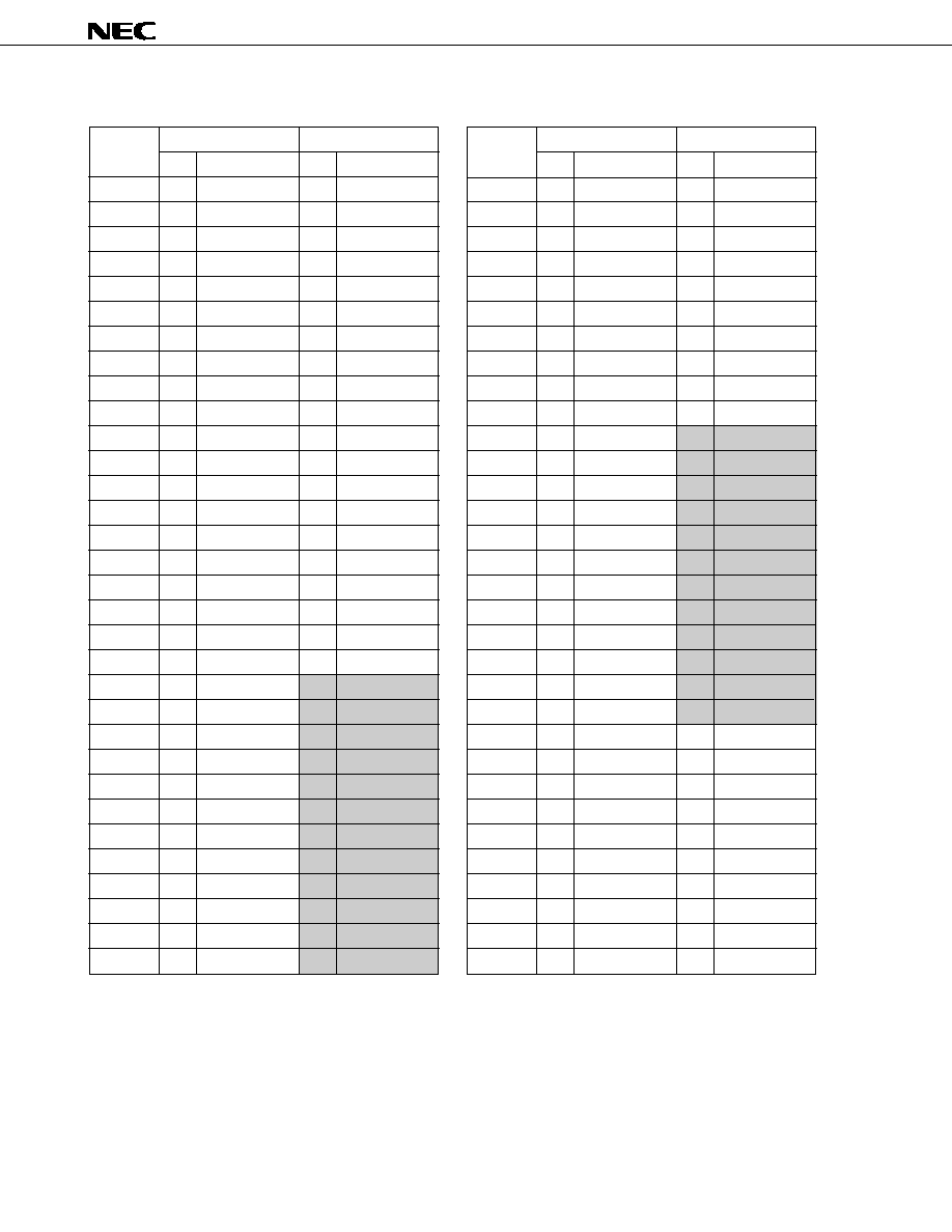
�
PD17704, 17705, 17707, 17708, 17709
62
Table 7-3. Decimal Adjustment Data
Operation Hexadecimal Addition
Decimal Addition
Operation Hexadecimal Addition
Decimal Addition
Result
CY
Operation result
CY
Operation result
Result
CY
Operation result
CY
Operation result
0
0
0000B
0
0000B
0
0
0000B
0
0000B
1
0
0001B
0
0001B
1
0
0001B
0
0001B
2
0
0010B
0
0010B
2
0
0010B
0
0010B
3
0
0011B
0
0011B
3
0
0011B
0
0011B
4
0
0100B
0
0100B
4
0
0100B
0
0100B
5
0
0101B
0
0101B
5
0
0101B
0
0101B
6
0
0110B
0
0110B
6
0
0110B
0
0110B
7
0
0111B
0
0111B
7
0
0111B
0
0111B
8
0
1000B
0
1000B
8
0
1000B
0
1000B
9
0
1001B
0
1001B
9
0
1001B
0
1001B
10
0
1010B
1
0000B
10
0
1010B
1
1100B
11
0
1011B
1
0001B
11
0
1011B
1
1101B
12
0
1100B
1
0010B
12
0
1100B
1
1110B
13
0
1101B
1
0011B
13
0
1101B
1
1111B
14
0
1110B
1
0100B
14
0
1110B
1
1100B
15
0
1111B
1
0101B
15
0
1111B
1
1101B
16
1
0000B
1
0110B
�16
1
0000B
1
1110B
17
1
0001B
1
0111B
�15
1
0001B
1
1111B
18
1
0010B
1
1000B
�14
1
0010B
1
1100B
19
1
0011B
1
1001B
�13
1
0011B
1
1101B
20
1
0100B
1
1110B
�12
1
0100B
1
1110B
21
1
0101B
1
1111B
�11
1
0101B
1
1111B
22
1
0110B
1
1100B
�10
1
0110B
1
0000B
23
1
0111B
1
1101B
�9
1
0111B
1
0001B
24
1
1000B
1
1110B
�8
1
1000B
1
0010B
25
1
1001B
1
1111B
�7
1
1001B
1
0011B
26
1
1010B
1
1100B
�6
1
1010B
1
0100B
27
1
1011B
1
1101B
�5
1
1011B
1
0101B
28
1
1100B
1
1010B
�4
1
1100B
1
0110B
29
1
1101B
1
1011B
�3
1
1101B
1
0111B
30
1
1110B
1
1100B
�2
1
1110B
1
1000B
31
1
1111B
1
1101B
�1
1
1111B
1
1001B
Remark
Decimal adjustment is not correctly carried out in the shaded area in the above table.

63
�
PD17704, 17705, 17707, 17708, 17709
7.4 Cautions on Using ALU
7.4.1 Cautions on execution operation to program status word
If an arithmetic operation is executed to the program status word, the result of the operation is stored to the
program status word.
The CY and Z flags in the program status word are usually set or reset by the result of the arithmetic operation.
If an arithmetic operation is executed to the program status word itself, the result of the operation is stored to
the program status word, and consequently, it cannot be judged whether a carry or borrow occurs or whether
the result of the operation is zero.
If the CMP flag is set, however, the result of the operation is not stored to the program status word. Therefore,
the CY and Z flags are set or reset normally.
7.4.2 Cautions on executing decimal operation
The decimal operation can be executed only when the result of the operation falls within the following ranges:
(1) Result of addition
: 0 to 19 in decimal
(2) Result of subtraction: 0 to 9 or �10 to �1 in decimal
If a decimal operation is executed exceeding or falling below the above ranges, the result is a value greater
than 1010B (0AH).
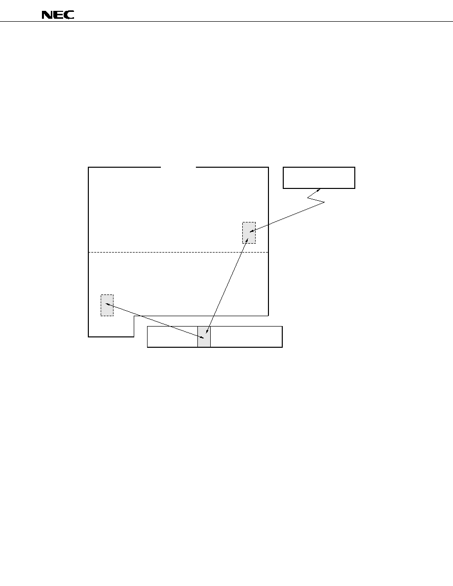
�
PD17704, 17705, 17707, 17708, 17709
64
8. REGISTER FILE (RF)
8.1 Outline of Register File
Figure 8-1 outlines the register file.
As shown in the figure, the rgister file consists of the control registers existing on a space different from the
data memory, and a portion overlapping the data memory.
The control registers set conditions of the peripheral hardware units.
The data on the register file can be read or written via window register.
Figure 8-1. Outline of Register File
Control register
(on separate space from data memory)
(Same space as data memory)
Data manipulation via window register
0
1
2
3
4
5
6
7
System register
Window register
Peripheral hardware
Register file
Row address
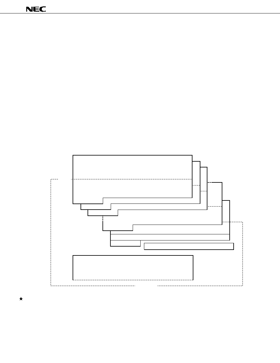
65
�
PD17704, 17705, 17707, 17708, 17709
8.2 Configuration and Function of Register File
Figure 8-2 shows the configuration of the register file and the relationships between the register file and data
memory.
The register file is assigned addresses in 4-bit units, like the data memory, and consists of a total of 128
nibbles with row addresses 0H through 7FH and column addresses 0H through 0FH.
Addresses 00H through 3FH are control registers that sets the conditions of the peripheral hardware units.
Addresses 40H through 7FH overlap the data memory.
In other words, addresses 40H through 7FH of the register file are addresses 40H through 7FH of the
currently-selected bank of data memory.
Because addresses 40H through 7FH of the register file overlap the same addresses of the data memory,
these addresses of the register file can be manipulated in the same manner as the data memory, except that
the addresses of the register file can also be manipulated by using register file manipulation instructions ("PEEK
WR, rf" and "POKE rf, WR"). Note, however, that addresses 60H through 6FH of BANK15 are assigned port
input/output selection registers (for details refer to 8.4 Port Input/Output Selection Registers).
Figure 8-2. Configuration of Register File and Relationship with Data Memory
Remark
The
�
PD17704 and 17705 do not have BANKs 6 through 14.
The
�
PD17707 and 17708 do not have BANKs 10 through 14.
Column address
0
1
2
3
4
5
6
7
0
1
2
3
4
5
6
7
8
9
A
B
C
D
E
F
System registers
0
1
2
3
Control registers
Data memory
BANK0
BANK1
BANK2
BANK14
Register file
BANK15
Port input/output selection registers
Row address

�
PD17704, 17705, 17707, 17708, 17709
66
8.2.1 Register file manipulation instructions ("PEEK WR, rf", "POKE rf, WR")
Data is read from or written to the register file via the window register of the system registers, by using the
following instructions.
(1) "PEEK WR, rf"
Reads data of the register file addressed by "rf" to the window register.
(2) "POKE rf, WR"
Writes the data of the window register to the register file addressed by "rf".
8.3 Control Registers
Figure 8-3 shows the configuration of the control registers.
As shown in the figure, the control registers consist of a total of 64 nibbles (64
�
4 bits) of addresses 00H
through 3FH of the register file.
Of these 64 nibbles, however, only 53 nibbles are actually used. The remaining 11 nibbles are unused
registers and prohibited from being written or read.
Each control register has an attribute of 1 nibble that identifies four types of registers: read/write (R/W), read-
only (R), write-only (W), and read-and-reset (R&Reset) registers.
Nothing is changed even if data is written to a read-only (R and R&Reset) register.
An "undefined" value is read if a write-only (W) register is read.
Among the 4-bit data in 1 nibble, the bit fixed to "0" is always "0" when it is read, and is also "0" when it is
written.
The 11 nibbles of unused registers are undefined when their contents are read, and nothing changes even
when they are written.
Table 8-1 lists the peripheral hardware control functions of the control registers.

67
�
PD17704, 17705, 17707, 17708, 17709
[MEMO]

�
PD17704, 17705, 17707, 17708, 17709
68
Figure 8-3. Configuration of Control Registers (1/2)
Note
( ) indicates an address that is used when the assembler is used.
( )
( )
S
P
3
S
P
2
( )
S
P
1
( )
S
P
0
0
0 W
D
T
C
K
1
W
D
T
C
K
0
W
D
T
R
E
S
0
0
0
0
0
( )
D
B
F
S
P
1
( )
D
B
F
S
P
0
0
0
I
S
P
R
E
S
A
S
P
R
E
S
C
E
C
N
T
3
C
E
C
N
T
2
C
E
C
N
T
1
C
E
C
N
T
0
0
0 M
O
V
T
S
E
L
1
M
O
V
T
S
E
L
0
P
L
L
R
F
C
K
3
P
L
L
R
F
C
K
2
P
L
L
R
F
C
K
1
P
L
L
R
F
C
K
0
0
0
0
P
L
L
U
L
0
0
B
E
E
P
1
S
E
L
B
E
E
P
0
S
E
L
B
E
E
P
1
C
K
1
B
E
E
P
1
C
K
0
B
E
E
P
0
C
K
1
B
E
E
P
0
C
K
0
0
0
0 W
D
T
C
Y
0
0
0
B
T
M
0
C
Y
P
L
L
S
C
N
F
0
P
L
L
M
D
1
P
L
L
M
D
0
0
0
0
I
F
C
G
O
S
T
T
I
F
C
M
D
1
I
F
C
M
D
0
I
F
C
C
K
1
I
F
C
C
K
0
0
0
I
F
C
S
T
R
T
I
F
C
R
E
S
0
A
D
C
C
H
2
A
D
C
C
H
1
A
D
C
C
H
0
0
A
D
C
M
D
A
D
C
S
T
T
A
D
C
C
M
P
0
P
W
M
B
I
T
0
P
W
M
C
K
0
P
W
M
2
S
E
L
P
W
M
1
S
E
L
P
W
M
0
S
E
L
0
0
F
C
G
C
H
1
F
C
G
C
H
0
0
0
0
I
R
Q
S
I
O
1
0
0
0
I
R
Q
S
I
O
0
0
0
0
I
R
Q
T
M
3
0
0
0
I
R
Q
T
M
2
0
1
2
3
4
5
6
7
R/W
R/W
W & Reset
R
R/W
R/W
R/W
Read/
Write
R/W
R/W
R&Reset
R/W
R/W
R&Reset
R&Reset
Read/
Write
R/W
R
R/W
W
R/W
R/W
R/W
R/W
Read/
Write
R
R/W
R/W
R/W
R/W
Read/
Write
Column Address
Row
Address
Item
Name Stack
pointer
Watchdog
timer clock
selection
Watchdog
timer counter
reset
Data buffer
stack pointer
Stack overflow/
underflow reset
selection
CE reset
timer carry
counter
MOVT bit
selection
Symbol
Name PLL
mode
selection
PLL reference
frequency
selection
PLL unlock
FF
BEEP/general
-purpose port
pin function
selection
BEEP clock
selection
Watchdog
timer/stack
pointer reset
status detection
Basic timer
0 carry
Name FCG
channel
selection
IF counter
gate status
detection
IF counter
mode
selection
IF counter
control
A/D converter
channel
selection
PWM clock
selection
PWM/general-
purpose port
pin function
selection
A/D converter
mode
selection
Symbol
Name Serial
interface 1
interrupt
request
Timer 3
interrupt
request
Serial
interface 0
interrupt
request
Symbol
Timer 2
interrupt
request
0
1
2
3
(8)
Note
(9)
Note
(A)
Note
(B)
Note
Symbol
69
�
PD17704, 17705, 17707, 17708, 17709
Figure 8-3. Configuration of Control Register (2/2)
S
I
O
0
I
M
D
1
S
I
O
0
I
M
D
0
0
0
0
S
I
O
0
W
S
T
T
0
S
B
M
D
S
I
O
0
C
K
1
S
I
O
0
C
K
0
0
0
( )
( )
S
I
O
0
S
F
8
S
I
O
0
S
F
9
S
B
S
T
T
S
B
B
S
Y
S
B
A
C
K
S
I
O
0
N
W
T
S
I
O
0
W
R
Q
1
S
I
O
0
W
R
Q
0
S
I
O
0
C
H
S
B
S
I
O
0
M
S
S
I
O
0
T
X
S
I
O
1
T
S
S
I
O
1
H
I
Z
S
I
O
1
C
K
1
S
I
O
1
C
K
0
I
E
G
4
I
N
T
4
S
E
L
I
E
G
3
I
N
T
3
S
E
L
0
I
E
G
2
I
E
G
1
I
E
G
0
0
0
B
T
M
0
C
K
1
B
T
M
0
C
K
0
T
M
2
E
N
T
M
2
R
E
S
T
M
2
C
K
1
T
M
2
C
K
0
T
M
1
E
N
T
M
1
R
E
S
T
M
1
C
K
1
T
M
1
C
K
0
T
M
0
E
N
T
M
0
R
E
S
T
M
0
C
K
1
T
M
0
C
K
0
T
M
0
O
V
F
T
M
0
G
C
E
G
T
M
0
G
O
E
G
T
M
0
M
D
I
P
S
I
O
1
I
P
S
I
O
0
I
P
T
M
3
I
P
T
M
2
I
P
T
M
1
I
P
T
M
0
I
P
4
I
P
3
I
P
2
I
P
1
I
P
0
I
P
C
E
T
M
3
S
E
L
0
T
M
3
E
N
T
M
3
R
E
S
8
9
A
B
C
D
E
F
R
R
R/W
R/W
R
R/W
R/W
R/W
R/W
R/W
R/W
R/W
R/W
R/W
R/W
R/W
R/W
R/W
R/W
System register
interrupt stack
pointer
Serial I/O0
wait status
judgment
Serial I/O0
clock
selection
Serial I/O0
interrupt mode
selection
Serial I/O0
status
detection
Serial I/O0
wait control
Serial I/O0
mode
selection
Basic timer 0
clock
selection
Interrupt
edge
selection 1
Timer 3
control
Timer 2
counter clock
selection
Timer 1
counter clock
selection
Timer 0
counter clock
selection
Timer 0
mode
selection
Interrupt
enable 2
Interrupt
enable 1
INT2 pin
interrupt
request
INT0 pin
interrupt
request
CE pin
interrupt
request
0
S
Y
S
R
S
P
2
S
Y
S
R
S
P
1
S
Y
S
R
S
P
0
( )
Serial I/O1
mode
selection
Interrupt
edge
selection 2
Interrupt
enable 3
0
0
0
I
N
T
4
0
0
I
R
Q
4
I
N
T
3
0
0
I
R
Q
3
I
N
T
2
0
0
I
R
Q
2
I
N
T
1
0
0
I
R
Q
1
I
N
T
0
0
0
I
R
Q
0
C
E
0
C
E
C
N
T
S
T
T
I
R
Q
C
E
0
0
0
I
R
Q
T
M
1
R/W
R/W
R/W
R/W
R/W
R/W
R/W
R
I
R
Q
T
M
0
R
/
W
Timer 1
interrupt
request
Timer 0
interrupt
request
INT4 pin
interrupt
request
INT3 pin
interrupt
request
INT1 pin
interrupt
request

�
PD17704, 17705, 17707, 17708, 17709
70
Table 8-1. Peripheral Hardware Control Functions of Control Registers (1/8)
Peripheral
Control Register
Peripheral Hardware Control Function
At Reset
Clock
Hardware
Name
Address
Read/
Function
Set value
Power- WDT
CE
Stop
Write
Symbol
ON
& SP
reset
0
1
reset
reset
Stack
Stack pointer
01H
R/W
(SP3)
F
F
F
Retained
(SP2)
(SP1)
(SP0)
Interrupt stack
08H
R
0
5
5
5
Retained
pointer of
(SYSRSP2)
system register
(SYSRSP1)
(SYSRSP0)
Data buffer
04H
R
0
Fixed to "0"
0
0
0
Retained
stack pointer
0
(DBFSP1)
Detects nesting level
(DBFSP0)
of data buffer stack
Stack overflow/
05H
R/W
0
Fixed to "0"
3
Retained Retained Retained
underflow reset
0
selection
ISPRES
Selects interrupt stack
Reset
Reset valid
overflow/underflow reset
prohibited
(can be set only once
following power application)
ASPRES
Selects address stack
overflow/underflow reset
(can be set only once
following power application)
Watchdog Watchdog timer
02H
R/W
0
Fixed to "0"
3
Retained Retained Retained
timer
clock selection
0
WDTCK1
Selects clock of watchdog timer (can be
WDTCK0
set only once following power application)
Watchdog timer
03H
W &
WDTRES
Resets watchdog timer counter
Invalid
Reset if written
Undefined Undefined Undefined Undefined
counter reset
Reset 0
Fixed to "0"
0
0
WDT&SP reset
16H
R &
0
0
1
Retained Retained
status detection
Reset 0
0
WDTCY
Detects resetting of watchdog
No reset
Reset request
timer/stack pointer
request
b
3
b
2
b
1
b
0
0
0
1
1
Level 0
Level 1
Level 2
Level 3
0
1
0
1
0
0
1
1
Not 65536
Setting
131072
used instruction prohibited instruction
0
1
0
1

71
�
PD17704, 17705, 17707, 17708, 17709
Table 8-1. Peripheral Hardware Control Functions of Control Registers (2/8)
Peripheral
Control Register
Peripheral Hardware Control Function
At Reset
Clock
Hardware
Name
Address
Read/
Function
Set value
Power- WDT
CE
Stop
Write
Symbol
ON
& SP
reset
0
1
reset
reset
CE
CE reset timer
06H
R/W
CECNT3
Sets number of CE reset timer
1
Retained Retained
1
carry counter
CECNT2
carry counts
CECNT1
CECNT0
MOVT bit
07H
R/W
0
Fixed to "0"
0
0
0
Retained
selection
0
MOVTSEL1
Sets bit transferred by MOVT (transferred
MOVTSEL0
to DBF1, 0 during 8-bit transfer)
Serial
Serial I/O0 wait
0AH
R
0
Fixed to "0"
0
0
0
0
interface status judgment
0
0
SIO0WSTT Judges wait status of serial
During wait
During serial
interface 0
communication
Serial I/O0
0BH
R/W
0
Fixed to "0"
0
0
0
0
clock selection
SBMD
Selects operation mode of I
2
C
Continues
Reception mode is
bus during slave transmission
processing
set automatically
SIO0CK1
Sets internal clck of serial
SIO0CK0
interface 0
Serial I/O0
0CH
R/W
0
Fixed to "0"
0
0
0
0
interrupt mode
0
selection
SIO0IMD1
Sets interrupt condition of
SIO0IMD0
serial interface 0
Serial I/O0
0DH
R
SIO0SF8
Detects clock counter
Set at 8th clock
0
0
0
0
status detection
SIO0SF9
Set at 9th clock
SBSTT
Detects number of clocks
Set from start condition to
(I
2
C bus mode)
9th clock
SBBSY
Detects start condition
Set from start condition to
(I
2
C bus mode)
stop condition
Serial I/O0 wait
0EH
R/W
SBACK
Sets and detects acknowledge Sets and detects 0, 1
0
0
0
0
control
(I
2
C bus mode)
SIO0NWT
Enables wait
Enabled
Cleared
SIO0WRQ1 Sets wait mode
SIO0WRQ0
0: Setting prohibited
1: 1 count
2: 2 counts 3: 3 counts 4: 4 counts
5: 5 counts 6: 6 counts 7: 7 counts
8: 8 counts 9: 9 counts A: 10 counts
B: 11 counts C: 12 counts D: 13 counts
E: 14 counts F: 15 coounts
00
0
1
16-bit
High-order
Low-order
transfer 8-bit transfer 8-bit transfer
01
1
0
0
0
1
1
93.75
375
281.25
46.875
kHz
kHz
kHz
kHz
0
1
0
1
0
0
1
1
7th
8th
7th clock
Stop
clock
clock
after start
condition
condition
0
1
0
1
0
0
1
1
No
Data
Acknowledge
Address
wait
wait
wait
wait
0
1
0
1
b
3
b
2
b
1
b
0
�
PD17704, 17705, 17707, 17708, 17709
72
Table 8-1. Peripheral Hardware Control Functions of Control Registers (3/8)
Peripheral
Control Register
Peripheral Hardware Control Function
At Reset
Clock
Hardware
Name
Address
Read/
Function
Set value
Power- WDT
CE
Stop
Write
Symbol
ON
& SP
reset
0
1
reset
reset
Serial
Serial I/O0
0FH
R/W
SIO0CH
Selects serial I/O0 mode
0
0
0
0
interface mode selection
SB
SIO0MS
Sets master/slave
Slave operation
Master operation
SIO0TX
Sets transfer direction
Reception
Transmission
Serial I/O1
1DH
R/W
SIO1TS
Starts or stops operation
Stops operation Starts operation
0
0
0
0
mode selection
SIO1HIZ
Sets status of P0B1/SO1 pin
General-purpose
Serial data
I/O port
output pin
SIO1CK1
Sets I/O clock
SIO1CK0
PLL
PLL mode
10H
R/W
PLLSCNF
Sets low-order bits of swallow counter
Lowest bit is 0 Lowest bit is 1
U
U
R
R
frequency
selection
0
Fixed to "0"
0
0
0
0
synthesizer
PLLMD1
Sets division mode of PLL
PLLMD0
PLL reference
11H
R/W
PLLRFCK3
Sets reference frequency of PLL
F
F
F
F
frequency
PLLRFCK2
selection
PLLRFCK1
PLLRFCK0
PLL unlcok FF
12H
R &
0
Fixed to "0"
Undefined Undefined
Retained Retained
Reset 0
0
PLLUL
Detects status of unlock FF
Locked
Unclocked
BEEP
BEEP/general-
13H
R/W
0
Fixed to "0"
0
0
0
0
purpose port pin
0
function selection
BEEP1SEL Selects function of P1D1/BEEP1 pin General-purpose
BEEP
BEEP0SEL Selects function of P1D0/BEEP0 pin
I/O port
BEEP clock
14H
R/W
BEEP1CK1 Sets output frequency of BEEP1
0
0
0
0
selection
BEEP1CK0
BEEP0CK1 Sets output frequency of BEEP0
BEEP0CK0
U: Undefined R: Retained
0
0
1
1
Not
I
2
C
2-wire
3-wire
used
mode
mode
mode
0
1
0
1
0: 1.25 kHz 1: 2.5 kHz
2: 5 kHz
3: 10 kHz
4: 6.25 kHz 5: 12.5 kHz
6: 25 kHz
7: 50 kHz
8: 3 kHz
9: 9 kHz
A: 18 kHz
B: Setting prohibited
C: 1 kHz
D: 20 kHz
E: Setting prohibited
F: PLL disabled
0
0
1
1
Disabled
MF
VHF
HF
0
1
0
1
0
0
1
1
4 kHz
3 kHz
200 Hz
67 Hz
0
1
0
1
0
0
1
1
1 kHz
3 kHz
4 kHz
6.7 kHz
0
1
0
1
0
0
1
1
External 187.50
375.00
46.875
clock
kHz
kHz
kHz
0
1
0
1
b
3
b
2
b
1
b
0

73
�
PD17704, 17705, 17707, 17708, 17709
Table 8-1. Peripheral Hardware Control Functions of Control Registers (4/8)
Peripheral
Control Register
Peripheral Hardware Control Function
At Reset
Clock
Hardware
Name
Address
Read/
Function
Set value
Power- WDT
CE
Stop
Write
Symbol
ON
& SP
reset
0
1
reset
reset
Timer
Basic timer
17H
R &
0
Fixed to "0"
0
Retained
1
Retained
0 carry
Reset 0
0
BTM0CY
Detects basic timer 0 carry FF
FF reset
FF set
Basic timer 0
18H
R/W
0
Fixed to "0"
0
0
Retained Retained
clock selection
0
BTM0CK1
Selects clock of basic timer 0
BTM0CK0
Timer 3 control
28H
R/W
TM3SEL
Selects timer 3 and D/A converter D/A converter
Timer 3
0
0
Retained
0
0
Fixed to "0"
TM3EN
Starts or stops timer 3 counter
Stops
Starts
TM3RES
Resets timer 3 counter
Not affected
Reset
Timer 2 counter
29H
R/W
TM2EN
Starts or stops timer 2 counter
Stops
Starts
0
0
Retained
0
clock selection
TM2RES
Resets timer 2 counter
Not affected
Reset
TM2CK1
Sets basic clock of timer
TM2CK0
2 counter
Timer 1 counter
2AH
R/W
TM1EN
Starts or stops timer 1 counter
Stops
Starts
0
0
Retained
0
clock selection
TM1RES
Resets timer 1 counter
Not affected
Reset
TM1CK1
Sets basic clock of timer
TM1CK0
1 counter
Timer 0 counter
2BH
R/W
TM0EN
Starts or stops timer 0 counter
Stops
Starts
0
0
Retained
0
clock selection
TM0RES
Resets timer 0 counter
Not affected
Reset
TM0CK1
Sets basic clock of timer
TM0CK0
0 counter
Timer 0 mode
2CH
R/W
TM0OVF
Detects timer 0 overflow
No overflow
Overflow
0
0
Retained
0
selection
TM0GCEG
Sets edge of gate close input
Rising edge
Falling edge
signal
TM0GOEG
Sets edge of gate open input
signal
TM0MD
Selects modulo counter/gate
Modulo counter Gate counter
counter of timer 0
0
0
1
1
10 Hz
20 Hz
50 Hz
100 Hz
0
1
0
1
0
0
1
1
100 kHz 10 kHz
2 kHz
1 kHz
0
1
0
1
0
0
1
1
100 kHz 10 kHz
2 kHz
1 kHz
0
1
0
1
0
0
1
1
100 kHz 10 kHz
2 kHz
1 kHz
0
1
0
1
b
3
b
2
b
1
b
0

�
PD17704, 17705, 17707, 17708, 17709
74
Table 8-1. Peripheral Hardware Control Functions of Control Registers (5/8)
Peripheral
Control Register
Peripheral Hardware Control Function
At Reset
Clock
Hardware
Name
Address
Read/
Function
Set value
Power- WDT
CE
Stop
Write
Symbol
ON
& SP
reset
0
1
reset
reset
Interrupt Interrupt edge
1EH
R/W
IEG4
Sets interrupt issuance edge
Rising edge
Falling edge
0
0
Retained Retained
selection 1
(INT4 pin)
INT4SEL
Sets interrupt request flag of
Enables
Disables
P1A3/INT4 pin
setting of flag setting of flag
IEG3
Sets interrupt issuance edge
Rising edge
Falling edge
(INT3 pin)
INT3SEL
Sets interrupt request flag of
Enables
Disables
P1A2/INT3 pin
setting of flag setting of flag
Interrupt edge
1FH
R/W
0
Fixed to "0"
0
0
Retained Retained
selection 2
IEG2
Sets interrupt issuance edge
Rising edge
Falling edge
(INT2 pin)
IEG1
Sets interrupt issuance edge
(INT1 pin)
IEG0
Sets interrupt issuance edge
(INT0 pin)
Interrupt enable 1
2DH
R/W
IPSIO1
Enables serial interface 1
Disables
Enables
0
0
Retained Retained
interrupt
interrupt
interrupt
IPSIO0
Enables serial interface 0
interrupt
IPTM3
Enables timer 3 interrupt
IPTM2
Enables timer 2 interrupt
Interrupt enable 2
2EH
R/W
IPTM1
Enables timer 1 interrupt
Disables
Enables
0
0
Retained Retained
IPTM0
Enables timer 0 interrupt
interrupt
interrupt
IP4
Enables INT4 pin interrupt
IP3
Enables INT3 pin interrupt
Interrupt enable 3
2FH
R/W
IP2
Enables INT2 pin interrupt
Disables
Enables
0
0
Retained Retained
IP1
Enables INT1 pin interrupt
interrupt
interrupt
IP0
Enables INT0 pin interrupt
IPCE
Enables CE pin interrupt
Serial interface 1 34H
R/W
0
Fixed to "0"
0
0
Retained Retained
interrupt request
0
0
IRQSIO1
Detects serial interface 1
No interrupt
Interrupt
interrupt request
request
request
b
3
b
2
b
1
b
0

75
�
PD17704, 17705, 17707, 17708, 17709
Table 8-1. Peripheral Hardware Control Functions of Control Registers (6/8)
Peripheral
Control Register
Peripheral Hardware Control Function
At Reset
Clock
Hardware
Name
Address
Read/
Function
Set value
Power- WDT
CE
Stop
Write
Symbol
ON
& SP
reset
0
1
reset
reset
Interrupt Serial interface 0
35H
R/W
0
Fixed to "0"
0
0
Retained Retained
interrupt request
0
0
IRQSIO0
Detects serial interface 0
No interrupt request
Interrupt request
interrupt request
Timer 3 interrupt
36H
R/W
0
Fixed to "0"
0
0
Retained Retained
request
0
0
IRQTM3
Detects timer 3 interrupt request
No interrupt request
Interrupt request
Timer 2 interrupt
37H
R/W
0
Fixed to "0"
0
0
Retained Retained
request
0
0
IRQTM2
Detects timer 2 interrupt request
No interrupt request
Interrupt request
Timer 1 interrupt
38H
R/W
0
Fixed to "0"
0
0
Retained Retained
request
0
0
IRQTM1
Detects timer 1 interrupt request
No interrupt request
Interrupt request
Timer 0 interrupt
39H
R/W
0
Fixed to "0"
0
0
Retained Retained
request
0
0
IRQTM0
Detects timer 0 interrupt request
No interrupt request
Interrupt request
INT4 pin interrupt
3AH
R/W
INT4
Detects INT4 pin status
Low level
High level
U
U
U
U
request
0
Fixed to "0"
0
0
Retained Retained
0
IRQ4
Detects INT4 pin interrupt request
No interrupt request
Interrupt request
INT3 pin interrupt
3BH
R/W
INT3
Detects INT3 pin status
Low level
High level
U
U
U
U
request
0
Fixed to "0"
0
0
Retained Retained
0
IRQ3
Detects INT3 pin interrupt request
No interrupt request
Interrupt request
INT2 pin interrupt
3CH
R/W
INT2
Detects INT2 pin status
Low level
High level
U
U
U
U
request
0
Fixed to "0"
0
0
Retained Retained
0
IRQ2
Detects INT2 pin interrupt request
No interrupt request
Interrupt request
INT1 pin interrupt
3DH
R/W
INT1
Detects INT1 pin status
Low level
High level
U
U
U
U
request
0
Fixed to "0"
0
0
Retained Retained
0
IRQ1
Detects INT1 pin interrupt request
No interrupt request
Interrupt request
U: Undefined
b
3
b
2
b
1
b
0

�
PD17704, 17705, 17707, 17708, 17709
76
Table 8-1. Peripheral Hardware Control Functions of Control Registers (7/8)
Peripheral
Control Register
Peripheral Hardware Control Function
At Reset
Clock
Hardware
Name
Address
Read/
Function
Set value
Power- WDT
CE
Stop
Write
Symbol
ON
& SP
reset
0
1
reset
reset
Interrupt INT0 pin interrupt
3EH
R/W
INT0
Detects INT0 pin status
Low level
High level
U
U
U
U
request
0
Fixed to "0"
0
0
Retained Retained
0
IRQ0
Detects INT0 pin interrupt request
No interrupt request
Interrupt request
CE pin interrupt
3FH
R
CE
Detects CE pin status
Low level
High level
U
U
U
U
request
0
Fixed to "0"
0
0
0
0
CECNTSTT Detects CE reset counter status
Stops
Operates
R/W
IRQCE
Detects CE pin interrupt request
No interrupt request
Interrupt request
0
0
R
R
IF
FCG channel
20H
R/W
0
Fixed to "0"
0
0
0
0
counter
selection
0
FCGCH1
Sets pin to be used as FCG
FCGCH0
IF counter gate
21H
R
0
Fixed to "0"
0
0
0
0
status detection
0
0
IFCGOSTT
Detects IF counter gate status
Closed
Open
IF counter
22H
R/W
IFCMD1
Sets IF counter mode
0
0
0
0
mode selection
IFCMD0
IFCCK1
Sets IF counter gate time and
IFCCK0
FCG count frequency
IF counter
23H
W
0
Fixed to "0"
0
0
0
0
control
0
IFCSTRT
Starts or stops IF counter
Nothing affected Starts counter
IFCRES
Resets IF counter data
Nothing affected Starts counter
A/D
A/D converter
24H
R/W
0
Fixed to "0"
0
0
Retained Retained
converter channel
ADCCH2
Selects pin used for A/D converter
selection
ADCCH1
ADCCH0
A/D converter
25H
R/W
0
Fixed to "0"
0
0
0
0
mode selection
ADCMD
Selects comparison mode of
Software mode Hardware mode
Retained Retained
A/D converter
R
ADCSTT
Detects operating status of
Conversion ends
Converting
0
0
A/D converter
ADCCMP
Detects comparison result of
V
ADCREF
> V
ADCIN
V
ADCREF
< V
ADCIN
0
Retained
A/D converter
U: Undefined R: Retained
0
0
1
1
FCG
FCG0 FCG1 Setting
not used
pin
pin
prohibited
0
1
0
1
0
0
1
1
FCG
AMIFC
FMIFC
AMIFC2
0
1
0
1
0
0
1
1
1ms,
4 ms,
8 ms,
Open,
1 kHz 100 kHz 900 kHz Setting
prohibited
0
1
0
1
0: A/D converter not used
1: P0D0/AD0 pin
2: P0D1/AD1pin
3: P0D2/AD2 pin
4: P0D3/AD3 pin
5: P1C2/AD4 pin
6: P1C3/AD5 pin
7: Setting prohibited
b
3
b
2
b
1
b
0

77
�
PD17704, 17705, 17707, 17708, 17709
Table 8-1. Peripheral Hardware Control Functions of Control Registers (8/8)
Peripheral
Control Register
Peripheral Hardware Control Function
At Reset
Clock
Hardware
Name
Address
Read/
Function
Set value
Power- WDT
CE
Stop
Write
Symbol
ON
& SP
reset
0
1
reset
reset
D/A
PWM clock
26H
R/W
0
Fixed to "0"
0
0
Retained
0
converter selection
PWMBIT
Selects number of bits of PWM
8 bits
9 bits
counter
0
Fixed to "0"
PWMCK
Selects output clock of timer 3
4.4 kHz (8)/
440 Hz (8)/
2.2 kHz (9)
220 Hz (9)
PWM/general-
27H
R/W
0
Fixed to "0"
0
0
Retained
0
purpose port pin
PWM2SEL
Selects function of P1B2/PWM2 pin General-purpose D/A converter
function selection
PWM1SEL
Selects function of P1B1/PWM1 pin
output port
PWM0SEL
Selects function of P1B0/PWM0 pin
b
3
b
2
b
1
b
0

�
PD17704, 17705, 17707, 17708, 17709
78
8.4 Port Input/Output Selection Registers
Figure 8-4 shows the configuration of the port input/output selection registers.
As shown in this figure, the port input/output select registers consist of a total of 16 nibbles (16
�
4 bits) at
addresses 60H through 6FH of BANK 15 of the data memory.
Table 8-2 lists the control functions of the port input/output selection registers.

79
�
PD17704, 17705, 17707, 17708, 17709
[MEMO]

�
PD17704, 17705, 17707, 17708, 17709
80
Figure 8-4. Configuration of Port Input/Output Selection Registers (1/2)
(BANK15)
Column Address
Row Address Item
6
Name
Symbol
Read/
Write
P
0
D
P
L
D
3
P
0
D
P
L
D
2
P
0
D
P
L
D
1
P
0
D
P
L
D
0
P
3
D
G
I
O
P
3
C
G
I
O
P
3
B
G
I
O
P
3
A
G
I
O
Port 0D
pull-down
resistor selection
Group I/O
selection
6
7
4
5
2
3
0
1
R/W
R/W
81
�
PD17704, 17705, 17707, 17708, 17709
Figure 8-4. Configuration of Port Input/Output Selection Registers (2/2)
P
0
B
B
I
O
3
P
0
B
B
I
O
2
P
0
B
B
I
O
1
P
0
B
B
I
O
0
P
0
A
B
I
O
3
P
0
A
B
I
O
2
P
0
A
B
I
O
1
P
0
A
B
I
O
0
Port 0B bit
I/O selection
Port 0A bit
I/O selection
E
F
C
D
A
B
8
9
R/W
R/W
P
1
D
B
I
O
3
P
1
D
B
I
O
2
P
1
D
B
I
O
1
P
1
D
B
I
O
0
P
0
C
B
I
O
3
P
0
C
B
I
O
2
P
0
C
B
I
O
1
P
0
C
B
I
O
0
Port 1D bit
I/O selection
Port 0C bit
I/O selection
R/W
R/W
P
2
B
B
I
O
3
P
2
B
B
I
O
2
P
2
B
B
I
O
1
P
2
B
B
I
O
0
0
P
2
A
B
I
O
2
P
2
A
B
I
O
1
P
2
A
B
I
O
0
Port 2B bit
I/O selection
Port 2A bit
I/O selection
R/W
R/W
0
P
2
D
B
I
O
2
P
2
D
B
I
O
1
P
2
D
B
I
O
0
P
2
C
B
I
O
3
P
2
C
B
I
O
2
P
2
C
B
I
O
1
P
2
C
B
I
O
0
Port 2D bit
I/O selection
Port 2C bit
I/O selection
R/W
R/W
�
PD17704, 17705, 17707, 17708, 17709
82
Table 8-2. Control Functions of Port Input/Output Selection Registers (1/2)
Peripheral
Port Input/Output Selection Register
Control Function
At Reset
Clock
Hardware
Name
Address
Read/
Function
Set value
Power- WDT
CE
Stop
(BANK15)
Write
Symbol
ON
& SP
reset
0
1
reset
reset
Input/
Port 0D pull-
66H
R/W
P0DPLD3
Selects pull-down resistor of P0D3 pin
Pull-down
Pull-down
0
0
Retained Retained
output
down resistor
P0DPLD2
Selects pull-down resistor of P0D2 pin
resistor used
resistor not used
port
selection
P0DPLD1
Selects pull-down resistor of P0D1 pin
P0DPLD0
Selects pull-down resistor of P0D0 pin
Group I/O
67H
R/W
P3DGIO
Selects input/output of port 3D
Input
Output
0
0
Retained Retained
selection
P3CGIO
Selects input/output of port 3C
P3BGIO
Selects input/output of port 3B
P3AGIO
Selects input/output of port 3A
Port 2D bit I/O
68H
R/W
0
Fixed to "0"
0
0
Retained Retained
selection
P2DBIO2
Selects input/output of port P2D2
Input
Output
P2DBIO1
Selects input/output of port P2D1
P2DBIO0
Selects input/output of port P2D0
Port 2C bit I/O
69H
R/W
P2CBIO3
Selects input/output of port P2C3
Input
Output
0
0
Retained Retained
selection
P2CBIO2
Selects input/output of port P2C2
P2CBIO1
Selects input/output of port P2C1
P2CBIO0
Selects input/output of port P2C0
Port 2B bit I/O
6AH
R/W
P2BBIO3
Selects input/output of port P2B3
Input
Output
0
0
Retained Retained
selection
P2BBIO2
Selects input/output of port P2B2
P2BBIO1
Selects input/output of port P2B1
P2BBIO0
Selects input/output of port P2B0
Port 2A bit I/O
6BH
R/W
0
Fixed to "0"
0
0
Retained Retained
selection
P2ABIO2
Selects input/output of port P2A2
Input
Output
P2ABIO1
Selects input/output of port P2A1
P2ABIO0
Selects input/output of port P2A0
Port 1D bit I/O
6CH
R/W
P1DBIO3
Selects input/output of port P1D3
Input
Output
0
0
Retained Retained
selection
P1DBIO2
Selects input/output of port P1D2
P1DBIO1
Selects input/output of port P1D1
P1DBIO0
Selects input/output of port P1D0
Port 0C bit I/O
6DH
R/W
P0CBIO3
Selects input/output of port P0C3
Input
Output
0
0
Retained Retained
selection
P0CBIO2
Selects input/output of port P0C2
P0CBIO1
Selects input/output of port P0C1
P0CBIO0
Selects input/output of port P0C0
Port 0B bit I/O
6EH
R/W
P0BBIO3
Selects input/output of port P0B3
Input
Output
0
0
Retained Retained
selection
P0BBIO2
Selects input/output of port P0B2
P0BBIO1
Selects input/output of port P0B1
P0BBIO0
Selects input/output of port P0B0
b
3
b
2
b
1
b
0
83
�
PD17704, 17705, 17707, 17708, 17709
Table 8-2. Control Functions of Port Input/Output Selection Registers (2/2)
Peripheral
Port Input/Output Selection Register
Control Function
At Reset
Clock
Hardware
Name
Address
Read/
Function
Set value
Power- WDT
CE
Stop
(BANK15)
Write
Symbol
ON
& SP
reset
0
1
reset
reset
Input/
Port 0A bit I/O
6FH
R/W
P0ABIO3
Selects input/output of port P0A3
Input
Output
0
0
Retained Retained
output
selection
P0ABIO2
Selects input/output of port P0A2
port
P0ABIO1
Selects input/output of port P0A1
P0ABIO0
Selects input/output of port P0A0
b
3
b
2
b
1
b
0

�
PD17704, 17705, 17707, 17708, 17709
84
8.5 Cautions on Using Register File
Keep in mind the following points (1) through (3) when using the write-only (W), read-only (R), and unused
registers of the control registers (addresses 00H through 3FH of the register file).
(1) An "undefined value" is read if a write-only register is read.
(2) Nothing is affected even if a read-only register is written.
(3) An "undefined value" is read if an unused register is read. Nor is anything affected if this register is
written.
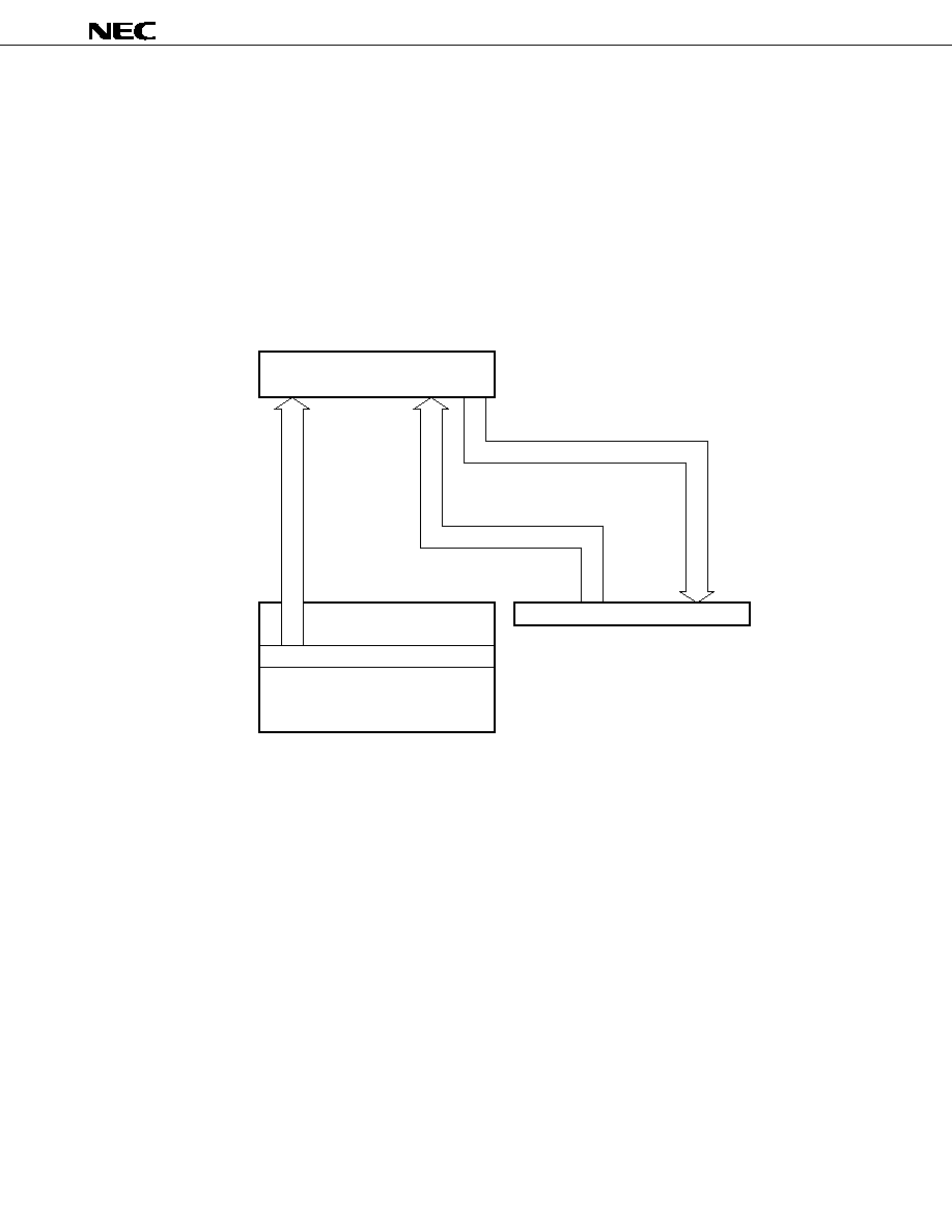
85
�
PD17704, 17705, 17707, 17708, 17709
9. DATA BUFFER (DBF)
9.1 Outline of Data Buffer
Figure 9-1 outlines the data buffer.
The data buffer is located on the data memory and has the following two functions.
�
Reads constant data on the program memory (table reference)
�
Transfers data with the peripheral hardware units
Figure 9-1. Outline of Data Buffr
Data buffer
Data write (PUT)
Data read (GET)
Table reference
(MOVT)
Peripheral hardware
Constant data
Program memory

�
PD17704, 17705, 17707, 17708, 17709
86
9.2 Data Buffer
9.2.1 Configuration of data buffer
Figure 9-2 shows the configuration of the data buffer.
As shown in the figure, the data buffer consists of a total of 16 bits of addresses 0CH through 0FH of BANK
0 on the data memory.
The 16-bit data is configured with bit 3 of address 0CH as the MSB and bit 0 of address 0FH as the LSB.
Because the data buffer is located on the data memory, it can be manipulated by all data memory manipulation
instructions.
Figure 9-2. Configuration of Data Buffer
Column address
0
1
2
3
4
5
6
7
0
1
2
3
4
5
6
7
8
9
A
B
C
D
E
F
BANK0
BANK1
BANK2
BANK14
BANK15
System register
Address
Bit
Bit
Signal
Data
b
3
b
15
b
2
b
14
b
1
b
13
b
0
b
12
DBF3
0CH
b
3
b
11
b
2
b
10
b
1
b
9
b
0
b
8
DBF2
0DH
b
3
b
7
b
2
b
6
b
1
b
5
b
0
b
4
DBF1
0EH
b
3
b
3
b
2
b
2
b
1
b
1
b
0
b
0
DBF0
0FH
Data memory
Data buffer
Remark
Data buffer (DBF)
Row address
Data memory
M
S
B
L
S
B
�
Data
The PD17704 and 17705 do
not have BANKs 6 through 14.
The PD17707 and 17705 do
not have BANKs 6 through 14.
�

87
�
PD17704, 17705, 17707, 17708, 17709
9.2.2 Table reference instruction ("MOVT DBF, @AR")
This instruction moves the contents of the program memory addressed by the contents of the address register
to the data buffer.
The number of bits transferred by the table reference instruction can be specified by MOVT selection register
(address 07H) of the control registers.
When 8-bit data is transferred, it is read to DBF1 and 0.
When the table reference instruction is used, one stack level is used.
All the addresses of the program memory can be referenced by the table reference instruction.
9.2.3 Peripheral hardware control instructions ("PUT" and "GET")
The operations of the "PUT" and "GET" instructions are as follows:
(1) GET DBF, p
Reads the data of a peripheral register addressed by "p" to the data buffer.
(2) PUT p, DBF
Sets the data of the data buffer to a peripheral register addressed by "p".
9.3 Relationships between Peripheral Hardware and Data Buffer
Table 9-1 shows the relationships between the peripheral hardware and the data buffer.

�
PD17704, 17705, 17707, 17708, 17709
88
Table 9-1. Relationships between Peripheral Hardware and Data Buffer (1/2)
Peripheral Hardware
Peripheral Register Transferring Data with Data Buffer
Name
Symbol
Peripheral
Execution of
I/O
Actual
address
PUT/GET
bit
bit
instruction
A/D converter
A/D converter reference
ADCR
02H
PUT/GET
8
8
voltage setting register
Serial interface
Serial interface 0
Presettable shift register 0
SIO0SFR
03H
PUT/GET
8
8
Serial interface 1
Presettable shift register 1
SIO1SFR
04H
Timer 0
Timer 0 modulo register
TM0M
1AH
PUT/GET
8
8
Timer 0 counter
TM0C
1BH
GET
8
8
Timer 1
Timer 1 modulo register
TM1M
1CH
PUT/GET
8
8
Timer 1 counter
TM1C
1DH
GET
8
8
Timer 2
Timer 2 modulo register
TM2M
1EH
PUT/GET
8
8
Timer 2 counter
TM2C
1FH
GET
8
8
Address register
Address register
AR
40H
PUT/GET
16
16
Data buffer stack
DBF stack
DBFSTK
41H
PUT/GET
16
16
PLL frequency synthesizer
Note
PLL data register
PLLR
42H
PUT/GET
16
16
Frequency counter
IF counter data register
IFC
43H
GET
16
16
D/A converter
P1B0/PWM0 pin
PWM data register 0
PWMR0
44H
PUT/GET
16
9
(PWM output)
P1B1/PWM1 pin
PWM data register 1
PWMR1
45H
P1B2/PWM2 pin
PWM data register 2
PWMR2
46H
PUT/GET
16
9
Timer 3
Timer 3 modulo register
TM3M
8
Note
The programmable counter of the PLL frequency synthesizer is configured of 17 bits, of which the high-
order 16 bits indicate the PLL data register (PLLR) and the low-order bits are allocated to the PLLSCNF
flag (the third bit of address 10H).
For details, refer to 17. PLL FREQUENCY SYNTHESIZER.

89
�
PD17704, 17705, 17707, 17708, 17709
Table 9-1. Relationships between Peripheral Hardware and Data Buffer (2/2)
At Reset
Clock
Function
Power-ON WDT&SP
CE
Stop
reset
reset
reset
0
0
0
Note
0
Note
Sets compare voltage V
ADCREF
of A/D converter
Undefined Undefined Undefined Undefined
Sets serial-out data and reads serial-in data
FF
FF
Retained
FF
Sets modulo register value of timer 0
0
0
Retained
0
Reads count value of timer 0 counter
FF
FF
Retained
FF
Sets modulo register value of timer 1
0
0
Retained
0
Reads count value of timer 1 counter
FF
FF
Retained
FF
Sets modulo register value of timer 2
0
0
Retained
0
Reads count value of timer 2 counter
0
0
0
Retained
Transfers data with address register
Undefined Undefined Retained
Retained
Saves data of data buffer
Undefined Undefined Retained
Retained
Sets division value (N value) of PLL
0
0
0
0
Reads count value of frequency counter
1FF
1FF
Retained
1FF
Sets duty of output signal of D/A converter
Sets duty of output signal of D/A converter (multiplexed with modulo register of timer 3)
Sets modulo register value of timer 3
Note
Value in hardare mode. "Retained" in software mode.

�
PD17704, 17705, 17707, 17708, 17709
90
9.4 Cautions on Using Data Buffer
Keep the following points in mind concerning the unused peripheral addresses, write-only peripheral register
(PUT only), and read-only peripheral register (GET only) when transferring data with the peripheral hardware
via data buffer.
�
An "undefined value" is read if a write-only register is read.
�
Nothing is affected even if a read-only register is written.
�
An "undefined value" is read if an unused address is read. Nor is anything affected if this address is written.

91
�
PD17704, 17705, 17707, 17708, 17709
10. DATA BUFFER STACK
10.1 Outline of Data Buffer Stack
Figure 10-1 outlines the data buffer stack.
As shown in the figure, the data buffer stack consists of a data buffer stack pointer and data buffer stack
registers.
The data buffer stack saves or restores the contents of the data buffer when the "PUT" or "GET" instruction
is executed.
Therefore, the contents of the data buffer can be saved by one instruction when an interrupt is accepted.
Figure 10-1. Outline of Data Buffer Stack
10.2 Data Buffer Stack Register
Figure 10-2 shows the configuration of the data buffer stack registers.
As shown in the figure, the data buffer stack registers consist of four 16-bit registers.
The contents of the data buffer are saved by executing the "PUT" instruction, and the saved data is restored
by executing the "GET" instruction.
The data buffer contents can be successively saved up to 4 levels.
Data buffer
stack pointer
DBF
Data buffer stack registers
Address specification

�
PD17704, 17705, 17707, 17708, 17709
92
Figure 10-2. Configuration of Data Buffer Stack Register
DBF3
DBF2
DBF1
DBF0
16 bits
Data buffer
Transfer data
Valid data
b
15
b
14
b
13
b
12
b
11
b
10
b
9
b
8
b
7
b
6
b
5
b
4
b
3
b
2
b
1
b
0
Data buffer stack register
DBFSTK
41H
GET
PUT
Saves contents of data
buffer up to 4 levels
Bit
Name
Symbol
Address
Data

93
�
PD17704, 17705, 17707, 17708, 17709
10.3 Data Buffer Stack Pointer
The data buffer stack pointer detects the multiplexing level of the data buffer stack registers.
When the "PUT" instruction is executed to the data buffer stack, the value of the data buffer stack pointer
is incremented by one; when the "GET" instruction is executed, the value of the pointer is decremented by one.
The data buffer stack pointer can be only read and cannot be written.
The configuration and function of the data buffer stack pointer are illustrated below.
Name
Flag symbol
b
3
0
b
2
0
b
1
D
B
F
S
P
1
b
0
D
B
F
S
P
0
Address
04H
Read/Write
R
Data buffer stack pointer
Power-ON reset
WDT&SP reset
CE reset
Clock stop
0
1
0
1
Level 0
Level 1
Level 2
Level 3
Detects multiplexing level of data buffer stack
0
0
1
1
Retained
Fixed to "0"
0
0
0
0
0
0
0
0
At reset

�
PD17704, 17705, 17707, 17708, 17709
94
10.4 Operation of Data Buffer Stack
Figure 10-3 shows the operation of the data buffer stack.
As shown in the figure, when the PUT instruction is executed, the contents of the data buffer are transferred
to a data buffer stack register specified by the stack pointer, and the stack pointer is incremented by one.
When the GET instruction is executed, the contents of a data buffer stack register specified by the stack
pointer are transferred to the data buffer, and the stack pointer is decremented by one.
Therefore, note that the value of the stack pointer is set to 1 if data has been written once because its initial
value is 0, and that the stack pointer is set to 0 when data has been written four times.
Note that when writing (PUT) exceeding four levels, the first data are discarded.
Figure 10-3. Operation of Data Buffer Stack
(a) If writing does not exceed level 4
(b) If writing exceeds level 4
Undefined
Undefined
Undefined
Undefined
V
DD
A
Undefined
Undefined
Undefined
PUT
A
B
Undefined
Undefined
PUT
A
B
Undefined
Undefined
GET
A
B
Undefined
Undefined
GET
0
1
2
3
A
Undefined
Undefined
Undefined
PUT
A
B
Undefined
Undefined
PUT
A
B
C
Undefined
PUT
A
B
C
D
E
B
C
D
E
B
C
D
GET
E
B
C
D
GET
PUT
PUT
0
1
2
3

95
�
PD17704, 17705, 17707, 17708, 17709
10.5 Using Data Buffer Stack
A program example is shown below.
Example To save the contents of the data buffer and address register by using INT0 interrupt routine (the
contents of the data buffer and address register are not automatically saved when an interrupt
occurs).
START:
BR
INITIAL
; Reset address
; Interrupt vector address
NOP
; SI01
NOP
; SI00
NOP
; TM3
NOP
; TM2
NOP
; TM1
NOP
; TM0
NOP
; INT4
NOP
; INT3
NOP
; INT2
NOP
; INT1
BR
INTINT0
; INT0
NOP
; Down edge of CE
INTINT0:
PUT
DBFSTK, DBF ; Saves contents of DBF to first level of data buffer
; stack (DBFSTK)
GET
DBF, AR
; Transfers contents of address register (AR) to DBF
PUT
DBFSTK, DBF ; Saves contents of AR to second level of data buffer
; stack
Processing B
; INT0 interrupt processing
GET
DBF, DBFSTK ; Restores second level of data buffer stack to data buffer,
PUT
AR, DBF
; and restores contents of data buffer to address register
GET
DBF, DBFSTK ; Restores first level of data buffer stack to data buffer
EI
RETI
INITIAL:
SET1 IP0
EI
LOOP:
Processing A
BR
LOOP
END
10.6 Cautions on Using Data Buffer Stack
The contents of the data buffer stack are not automatically saved when an interrupt is accepted, and therefore,
must be saved by software.
Even when a bank of the data memory other than BANK0 is specified, the contents of the data buffer (existing
in BANK0) can be saved or restored by using the "PUT" and "GET" instructions.
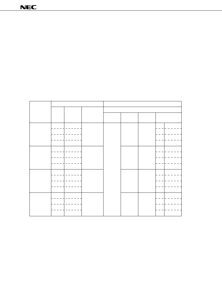
�
PD17704, 17705, 17707, 17708, 17709
96
11. GENERAL-PURPOSE PORT
The general-purpose ports output high-level, low-level, or floating signals to external circuits, and read high-
level or low-level signals from external circuits.
11.1 Outline of General-purpose Port
Table 11-1 shows the relationships between each port and port register.
The general-prupose ports are classified into I/O, input, and output ports.
The I/O ports are further subclassified into bit I/O ports that can be set in the input or output mode in 1-bit
(1-pin) units, and group I/O ports that can be set in the input or output mode in 4-bit (4-pin) units. The inut or
output mode of each I/O port is specified by the port input/output selection registers (addresses 60H through
6FH) of BANK15.
Table 11-1. Relationships between Port (Pin) and Port Register (1/3)
Port
Pin
Data Setting Method
No.
Symbol
I/O
Port register (data memory)
Bank
Address
Symbol
Bit symbol
(reserved word)
Port 0A
63
P0A3
I/O (bit I/O)
BANK0
70H
P0A
b
3
P0A3
64
P0A2
b
2
P0A2
65
P0A1
b
1
P0A1
66
P0A0
b
0
P0A0
Port 0B
67
P0B3
I/O (bit I/O)
71H
P0B
b
3
P0B3
68
P0B2
b
2
P0B2
69
P0B1
b
1
P0B1
70
P0B0
b
0
P0B0
Port 0C
59
P0C3
I/O (bit I/O)
72H
P0C
b
3
P0C3
60
P0C2
b
2
P0C2
61
P0C1
b
1
P0C1
62
P0C0
b
0
P0C0
Port 0D
22
P0D3
Input
73H
P0D
b
3
P0D3
23
P0D2
b
2
P0D2
24
P0D1
b
1
P0D1
25
P0D0
b
0
P0D0
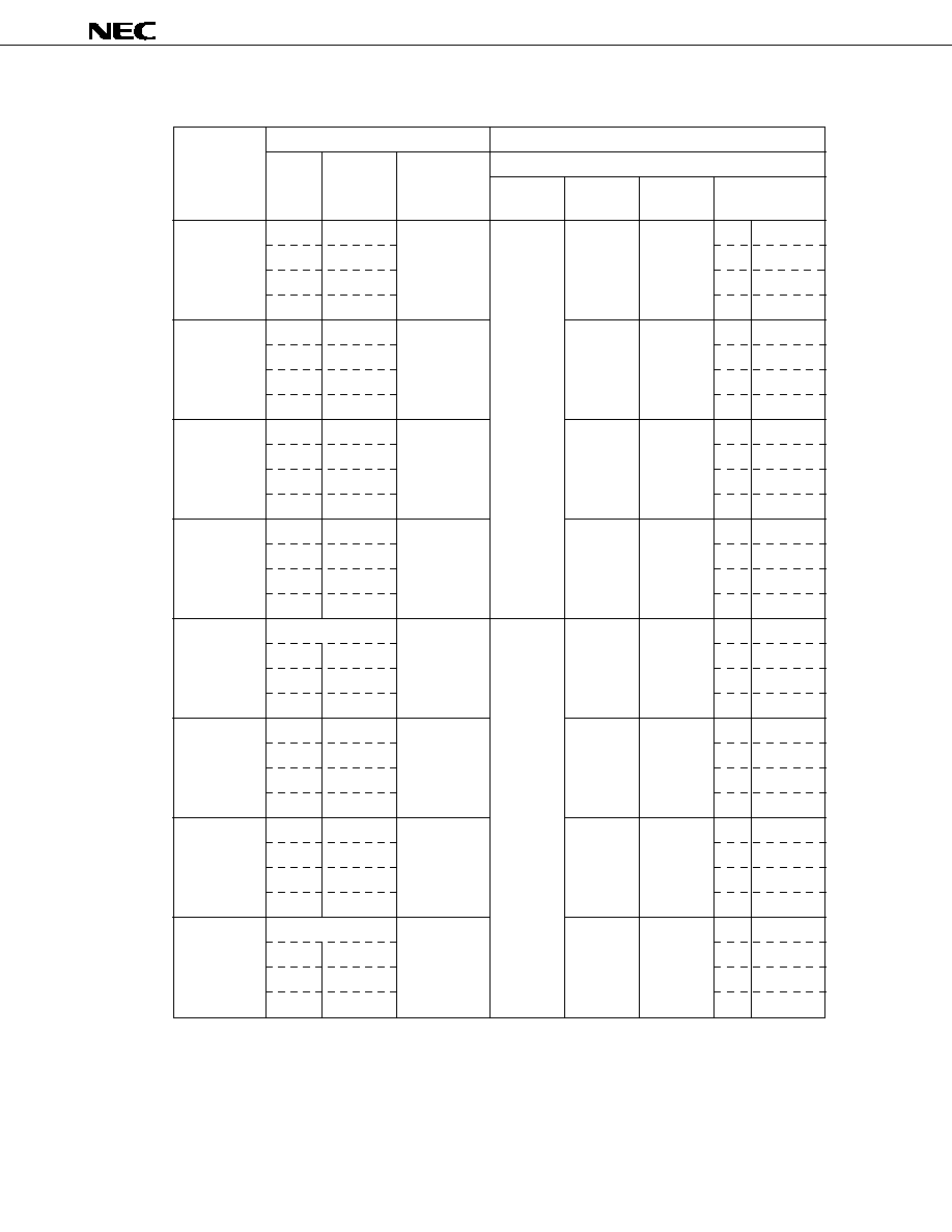
97
�
PD17704, 17705, 17707, 17708, 17709
Table 11-1. Relationships between Port (Pin) and Port Register (2/3)
Port
Pin
Data Setting Method
No.
Symbol
I/O
Port register (data memory)
Bank
Address
Symbol
Bit symbol
(reserved word)
Port 1A
2
P1A3
Input
BANK1
70H
P1A
b
3
P1A3
3
P1A2
b
2
P1A2
4
P1A1
b
1
P1A1
5
P1A0
b
0
P1A0
Port 1B
17
P1B3
Output
71H
P1B
b
3
P1B3
18
P1B2
b
2
P1B2
19
P1B1
b
1
P1B1
20
P1B0
b
0
P1B0
Port 1C
26
P1C3
Input
72H
P1C
b
3
P1C3
27
P1C2
b
2
P1C2
28
P1C1
b
1
P1C1
29
P1C0
b
0
P1C0
Port 1D
37
P1D3
I/O (bit I/O)
73H
P1D
b
3
P1D3
38
P1D2
b
2
P1D2
39
P1D1
b
1
P1D1
40
P1D0
b
0
P1D0
Port 2A
No pin
I/O (bit I/O)
BANK2
70H
P2A
b
3
�
14
P2A2
b
2
P2A2
15
P2A1
b
1
P2A1
16
P2A0
b
0
P2A0
Port 2B
43
P2B3
I/O (bit I/O)
71H
P2B
b
3
P2B3
44
P2B2
b
2
P2B2
45
P2B1
b
1
P2B1
46
P2B0
b
0
P2B0
Port 2C
55
P2C3
I/O
72H
P2C
b
3
P2C3
56
P2C2
(bit I/O)
b
2
P2C2
57
P2C1
b
1
P2C1
58
P2C0
b
0
P2C0
Port 2D
No pin
I/O (bit I/O)
73H
P2D
b
3
�
71
P2D2
b
2
P2D2
72
P2D1
b
1
P2D1
73
P2D0
b
0
P2D0

�
PD17704, 17705, 17707, 17708, 17709
98
Table 11-1. Relationships between Port (Pin) and Port Register (3/3)
Port
Pin
Data Setting Method
No.
Symbol
I/O
Port register (data memory)
Bank
Address
Symbol
Bit symbol
(reserved word)
Port 3A
6
P3A3
I/O
BANK3
70H
P3A
b
3
P3A3
7
P3A2
(group I/O)
b
2
P3A2
8
P3A1
b
1
P3A1
9
P3A0
b
0
P3A0
Port 3B
10
P3B3
I/O
71H
P3B
b
3
P3B3
11
P3B2
(group I/O)
b
2
P3B2
12
P3B1
b
1
P3B1
13
P3B0
b
0
P3B0
Port 3C
47
P3C3
I/O
72H
P3C
b
3
P3C3
48
P3C2
(group I/O)
b
2
P3C2
49
P3C1
b
1
P3C1
50
P3C0
b
0
P3C0
Port 3D
51
P3D3
I/O
73H
P3D
b
3
P3D3
52
P3D2
(group I/O)
b
2
P3D2
53
P3D1
b
1
P3D1
54
P3D0
b
0
P3D0
�
No pin
�
BANK4
70H-73H
�
Fixed to "0"
|
BANK15
Note
Note
The
�
PD17704 and 17705 do not have BANKs 6 through 14.
�
PD17707 and 17708 do not have BANKs 10 through 14.

99
�
PD17704, 17705, 17707, 17708, 17709
11.2 General-Purpose I/O Port (P0A, P0B, P0C, P1D, P2A, P2B, P2C, P2D, P3A, P3B, P3C, P3D)
11.2.1 Configuration of I/O port
The following paragraphs (1) and (2) show the configuration of the I/O ports.
(1) P0A (P0A1, P0A0)
P0B (P0B3, P0B2, P0B1, P0B0)
P0C (P0C3, P0C2, P0C1, P0C0)
P1D (P1D3, P1D2, P1D1, P1D0)
P2A (P2A2, P2A1, P2A0)
P2B (P2B3, P2B2, P2B1, P2B0)
P2C (P2C3, P2C2, P2C1, P2C0)
P2D (P2D2, P2D1, P2D0)
P3A (P3A3, P3A2, P3A1, P3A0)
P3B (P3B3, P3B2, P3B1, P3B0)
P3C (P3C3, P3C2, P3C1, P3C0)
P3D (P3D3, P3D2, P3D1, P3D0)
Note
This is an internal signal that is output when the clock stop instruction is executed, and this circuit
is designed not to increase the current consumption due to noise even if it is floated.
V
DD
V
DD
I/O selection flag
Output latch
1
0
Read instruction
Port register
(1 bit)
Write instruction
CKSTOP
Note

�
PD17704, 17705, 17707, 17708, 17709
100
(2) P0A (P0A3, P0A2)
Note
This is an internal signal that is output when the clock stop instruction is executed, and this circuit
is designed not to increase the current consumption due to noise even if it is floated.
11.2.2 Using I/O port
The input or output mode of the I/O ports is set by I/O selection register P0A, P0B, P0C, P1D, P2A, P2B,
P2C, P2D, P3A, P3B, P3C, or P3D of the control registers.
Because P0A, P0B, P0C, P1D, P2A, P2B, P2C, and P2D are bit I/O ports, they can be set in the input or output
mode in 1-bit units.
P3A, P3B, P3C, and P3D are group I/O ports, and therefore they are set in the input or output mode in 4-
bit units.
Setting the output data of or reading the input data of a port is carried out by executing an instruction that
writes data to or reads data from the port.
11.2.3 shows the configuration of the I/O selection register of each port.
11.2.4 and 11.2.5 describe how each port is used as an input or output port.
11.2.6 describes the points to be noted when using the I/O ports.
V
DD
I/O selection flag
Output latch
Read instruction
Port register
(1 bit)
Write instruction
CKSTOP
Note

101
�
PD17704, 17705, 17707, 17708, 17709
11.2.3 I/O port I/O selection register
The following I/O selection registers of the I/O ports are available.
�
Port 0A bit I/O selection register
�
Port 0B bit I/O selection register
�
Port 0C bit I/O selection register
�
Port 1D bit I/O selection register
�
Port 2A bit I/O selection register
�
Port 2B bit I/O selection register
�
Port 2C bit I/O selection register
�
Port 2D bit I/O selection register
�
Group I/O selection registers (port 3A, port 3B, port 3C, port 3D)
Each I/O selection register sets the input or output mode of the corresponding port pin.
The following paragraphs (1) through (9) descibe the configuration and functions of the above I/O selection
registers.

�
PD17704, 17705, 17707, 17708, 17709
102
(1) Port 0A bit I/O selection register
Name
Flag symbol
b
3
P
0
A
B
I
O
3
b
2
P
0
A
B
I
O
2
b
1
P
0
A
B
I
O
1
b
0
P
0
A
B
I
O
0
Address
(BANK15)
6FH
Read/Write
R/W
Port 0A bit I/O selection
Power-ON reset
WDT&SP reset
CE reset
Clock stop
0
1
Sets P0A0 pin in input mode
Sets P0A0 pin in output mode
Sets input/output mode of port
Retained
Retained
Sets P0A1 pin in input mode
Sets P0A1 pin in output mode
Sets input/output mode of port
0
1
Sets P0A2 pin in input mode
Sets P0A2 pin in output mode
Sets input/output mode of port
0
1
Sets P0A3 pin in input mode
Sets P0A3 pin in output mode
Sets input/output mode of port
0
1
0
0
0
0
0
0
0
0
At reset
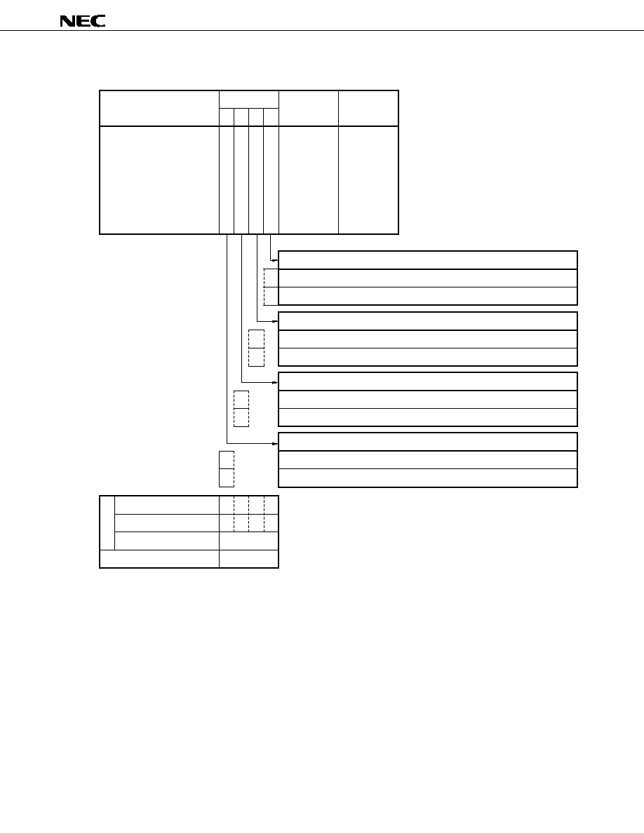
103
�
PD17704, 17705, 17707, 17708, 17709
(2) Port 0B bit I/O selection register
Name
Flag symbol
b
3
P
0
B
B
I
O
3
b
2
P
0
B
B
I
O
2
b
1
P
0
B
B
I
O
1
b
0
P
0
B
B
I
O
0
Address
(BANK15)
6EH
Read/Write
R/W
Port 0B bit I/O selection
Power-ON reset
WDT&SP reset
CE reset
Clock stop
0
1
Sets P0B0 pin in input mode
Sets P0B0 pin in output mode
Sets input/output mode of port
Retained
Retained
Sets P0B1 pin in input mode
Sets P0B1 pin in output mode
Sets input/output mode of port
0
1
Sets P0B2 pin in input mode
Sets P0B2 pin in output mode
Sets input/output mode of port
0
1
Sets P0B3 pin in input mode
Sets P0B3 pin in output mode
Sets input/output mode of port
0
1
0
0
0
0
0
0
0
0
At reset
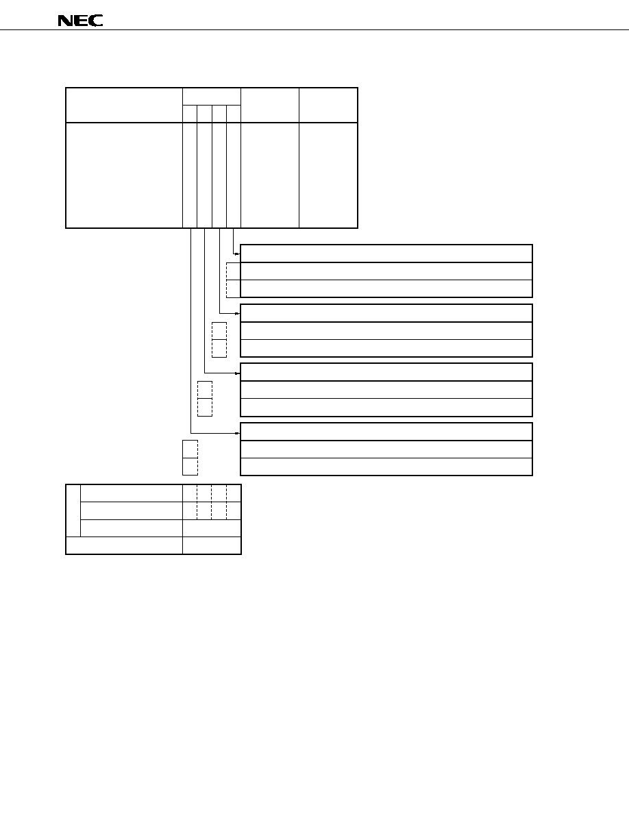
�
PD17704, 17705, 17707, 17708, 17709
104
(3) Port 0C bit I/O selection register
Name
Flag symbol
b
3
P
0
C
B
I
O
3
b
2
P
0
C
B
I
O
2
b
1
P
0
C
B
I
O
1
b
0
P
0
C
B
I
O
0
Address
(BANK15)
6DH
Read/Write
R/W
Port 0C bit I/O selection
Power-ON reset
WDT&SP reset
CE reset
Clock stop
0
1
Sets P0C0 pin in input mode
Sets P0C0 pin in output mode
Sets input/output mode of port
Retained
Retained
Sets P0C1 pin in input mode
Sets P0C1 pin in output mode
Sets input/output mode of port
0
1
Sets P0C2 pin in input mode
Sets P0C2 pin in output mode
Sets input/output mode of port
0
1
Sets P0C3 pin in input mode
Sets P0C3 pin in output mode
Sets input/output mode of port
0
1
0
0
0
0
0
0
0
0
At reset
105
�
PD17704, 17705, 17707, 17708, 17709
(4) Port 1D bit I/O selection register
Name
Flag symbol
b
3
P
1
D
B
I
O
3
b
2
P
1
D
B
I
O
2
b
1
P
1
D
B
I
O
1
b
0
P
1
D
B
I
O
0
Address
(BANK15)
6CH
Read/Write
R/W
Port 1D bit I/O selection
Power-ON reset
WDT&SP reset
CE reset
Clock stop
0
1
Sets P1D0 pin in input mode
Sets P1D0 pin in output mode
Sets input/output mode of port
Retained
Retained
Sets P1D1 pin in input mode
Sets P1D1 pin in output mode
Sets input/output mode of port
0
1
Sets P1D2 pin in input mode
Sets P1D2 pin in output mode
Sets input/output mode of port
0
1
Sets P1D3 pin in input mode
Sets P1D3 pin in output mode
Sets input/output mode of port
0
1
0
0
0
0
0
0
0
0
At reset

�
PD17704, 17705, 17707, 17708, 17709
106
(5) Port 2A bit I/O selection register
Name
Flag symbol
b
3
0
b
2
P
2
A
B
I
O
2
b
1
P
2
A
B
I
O
1
b
0
P
2
A
B
I
O
0
Address
(BANK15)
6BH
Read/Write
R/W
Port 2A bit I/O selection
Power-ON reset
WDT&SP reset
CE reset
Clock stop
0
1
Sets P2A0 pin in input mode
Sets P2A0 pin in output mode
Sets input/output mode of port
Retained
Retained
Sets P2A1 pin in input mode
Sets P2A1 pin in output mode
Sets input/output mode of port
0
1
Sets P2A2 pin in input mode
Sets P2A2 pin in output mode
Sets input/output mode of port
0
1
Fixed to "0"
0
0
0
0
0
0
0
At reset

107
�
PD17704, 17705, 17707, 17708, 17709
(6) Port 2B bit I/O selection register
Name
Flag symbol
b
3
P
2
B
B
I
O
3
b
2
P
2
B
B
I
O
2
b
1
P
2
B
B
I
O
1
b
0
P
2
B
B
I
O
0
Address
(BANK15)
6AH
Read/Write
R/W
Port 2B bit I/O selection
Power-ON reset
WDT&SP reset
CE reset
Clock stop
0
1
Sets P2B0 pin in input mode
Sets P2B0 pin in output mode
Sets input/output mode of port
Retained
Retained
Sets P2B1 pin in input mode
Sets P2B1 pin in output mode
Sets input/output mode of port
0
1
Sets P2B2 pin in input mode
Sets P2B2 pin in output mode
Sets input/output mode of port
0
1
Sets P2B3 pin in input mode
Sets P2B3 pin in output mode
Sets input/output mode of port
0
1
0
0
0
0
0
0
0
0
At reset
�
PD17704, 17705, 17707, 17708, 17709
108
(7) Port 2C bit I/O selection register
Name
Flag symbol
b
3
P
2
C
B
I
O
3
b
2
P
2
C
B
I
O
2
b
1
P
2
C
B
I
O
1
b
0
P
2
C
B
I
O
0
Address
(BANK15)
69H
Read/Write
R/W
Port 2C bit I/O selection
Power-ON reset
WDT&SP reset
CE reset
Clock stop
0
1
Sets P2C0 pin in input mode
Sets P2C0 pin in output mode
Sets input/output mode of port
Retained
Retained
Sets P2C1 pin in input mode
Sets P2C1 pin in output mode
Sets input/output mode of port
0
1
Sets P2C2 pin in input mode
Sets P2C2 pin in output mode
Sets input/output mode of port
0
1
Sets P2C3 pin in input mode
Sets P2C3 pin in output mode
Sets input/output mode of port
0
1
0
0
0
0
0
0
0
0
At reset
109
�
PD17704, 17705, 17707, 17708, 17709
(8) Port 2D bit I/O selection register
Name
Flag symbol
b
3
0
b
2
P
2
D
B
I
O
2
b
1
P
2
D
B
I
O
1
b
0
P
2
D
B
I
O
0
Address
(BANK15)
68H
Read/Write
R/W
Port 2D bit I/O selection
Power-ON reset
WDT&SP reset
CE reset
Clock stop
0
1
Sets P2D0 pin in input mode
Sets P2D0 pin in output mode
Sets input/output mode of port
Retained
Retained
Sets P2D1 pin in input mode
Sets P2D1 pin in output mode
Sets input/output mode of port
0
1
Sets P2D2 pin in input mode
Sets P2D2 pin in output mode
Sets input/output mode of port
0
1
Fixed to "0"
0
0
0
0
0
0
0
At reset

�
PD17704, 17705, 17707, 17708, 17709
110
(9) Group I/O selection register (ports 3A, 3B, 3C, 3D)
Name
Flag symbol
b
3
P
3
D
G
I
O
b
2
P
3
C
G
I
O
b
1
P
3
B
G
I
O
b
0
P
3
A
G
I
O
Address
(BANK15)
67H
Read/Write
R/W
Group I/O selection
Power-ON reset
WDT&SP reset
CE reset
Clock stop
0
1
Sets P3A0 through P3A3 pins in input mode
Sets P3A0 through P3A3 pins in output mode
Sets input/output mode of port
Retained
Retained
Sets P3B0 through P3B3 pins in input mode
Sets P3B0 through P3B3 pins in output mode
Sets input/output mode of port
0
1
Sets P3C0 through P3C3 pins in input mode
Sets P3C0 through P3C3 pins in output mode
Sets input/output mode of port
0
1
Sets P3D0 through P3D3 pins in input mode
Sets P3D0 through P3D3 pins in output mode
Sets input/output mode of port
0
1
0
0
0
0
0
0
0
0
At reset

111
�
PD17704, 17705, 17707, 17708, 17709
11.2.4 When using I/O port as input port
The port pin to be set in the input mode is selected by the I/O selection register corresponding to the port.
Ports P0A, P0B, P0C, P1D, P2A, P2B, P2C, and P2D can be set in the input or output mode in 1-bit units.
P3A, P3B, P3C, and P3D can be set in the input or output mode in 4-bit units.
The pin set in the input mode is floated (Hi-Z) and waits for input of an external signal.
The input data is read by executing a read instruction (such as SKT) to the port register corresponding to
the port pin.
"1" is read from the port register when a high level is input to the corresponding port pin; when a low level
is input to the port pin, "0" is read from the register.
When a write instruction (such as MOV) is executed to the port register corresponding to the pin set in the
input mode, the contents of the output latch are rewritten.
11.2.5 When using I/O port as output port
The port pin to be set in the output mode is selected by the I/O selection register corresponding to the port.
Ports P0A, P0B, P0C, P1D, P2A, P2B, P2C, and P2D can be set in the input or output mode in 1-bit units.
P3A, P3B, P3C, and P3D can be set in the input or output mode in 4-bit units.
The pin set in the output mode outputs the contents of the output latch.
The output data is set by executing a write instruction (such as MOV) to the port register corresponding to
the port pin.
Write "1" to the port register to output a high level to the port pin; write "0" to output a low level. The port pin
can be also floated (Hi-Z) if it is set in the input mode.
If a read instruction (such as SKT) is executed to the port register corresponding to a port pin set in the output
mode, the contents of the output latch are read.
Note, however, that the contents of the output latch of the P0A3 and P0A2 pins may differ from the read
contents because the status of these pins are read as are (refer to 11.2.6).
11.2.6 Cautions on using I/O port (P0A3 and P0A2 pins)
When using the P0A3 and P0A2 pins in the output mode, the contents of the output latch may be rewritten
as shown in the example below.
Example To set the P0A3 and P0A2 pins in the output mode
BANK15
INITFLG P0ABI03, P0ABI02, NOT P0ABI01, NOT P0ABI00 ; Sets P0A3 and P0A2 pins in
output mode
INITFLG P0A3, P0A2, NOT P0A1, NOT P0A0
; Outputs high level to P0A3 and
P0A2 pins
; <1>
CLR1
P0A3
; Outputs low level to P0A3 pin
MACRO EXTEND
AND
.MF.P0A3 SHR 4, #.DF.(NOT P0A3 AND 0FH)
If the P0A2 pin is externally made low when the instruction in the above example <1> is executed,
the contents of the output latch of the P0A2 pin are rewritten to "0" by the CLR1 instruction.
In other words, if an instruction that reads the contents of port register P0A is executed while the
P0A3 or P0A2 pin is set in the output mode, the contents of the output latch are rewritten to the
pin level at that time, regardless of the previous status.

�
PD17704, 17705, 17707, 17708, 17709
112
11.2.7 Status of I/O port at reset
(1) At power-ON reset
All the I/O ports are set in the input mode.
The contents of the output latch are reset to "0".
(2) At WDT&SP reset
All the I/O ports are set in the input mode.
The contents of the output latch are reset to "0".
(3) At CE reset
The setting of the input or output mode is retained.
The contents of the output latch are also retained.
(4) On execution of clock stop instruction
The setting of the input or output mode is retained.
The contents of the output latch are also retained.
(5) In halt status
The previous status is retained.

113
�
PD17704, 17705, 17707, 17708, 17709
11.3 General-Purpose Input Port (P0D, P1A, P1C)
11.3.1 Configuration of input port
The following paragraphs (1) and (2) show the configuration of the input port.
(1) P0D (P0D3, P0D2, P0D1, P0D0)
Note
This is an internal signal output on execution of the clock stop instruction, and its circuit is
designed not to increase the current consumption due to noise even if the pin is floated.
(2) P1A (P1A3, P1A2, P1A1, P1A0)
P1C (P1C3, P1C2, P1C1, P1C0)
Note
This is an internal signal output on execution of the clock stop instruction, and its circuit is
designed not to increase the current consumption due to noise even if the pin is floated. (Except
P1A3, P1A2, P1A0)
V
DD
Write instruction
Read instruction
Port register
(1 bit)
CKSTOP
Note
P0DPLD flag
High-ON resistance
Input latch
To A/D converter
V
DD
To frequency counter or A/D converter
Write instruction
Read instruction
Port register
(1 bit)
CKSTOP
Note

�
PD17704, 17705, 17707, 17708, 17709
114
11.3.2 Using input port
The input data is read by executing a read instruction (such as SKT) to the port register corresponding to
the port pin.
"1" is read from the port register when a high level is input to the corresponding port pin; when a low level
is input to the port pin, "0" is read from the register.
Nothing is affected even if a write instruction (such as MOV) is executed to the port register.
P0D has a pull-down resistor that can be connected or disconnected by software in 1-bit units. The pull-down
resistor is connected when "0" is written to the corresponding bit of the port 0D pull-down resistor selection
register. When "1" is written to the corresponding bit of this register, the pull-down resistor is disconnected.
11.3.3 Port 0D pull-down resistor selection register
The port 0D pull-down resistor selection register specifies whether a pull-down resistor is connected to P0D3
through P0D0 pins. The configuration and function of this register are illustrated below.
�
Port 0D pull-down resistor selection register
Name
Flag symbol
b
3
P
0
D
P
L
D
3
b
2
P
0
D
P
L
D
2
b
1
P
0
D
P
L
D
1
b
0
P
0
D
P
L
D
0
Address
(BANK15)
66H
Read/Write
R/W
Port 0D pull-down resistor
selection
Power-ON reset
WDT&SP reset
CE reset
Clock stop
0
1
Connects pull-down resistor to P0D0 pin
Disconnects pull-down resistor from P0D0 pin
Selects pull-down resistor of P0D0 pin
Retained
Retained
Connects pull-down resistor to P0D1 pin
Disconnects pull-down resistor from P0D1 pin
Selects pull-down resistor of P0D1 pin
0
1
Connects pull-down resistor to P0D2 pin
Disconnects pull-down resistor from P0D2 pin
Selects pull-down resistor of P0D2 pin
0
1
Connects pull-down resistor to P0D3 pin
Disconnects pull-down resistor from P0D3 pin
Selects pull-down resistor of P0D3 pin
0
1
0
0
0
0
0
0
0
0
At reset

115
�
PD17704, 17705, 17707, 17708, 17709
11.3.4 Status of input port at reset
(1) At power-ON reset
All the input ports are set in the input mode.
All the pull-down resistors of P0D are connected.
(2) At WDT&SP reset
All the input ports are set in the input mode.
All the pull-down resistors of P0D are connected.
(3) At CE reset
The input ports are set in the input mode.
The pull-down resistors of P0D retain the previous status.
(4) On execution of clock stop instruction
The input ports are set in the input mode.
The pull-down resistors of P0D retain the previous status.
(5) In halt status
The previous status is retained.

�
PD17704, 17705, 17707, 17708, 17709
116
11.4 General-Purpose Output Port (P1B)
11.4.1 Configuration of output port
The configuration of the output port is shown below.
(1) P1B (P1B3, P1B2, P1B1, P1B0)
11.4.2 Using output port
The output port outputs the contents of the output latch to each pin.
The output data is set by executing a write instruction (such as MOV) to the port register corresponding to
the port pin.
Write "1" to the port register to output a high level to the port pin; write "0" to output a low level.
However, because P1B is an N-ch open-drain output port, it is floated when it outputs a high level. Therefore,
an external pull-up resistor must be connected to this port.
If a read instruction (such as SKT) is executed to the port register, the contents of the output latch are read.
11.4.3 Status of output port at reset
(1) At power-ON reset
The contents of the output latch are output.
The contents of the output latch are reset to "0".
(2) At WDT&SP reset
The contents of the output latch are output.
The contents of the output latch are reset to "0".
(3) At CE reset
The contents of the output latch are output.
The contents of the output latch are retained.
(4) On execution of clock stop instruction
The contents of the output latch are output.
The contents of the output latch are retained.
(5) In halt status
The contents of the output latch are output.
The contents of the output latch are retained.
Output
latch
Read instruction
Port register
(1 bit)
Write instruction

117
�
PD17704, 17705, 17707, 17708, 17709
12. INTERRUPT
12.1 Outline of Interrupt Block
Figure 12-1 outlines the interrupt block.
As shown in the figure, the interrupt block temporarily stops the currently executed program and branches
execution to a vector address in response to an interrupt request output by a peripheral hardware unit.
The interrupt block consists of an "interrupt request servicing block" corresponding to each peripheral
hardware unit, "interrupt enable flip-flop" that enables all interrupts, "stack pointer" that is controlled when an
interrupt is accepted, "address stack registers", "program counter", and "interrupt stack".
The "interrupt control block" of each peripheral hardware unit consists of an "interrupt request flag (IRQ
���
)"
that detects the corresponding interrupt request, "interrupt enable flag (IP
���
)" that enables the interrupt, and
"vector address generator (VAG)" that specifies a vector address when the interrupt is accepted.
The
�
PD17709 has the following 12 types of maskable interrupts.
�
CE pin falling edge interrupt
�
INT0 through INT4 interrupts
�
Timer 0 through timer 3 interrupts
�
Serial interface 0 and serial interface 1 interrupts
When an interrupt is accepted, execution branches to a predetermined address, and the interrupt is serviced.
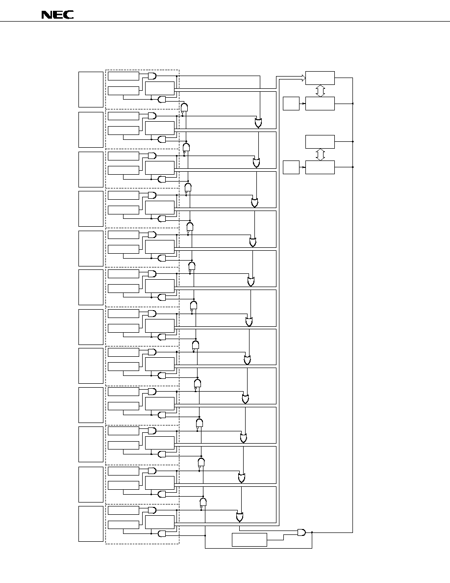
�
PD17704, 17705, 17707, 17708, 17709
118
Figure 12-1. Outline of Interrupt Block
Serial
interface 1
IPSIO1 flag
Serial
interface 0
IPSIO0 flag
Timer 3
IPTM3 flag
Timer 2
IPTM2 flag
Timer 1
IPTM1 flag
Timer 0
IPTM0 flag
INT4 pin
IP4 flag
INT3 pin
IP3 flag
INT2 pin
IP2 flag
INT1 pin
IP1 flag
INT0 pin
IP0 flag
CE pin
falling
IPCE flag
Program
counter
Address stack
registers
Stack
pointer
Interrupt stack
Pointer
Interrupt control block
Interrupt enable
flip-flop
DI, EI
instruction
IRQSIO1 flag
IRQSIO0 flag
IRQTM3 flag
IRQTM2 flag
IRQTM1 flag
IRQTM0 flag
IRQINT4 flag
IRQINT3 flag
IRQINT2 flag
IRQINT1 flag
IRQINT0 flag
IRQCE flag
Vector address
generator 01H
Vector address
generator 02H
Vector address
generator 03H
Vector address
generator 04H
Vector address
generator 05H
Vector address
generator 06H
Vector address
generator 07H
Vector address
generator 08H
Vector address
generator 09H
Vector address
generator 0AH
Vector address
generator 0BH
Vector address
generator 0CH
System
registers

119
�
PD17704, 17705, 17707, 17708, 17709
12.2 Interrupt Control Block
An interrupt control block is provided for each peripheral hardware unit. This block detects issuance of an
interrupt request, enables the interrupt, and generates a vector address when the interrupt is accepted.
12.2.1 Configuration and function of interrupt request flag (IRQ
���
)
Each interrupt request flag is set to 1 when an interrupt request is issued by the corresponding peripheral
hardware unit, and is reset to 0 when the interrupt is accepted.
Writing the interrupt request flag to "1" via a window register is equivalent to issuance of the interrupt request.
By detecting the interrupt request flag when an interrupt is not enabled, issuance status of each interrupt
request can be detected.
Once the interrupt request flag has been set, it is not reset until the corresponding interrupt is accepted, or
until "0" is written to the flag via a window register.
Even if two or more interrupt requests are issued at the same time, the interrupt request flag corresponding
to the interrupt that has not been accepted is not reset.
Figures 12-2 through 12-13 show the configuration and function of the respective interrupt request registers.
Figure 12-2. Configuration of Serial Interface 1 Interrupt Request Register
Name
Flag symbol
b
3
0
b
2
0
b
1
0
b
0
I
R
Q
S
I
O
1
Address
34H
Read/Write
R/W
Serial interface 1
interrupt request
Power-ON reset
WDT&SP reset
CE reset
Clock stop
0
1
Interrupt request not issued
Interrupt request issued
Indicates interrupt request issuance status of serial interface 1
Fixed to "0"
0
0
R
R
0
0
0
R: Retained
At reset
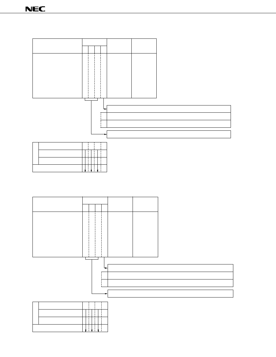
�
PD17704, 17705, 17707, 17708, 17709
120
Figure 12-3. Configuration of Serial Interface 0 Interrupt Request Register
Figure 12-4. Configuration of Timer 3 Interrupt Request Register
Name
Flag symbol
b
3
0
b
2
0
b
1
0
b
0
I
R
Q
S
I
O
0
Address
35H
Read/Write
R/W
Serial interface 0
interrupt request
Power-ON reset
WDT&SP reset
CE reset
Clock stop
0
1
Interrupt request not issued
Interrupt request issued
Indicates interrupt request issuance status of serial interface 0
Fixed to "0"
0
0
R
R
0
0
0
R: Retained
At reset
Name
Flag symbol
b
3
0
b
2
0
b
1
0
b
0
I
R
Q
T
M
3
Address
36H
Read/Write
R/W
Timer 3
interrupt request
Power-ON reset
WDT&SP reset
CE reset
Clock stop
0
1
Interrupt request not issued
Interrupt request issued
Indicates interrupt request issuance status of timer 3
Fixed to "0"
0
0
R
R
0
0
0
R: Retained
At reset

121
�
PD17704, 17705, 17707, 17708, 17709
Figure 12-5. Configuration of Timer 2 Interrupt Request Register
Figure 12-6. Configuration of Timer 1 Interrupt Request Register
Name
Flag symbol
b
3
0
b
2
0
b
1
0
b
0
I
R
Q
T
M
1
Address
38H
Read/Write
R/W
Timer 1
interrupt request
Power-ON reset
WDT&SP reset
CE reset
Clock stop
0
1
Interrupt request not issued
Interrupt request issued
Indicates interrupt request issuance status of timer 1
Fixed to "0"
0
0
R
R
0
0
0
R: Retained
At reset
Name
Flag symbol
b
3
0
b
2
0
b
1
0
b
0
I
R
Q
T
M
2
Address
37H
Read/Write
R/W
Timer 2
interrupt request
Power-ON reset
WDT&SP reset
CE reset
Clock stop
0
1
Interrupt request not issued
Interrupt request issued
Indicates interrupt request issuance status of timer 2
Fixed to "0"
0
0
R
R
0
0
0
R: Retained
At reset

�
PD17704, 17705, 17707, 17708, 17709
122
Figure 12-7. Configuration of Timer 0 Interrupt Request Register
Name
Flag symbol
b
3
0
b
2
0
b
1
0
b
0
I
R
Q
T
M
0
Address
39H
Read/Write
R/W
Timer 0
interrupt request
Power-ON reset
WDT&SP reset
CE reset
Clock stop
0
1
Interrupt request not issued
Interrupt request issued
Indicates interrupt request issuance status of timer 0
Fixed to "0"
0
0
R
R
0
0
0
R: Retained
At reset

123
�
PD17704, 17705, 17707, 17708, 17709
Figure 12-8. Configuration of INT4 Pin Interrupt Request Register
Name
Flag symbol
b
3
I
N
T
4
b
2
0
b
1
0
b
0
I
R
Q
4
Address
3AH
Read/Write
R/W
INT4 pin
interrupt request
Power-ON reset
WDT&SP reset
CE reset
Clock stop
0
1
Interrupt request not issued
Interrupt request issued
Indicates interrupt request issuance status of INT4 pin
Fixed to "0"
Low level is input
High level is input
Detects status of INT4 pin
0
1
0
0
R
R
0
0
U
U
U
U
U: Undefined, R : Retained
At reset

�
PD17704, 17705, 17707, 17708, 17709
124
Figure 12-9. Configuration of INT3 Pin Interrupt Request Register
Name
Flag symbol
b
3
I
N
T
3
b
2
0
b
1
0
b
0
I
R
Q
3
Address
3BH
Read/Write
R/W
INT3 pin
interrupt request
Power-ON reset
WDT&SP reset
CE reset
Clock stop
0
1
Interrupt request not issued
Interrupt request issued
Indicates interrupt request issuance status of INT3 pin
Fixed to "0"
Low level is input
High level is input
Detects status of INT3 pin
0
1
0
0
R
R
0
0
U
U
U
U
U: Undefined, R : Retained
At reset

125
�
PD17704, 17705, 17707, 17708, 17709
Figure 12-10. Configuration of INT2 Pin Interrupt Request Register
Name
Flag symbol
b
3
I
N
T
2
b
2
0
b
1
0
b
0
I
R
Q
2
Address
3CH
Read/Write
R/W
INT2 pin
interrupt request
Power-ON reset
WDT&SP reset
CE reset
Clock stop
0
1
Interrupt request not issued
Interrupt request issued
Indicates interrupt request issuance status of INT2 pin
Fixed to "0"
Low level is input
High level is input
Detects status of INT2 pin
0
1
0
0
R
R
0
0
U
U
U
U
U: Undefined, R : Retained
At reset
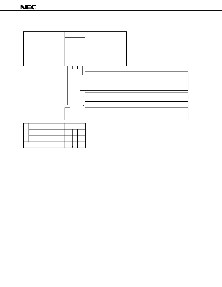
�
PD17704, 17705, 17707, 17708, 17709
126
Figure 12-11. Configuration of INT1 Pin Interrupt Request Register
Name
Flag symbol
b
3
I
N
T
1
b
2
0
b
1
0
b
0
I
R
Q
1
Address
3DH
Read/Write
R/W
INT1 pin
interrupt request
Power-ON reset
WDT&SP reset
CE reset
Clock stop
0
1
Interrupt request not issued
Interrupt request issued
Indicates interrupt request issuance status of INT1 pin
Fixed to "0"
Low level is input
High level is input
Detects status of INT1 pin
0
1
0
0
R
R
0
0
U
U
U
U
U: Undefined, R: Retained
At reset
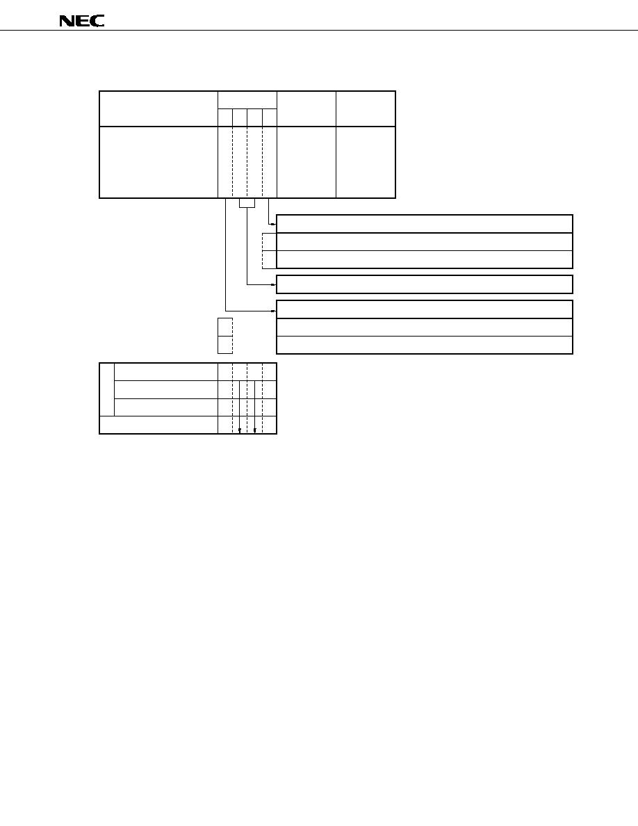
127
�
PD17704, 17705, 17707, 17708, 17709
Figure 12-12. Configuration of INT0 Pin Interrupt Request Register
Name
Flag symbol
b
3
I
N
T
0
b
2
0
b
1
0
b
0
I
R
Q
0
Address
3EH
Read/Write
R/W
INT0 pin
interrupt request
Power-ON reset
WDT&SP reset
CE reset
Clock stop
0
1
Interrupt request not issued
Interrupt request issued
Indicates interrupt request issuance status of INT0 pin
Fixed to "0"
Low level is input
High level is input
Detects status of INT0 pin
0
1
0
0
R
R
0
0
U
U
U
U
U: Undefined, R: Retained
At reset
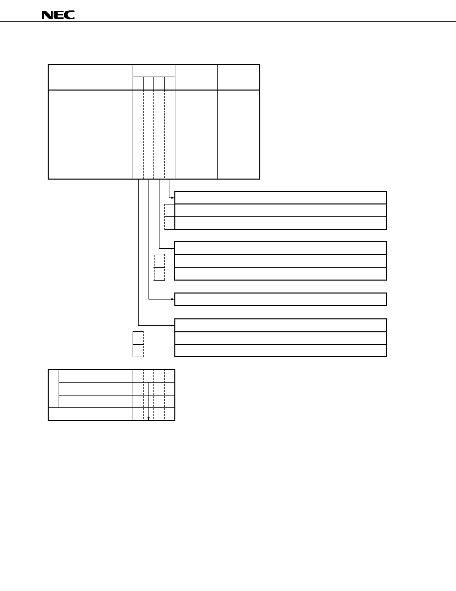
�
PD17704, 17705, 17707, 17708, 17709
128
Figure 12-13. Configuration of CE Pin Interrupt Request Register
Name
Flag symbol
b
3
C
E
b
2
0
b
1
C
E
C
N
T
S
T
T
b
0
I
R
Q
C
E
Address
3FH
Read/Write
R/W
CE pin
interrupt request
Power-ON reset
WDT&SP reset
CE reset
Clock stop
0
1
U
U
U
U
0
0
0
0
0
0
0
R
R
0
1
Interrupt request not issued
Interrupt request issued
Indicates interrupt request issuance status of CE pin
Stops
Operates
Detects status of CE reset counter
Fixed to "0"
Low level is input
High level is input
Detects status of CE pin
0
1
U : Undefined, R : Retained
At reset

129
�
PD17704, 17705, 17707, 17708, 17709
12.2.2 Function and configuration of interrupt request flag (IP
���
)
Each interrupt request flag enables the interrupt of the corresponding peripheral hardware unit.
In order for an interrupt to be accepted, all the following conditions must be satisfied.
�
The interrupt must be enabled by the corresponding interrupt request flag.
�
The interrupt request must be issued by the corresponding interrupt request flag.
�
The EI instruction (which enables all interrupts) must be executed.
The interrupt enable flags are located on the interrupt enable register on the register file.
Figures 12-14 through 12-16 show the configuration and function of each interrupt enable register.
Figure 12-14. Configuration of Interrupt Enable Register 1
Name
Flag symbol
b
3
I
P
S
I
O
1
b
2
I
P
S
I
O
0
b
1
I
P
T
M
3
b
0
I
P
T
M
2
Address
2DH
Read/Write
R/W
Interrupt enable 1
Power-ON reset
WDT&SP reset
CE reset
Clock stop
At reset
0
1
0
0
0
0
0
0
0
0
0
1
Disables
Enables
Enables or disables timer 2 interrupt
Disables
Enables
Enables or disables timer 3 interrupt
Disables
Enables
Enables or disables serial interface 0 interrupt
Disables
Enables
Enables or disables serial interface 1 interrupt
0
1
0
1
Retained
Retained

�
PD17704, 17705, 17707, 17708, 17709
130
Figure 12-15. Configuration of Interrupt Enable Register 2
Name
Flag symbol
b
3
I
P
T
M
1
b
2
I
P
T
M
0
b
1
I
P
4
b
0
I
P
3
Address
2EH
Read/Write
R/W
Interrupt enable 2
Power-ON reset
WDT&SP reset
CE reset
At reset
0
1
0
0
0
0
0
0
0
0
0
1
Disables
Enables
Enables or disables INT3 pin interrupt
Enables or disables INT4 pin interrupt
Enables or disables timer 0 interrupt
Enables or disables timer 1 interrupt
0
1
0
1
Retained
Retained
Clock stop
Disables
Enables
Disables
Enables
Disables
Enables
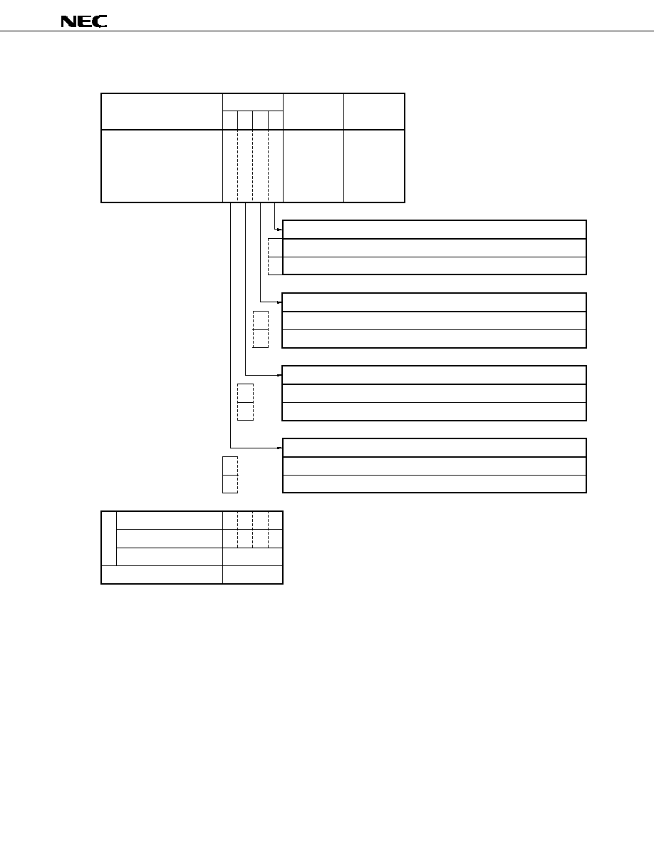
131
�
PD17704, 17705, 17707, 17708, 17709
Figure 12-16. Configuration of Interrupt Enable Register 3
Name
Flag symbol
b
3
I
P
2
b
2
I
P
1
b
1
I
P
0
b
0
I
P
C
E
Address
2FH
Read/Write
R/W
Interrupt enable 3
At reset
0
1
0
0
0
0
0
0
0
0
0
1
Enables or disables CE pin interrupt
Enables or disables INT0 pin interrupt
Enables or disables INT1 pin interrupt
Enables or disables INT2 pin interrupt
0
1
0
1
Power-ON reset
WDT&SP reset
CE reset
Disables
Enables
Retained
Retained
Clock stop
Disables
Enables
Disables
Enables
Disables
Enables
�
PD17704, 17705, 17707, 17708, 17709
132
12.2.3 Vector address generator (VAG)
The vector address generator generates a branch address (vector address) of the program memory
corresponding to an interrupt source that has been accepted from the corresponding peripheral hardware.
Table 12-1 shows the vector addresses of the respective interrupt sources.
Table 12-1. Interrupt Sources and Vector Addresses
Interrupt Source
Vector Address
Falling edge of CE pin
00CH
INT0 pin
00BH
INT1 pin
00AH
INT2 pin
009H
INT3 pin
008H
INT4 pin
007H
Timer 0
006H
Timer 1
005H
Timer 2
004H
Timer 3
003H
Serial interface 0
002H
Serial interface 1
001H
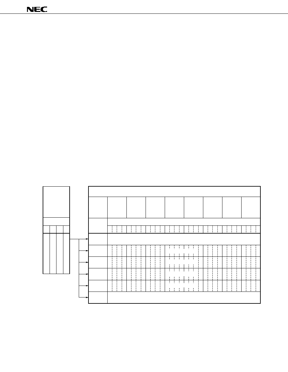
133
�
PD17704, 17705, 17707, 17708, 17709
12.3 Interrupt Stack Register
12.3.1 Configuration and function of interrupt stack register
Figure 12-17 shows the configuration of the interrupt stack register.
The interrupt stack register saves the contents of the following system registers (except the address register
(AR)) when an interrupt is accepted.
�
Window register (WR)
�
Bank register (BANK)
�
Index register (IX)
�
General pointer (RP)
�
Program status word (PSWORD)
When an interrupt is accepted and the contents of the above system registers are saved to the interrupt stack,
the contents of the above system registers, except the window register, are reset to "0".
The interrupt stack can save the contents of the above system registers at up to four levels.
Therefore, interrupts can be nested up to four levels.
The contents of the interrupt stack register are restored to the system registers when the interrupt return
(RETI) instruction is executed.
The contents of the interrupt stack register are undefined at power-ON reset.
The previous contents are retained at CE reset and on execution of the clock stop instruction.
Figure 12-17. Configuration of Interrupt Stack Register
Window
stack
WRSK
b
3
b
2
b
1
b
0
b
3
b
2
b
1
b
0
b
3
b
2
b
1
b
0
b
3
b
2
b
1
b
0
b
3
b
2
b
1
b
0
b
3
b
2
b
1
b
0
b
3
b
2
b
1
b
0
b
3
b
2
b
1
b
0
Bank
stack
BANKSK
Index
stack H
IXHSK
Index
stack M
IXHSK
Index
stack L
IXHSK
Pointer
stack H
RPHSK
Pointer
stack L
RPLSK
Status
stack
PSWSK
Bit
Undefined
Interrupt stack register (INTSK)
Name
Address
0H
1H
2H
3H
4H
5H
I N T S K 1
I N T S K 2
I N T S K 3
I N T S K 4
Interrupt stack
pointer of
system register
Bit
b
2
b
3
b
0
b
1
S
Y
S
S
P
2
0
S
Y
S
S
P
0
S
Y
S
S
P
1
Undefined

�
PD17704, 17705, 17707, 17708, 17709
134
12.3.2 Interrupt stack pointer of system register
The interrupt stack pointer of the system register detects the nesting level of interrupts. The interrupt stack
pointer can be only read and cannot be written.
The configuration and function of the interrupt stack pointer are illustrated below.
Name
Flag symbol
b
3
0
b
2
S
Y
S
R
S
P
2
b
1
S
Y
S
R
S
P
1
b
0
S
Y
S
R
S
P
0
Address
08H
Read/Write
R
Interrupt stack pointer of
system registers
0
1
1
1
0
0
0
1
1
1
Use prohibited
4 levels (INTSK1)
3 levels (INTSK2)
2 levels (INTSK3)
1 level (INTSK4)
0 level
Detects level of interrupt stack of system registers
Fixed to "0"
0
1
0
1
0
1
0
0
1
1
0
0
0
0
0
0
1
1
Power-ON reset
WDT&SP reset
CE reset
Retained
At reset
Clock stop
( )
( )
( )
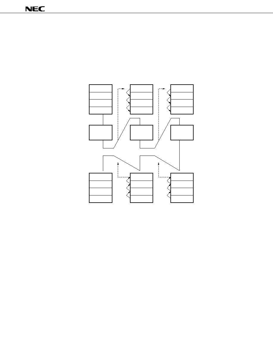
135
�
PD17704, 17705, 17707, 17708, 17709
12.3.3 Interrupt stack operation
Figure 12-8 shows the operation of the interrupt stack.
When nested interrupts exceeding four levels are accepted, since the contents saved first are discarded they
therefore must be saved by the program.
Figure 12-18. Operation of Interrupt Stack (1/2)
(a) Where interrupt nesting level is 4 or less
Undefined
Undefined
Undefined
Undefined
MAIN
Undefined
Undefined
Undefined
Undefined
MAIN
Undefined
Undefined
Undefined
A
MAIN
Undefined
Undefined
Undefined
A
MAIN
Undefined
Undefined
B
A
MAIN
Undefined
Undefined
Main routine
Interrupt A
Interrupt B
RETI
RETI
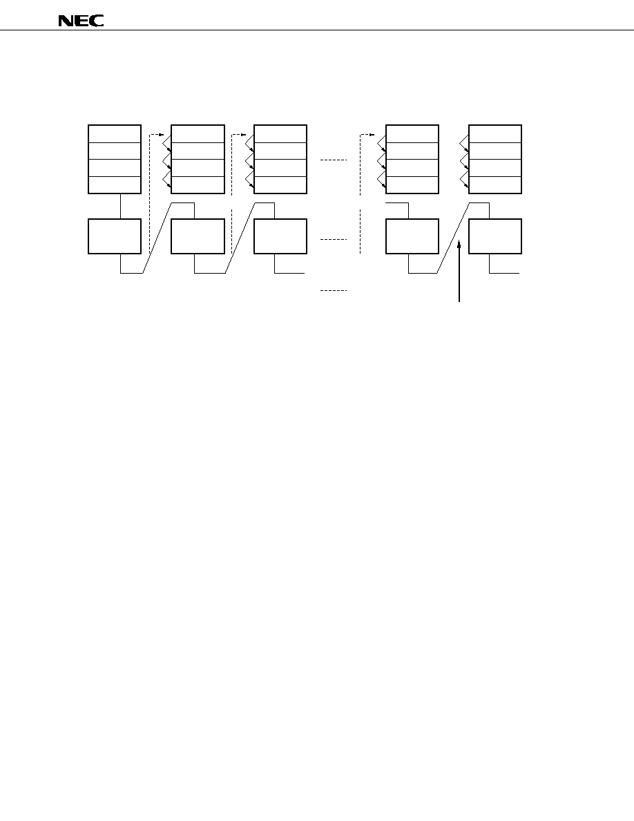
�
PD17704, 17705, 17707, 17708, 17709
136
Figure 12-18. Operation of Interrupt Stack (2/2)
(b) Where interrupt nesting level is 5 or more
Caution
The system is reset when an interrupt of level 5 is accepted.
However, the ISPRES flag, which resets the non-maskable interrupt if the interrupt stack
overflows or underflows, must be set to "1". This flag is "1" after system reset, and can then
be written only once.
Undefined
Undefined
MAIN
MAIN
Undefined
Undefined
Undefined
A
A
MAIN
Undefined
Undefined
B
Main routine
Interrupt level 1
Interrupt level 2
C
B
A
MAIN
D
D
C
B
A
E
Interrupt D
Interrupt E
Interrupt level 4
Interrupt level 5
System reset
Interrupt A
Interrupt C

137
�
PD17704, 17705, 17707, 17708, 17709
12.4 Stack Pointer, Address Stack Registers, and Program Counter
The address stack registers save a return address when execution returns from an interrupt routine.
The stack pointer specifies the address of an address stack register.
When an interrupt is accepted, the value of the stack pointer is decremented by one, and the value of the
program counter at that time is saved to an address stack register specified by the stack pointer.
Next, the interrupt routine is executed. When the interrupt return (RETI) instruction is executed after that,
the contents of an address stack register specified by the stack pointer are restored to the program counter,
and the value of the stack pointer is incremented by one.
For further information, also refer to 3. ADDRESS STACK (ASK).
12.5 Interrupt Enable Flip-Flop (INTE)
The interrupt enable flip-flop enables or disables the 12 types of maskable interrupts.
When this flip-flop is set, all the interrupts are enabled. When it is reset, all the interrupts are disabled.
This flip-flop is set or reset by dedicated instructions EI (to set) and DI (to reset).
The EI instruction sets this flip-flop when the instruction next to EI is executed, and the DI instruction resets
the flip-flop while it is being executed.
When an interrupt is accepted, this flip-flop is automatically reset.
This flip-flop is also reset at power-ON reset, at a reset by the RESET pin, at a watchdog timer, overflow or
underflow of the stack, and at CE reset. The flip-flop retains the previous status on execution of the clock stop
instruction.

�
PD17704, 17705, 17707, 17708, 17709
138
12.6 Accepting Interrupt
12.6.1 Accepting interrupt and priority
The following operations are performed before an interrupt is accepted.
(1) Each peripheral hardware unit outputs an interrupt request signal to the corresponding interrupt request
block if a given interrupt condition (for example, input of the falling signal to the INT0 pin) is satisfied.
(2) When each interrupt request block accepts an interrupt request signal from the corresponding peripheral
hardware unit, it sets the corresponding interrupt request flag (for example, IRQ0 flag if it is the INT0 pin
that has issued the interrupt request) to "1".
(3) The interrupt enable flag corresponding to each interrupt request flag (for example, IP0 flag if the interrupt
request flag is IRQ0) is set to "1" when each interrupt request flag is set to "1", and each interrupt request
block outputs "1".
(4) The signal output by the interrupt request block is ORed with the output of the interrupt enable flip-flop,
and an interrupt accept signal is output.
This interrupt enable flip-flop is set to "1" by the EI instruction, and reset to "0" by the DI instruction.
If "1" is output by each interrupt request processing block while the interrupt enable flip-flop is set to "1",
the interrupt is accepted.
As shown in Figure 12-1, the output of the interrupt enable flip-flop is input to each interrupt request block
via an AND circuit when an interrupt is accepted.
The signal input to each interrupt request block causes the interrupt request flag corresponding to each
interrupt request flag to be reset to "0" and the vector address corresponding to each interrupt to be output.
If the interrupt request block outputs "1" at this time, the interrupt accept signal is not transferred to the next
stage. If two or more interrupt requests are issued at the same time, therefore, the interrupts are accepted
according to the priority shown in Table 12-2.
Unless the interrupt request enable flag is set to "1", the corresponding interrupt is not accepted.
Therefore, by resetting the interrupt enable flag to "0", the interrupt with a high hardware priority can be
disabled.
Table 12-2. Interrupt Priority
Interrupt Source
Priority
Falling edge of CE pin
1
INT0 pin
2
INT1 pin
3
INT2 pin
4
INT3 pin
5
INT4 pin
6
Timer 0
7
Timer 1
8
Timer 2
9
Timer 3
10
Serial interface 0
11
Serial interface 1
12

139
�
PD17704, 17705, 17707, 17708, 17709
12.6.2 Timing chart when interrupt is accepted
The timing charts in Figure 12-19 illustrate the operations performed when an interrupt or interrupts are
accepted.
Figure 12-19 (1) is the timing chart when one interrupt is accepted.
(a) in (1) is the timing chart where the interrupt request flag is set to "1" after all the others, and (b) is the
timing chart where the interrupt enable flag is set to "1" after all the others.
In either case, the interrupt is accepted when the interrupt request flag, interrupt enable-flip flop, and interrupt
enable flag all have been set to "1".
If the flag or flip-flop that has been set last is set in the first instruction cycle of the "MOVT DBF, @AR"
instruction or by an instruction that satisfies a given skip condition, the interrupt is accepted in the second
instruction cycle of the "MOVT DBF, @AR" instruction or after the instruction that is skipped (this instruction
is treated as NOP) has been executed.
The interrupt enable flip-flop is set in the instruction cycle next to that in which the EI instruction is executed.
Therefore, the interrupt is accepted after the instruction next to the EI instruction has been executed even
when the interrupt request flag is set in the execution cycle of the EI instruction.
(2) in Figure 12-19 is the timing chart where two or more interrupts are used.
When two or more interrupts are used, the interrupts are accepted according to the hardware priority if all
the interrupt enable flags are set. However, the hardware priority can be changed by setting the interrupt enable
flags by the program.
"Instruction cycle" shown in Figure 12-19 is a special cycle in which the interrupt request flag is reset, a vector
address is specified, and the contents of the program counter are saved after an interrupt has been accepted.
It takes 1.78
�
s, which is equivalent to one instruction execution time, to be completed.
For details, refer to 12.7 Operation after Interrupt Has Been Accepted.

�
PD17704, 17705, 17707, 17708, 17709
140
Figure 12-19. Timing Charts When Interrupt Is Accepted (1/3)
(1) When one interrupt (e.g., rising of INT0 pin) is used
(a) If there is no interrupt mask time by the interrupt flag (IP
���
)
<1> If a normal instruction which is not "MOVT" or an instruction that satisfies a skip
condition is executed when interrupt is accepted
<2> If "MOVT" or an instruction that satisfies a skip condition is executed when interrupt is
accepted
Instruction
EI
MOV
WR, #0010B
POKE
INTPM3, WR
MOVT DBF,
@AR or skip
instruction
Interrupt
cycle
INTE
1.78 s
Interrupt enable period
INT0 pin interrupt accepted
INT0 pin interrupt service
INT0 pin
IRQ0 flag
IP0 flag
1 instruction
cycle
�
Instruction
EI
MOV
WR, #0010B
POKE
INTPM3, WR
Normal
instruction
Interrupt
cycle
INTE
INT0 pin
IRQ0 flag
IP0 flag
1 instruction
cycle
1.78 s
Interrupt enable period
INT0 pin interrupt accepted
INT0 pin interrupt service
�
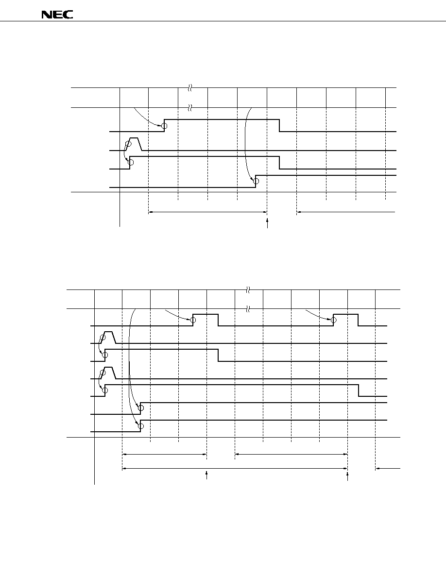
141
�
PD17704, 17705, 17707, 17708, 17709
Figure 12-19. Timing Charts When Interrupt Is Accepted (2/3)
(b) If interrupt is kept pending by the interrupt enable flag
(2) If two or more interrupts (e.g., INT0 pin and INT1 pin) are used
(a) Hardware priority
Instruction
EI
MOV
WR, #0010B
POKE
INTPM3, WR
Interrupt
cycle
INTE
INT0 pin
IRQ0 flag
IP0 flag
INT0 pin interrupt pending period
INT0 pin interrupt accepted
INT0 pin interrupt service
Instruction
EI
MOV
WR, #0110B
POKE
INTPM3, WR
Interrupt
cycle
INTE
INT0 pin
IRQ0 flag
INT1 pin
INT0 pin interrupt pending period
INT0 pin interrupt accepted
INT0 pin interrupt service
EI
Interrupt
cycle
IRQ1 flag
IP0 flag
IP1 flag
INT1 pin interrupt pending period
INT1 pin
interrupt service
INT1 pin interrupt accepted

�
PD17704, 17705, 17707, 17708, 17709
142
Figure 12-19. Timing Charts When Interrupt Is Accepted (3/3)
(b) Software priority
Instruction
EI
MOV
WR, #0100B
POKE
INTPM3, WR
Interrupt
cycle
INTE
INT0 pin
IRQ0 flag
INT1 pin
INT1 pin interrupt pending period
INT1 pin interrupt accepted
INT1 pin interrupt service
EI
Interrupt
cycle
IRQ1 flag
IP0 flag
IP1 flag
INT0 pin interrupt pending period
INT0 pin
interrupt service
INT0 pin interrupt accepted
MOV
WR, #0110B
POKE
INTPM3, WR

143
�
PD17704, 17705, 17707, 17708, 17709
12.7 Operations after Interrupt Has Been Accepted
When an interrupt is accepted, the following operations are sequentially performed automatically.
(1) The interrupt enable flip-flop and the interrupt request flag corresponding to the accepted interrupt
request are reset to "0". As a result, the other interrupts are disabled.
(2) The contents of the stack pointer are decremented by one.
(3) The contents of the program counter are saved to an address stack register specified by the stack pointer.
At this time, the contents of the program counter are the program memory address after the address at
which the interrupt has been accepted.
For example, if a branch instruction is executed when the interrupt has been accepted, the contents of
the program counter are the branch destination address. If a subroutine call instruction is executed, the
contents of the program counter are the call destination address. If the skip condition of a skip instruction
is satisfied, the next instruction is executed as NOP and then the interrupt is accepted. Consequently,
the contents of the program counter are the address after that of the instruction that is skipped.
(4) The contents of the system registers (except the address register) are saved to the interrupt stack.
(5) The contents of the vector address generator corresponding to the interrupt that has been accepted are
transferred to the program counter. In other words, execution branches to the interrupt routine.
The operations (1) through (5) above require the time of one special instruction cycle (1.78
�
s) in which normal
instruction execution is not performed.
This instruction cycle is called an "interrupt cycle".
In other words, the time of one instruction cycle (1.78
�
s) is required after an interrupt has been accepted
until execution branches to the corresponding vector address.
12.8 Returning from Interrupt Routine
The interrupt return (RETI) instruction is used to return from an interrupt routine to the processing during
which an interrupt was accepted.
When the RETI instruction is executed, the following operations are sequentially performed automatically.
(1) The contents of an address stack register specified by the stack pointer are restored to the program
counter.
(2) The contents of the interrupt stack are restored to the system registers.
(3) The contents of the stack pointer are incremented by one.
The operations (1) through (3) above require one instruction cycle (1.78
�
s) in which the RETI instruction
is executed.
The only difference between the RETI instruction and the RET and RETSK instructions, which are subroutine
return instructions, is the restoration of the bank register and index register in step (2) above.

�
PD17704, 17705, 17707, 17708, 17709
144
12.9 External Interrupts (CE and INT0 through INT4 pins)
12.9.1 Outline of external interrupts
Figure 19-20 outlines the external interrupts.
As shown in the figure, external interrupt requests are issued at the rising or falling edges of signals input
to the INT0 through INT4 pins, and at the falling edge of the CE pin.
Whether an interrupt request is issued at the rising or falling edge of an INT pin is independently specified
by the program.
The INT0 through INT4 and CE pins are Schmitt trigger input pins to prevent malfunctioning due to noise.
These pins do not accept a pulse input of less than 100 ns.
Figure 12-20. Outline of External Interrupts
INT0
INT0 flag
IEG0 flag
Edge detection
block
Schmitt trigger
IRQ0 flag
INT1
INT1 flag
IEG1 flag
Edge detection
block
Schmitt trigger
IRQ1 flag
INT2
INT2 flag
IEG2 flag
Edge detection
block
Schmitt trigger
IRQ2 flag
INT3
INT3 flag
IEG3 flag
Edge detection
block
Schmitt trigger
IRQ3 flag
INT4
INT4 flag
IEG4 flag
Edge detection
block
Schmitt trigger
IRQ4 flag
CE
CE flag
Edge detection
block
Schmitt trigger
IRQCE flag
INT4SEL
INT3SEL
Interrupt control block
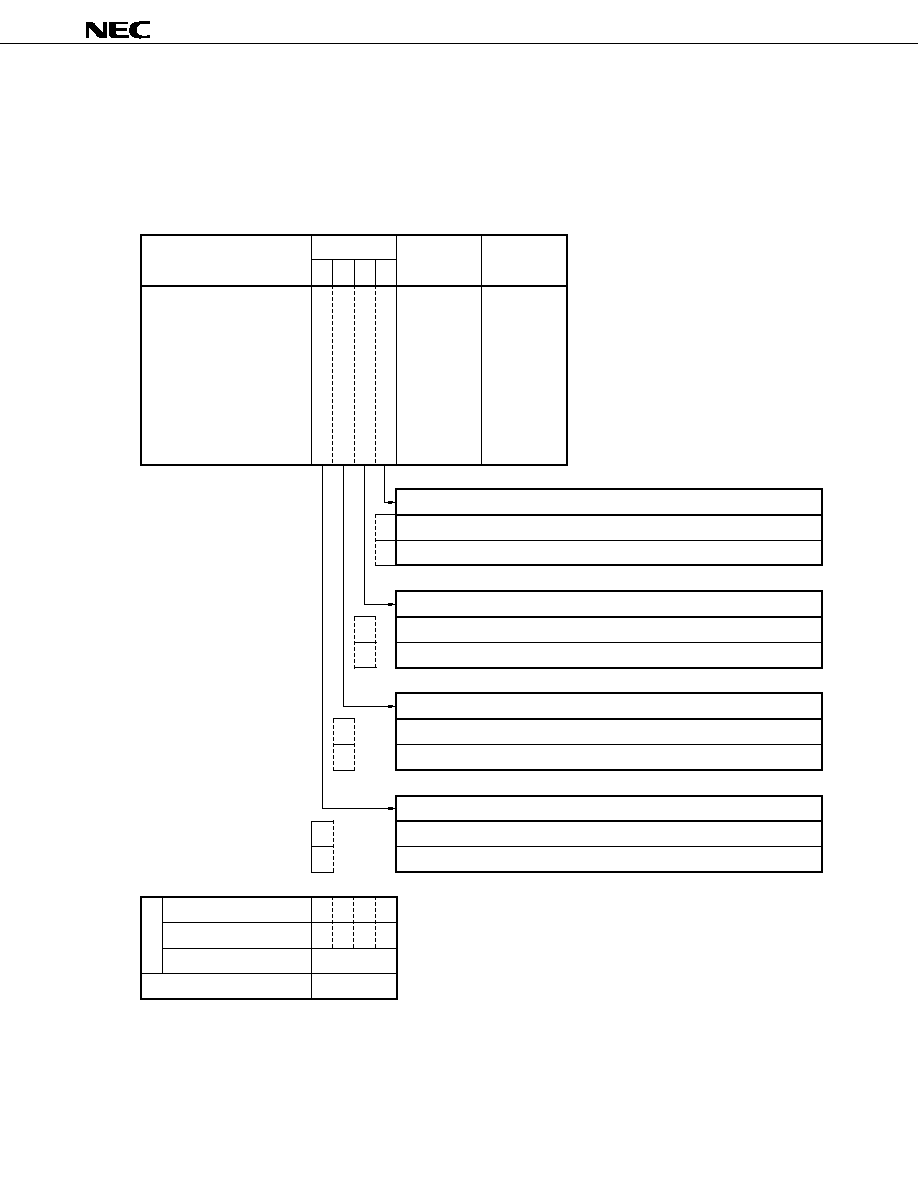
145
�
PD17704, 17705, 17707, 17708, 17709
12.9.2 Edge detection block
The edge detection block specifies the valid edge (rising or falling edge) of an input signal that issues the
interrupt request of INT0 to INT4 pins, by using an interrupt edge selection register.
Figure 12-21 shows the configuration and function of the interrupt edge selection register.
Figure 12-21. Configuration of Interrupt Edge Selection Register (1/2)
Caution
The external input delays about 100 ns.
Name
Flag symbol
b
3
I
E
G
4
b
2
I
N
T
4
S
E
L
b
1
I
E
G
3
b
0
I
N
T
3
S
E
L
Address
1EH
Read/Write
R/W
Interrupt edge selection 1
Power-ON reset
WDT&SP reset
CE reset
Clock stop
At resat
0
1
0
0
0
0
0
0
0
0
0
1
Interrupt pin (edge detection cricuit operates)
General-purpose port pin (edge detection cricuit stops)
Selects function of P1A2/INT3 pin
Rising edge
Falling edge
Selects input edge to issue interrupt request (INT3 pin)
Interrupt pin (edge detection cricuit operates)
General-purpose port pin (edge detection cricuit stops)
Selects function of P1A3/INT4 pin
Rising edge
Falling edge
Selects input edge to issue interrupt request (INT4 pin)
0
1
0
1
Retained
Retained
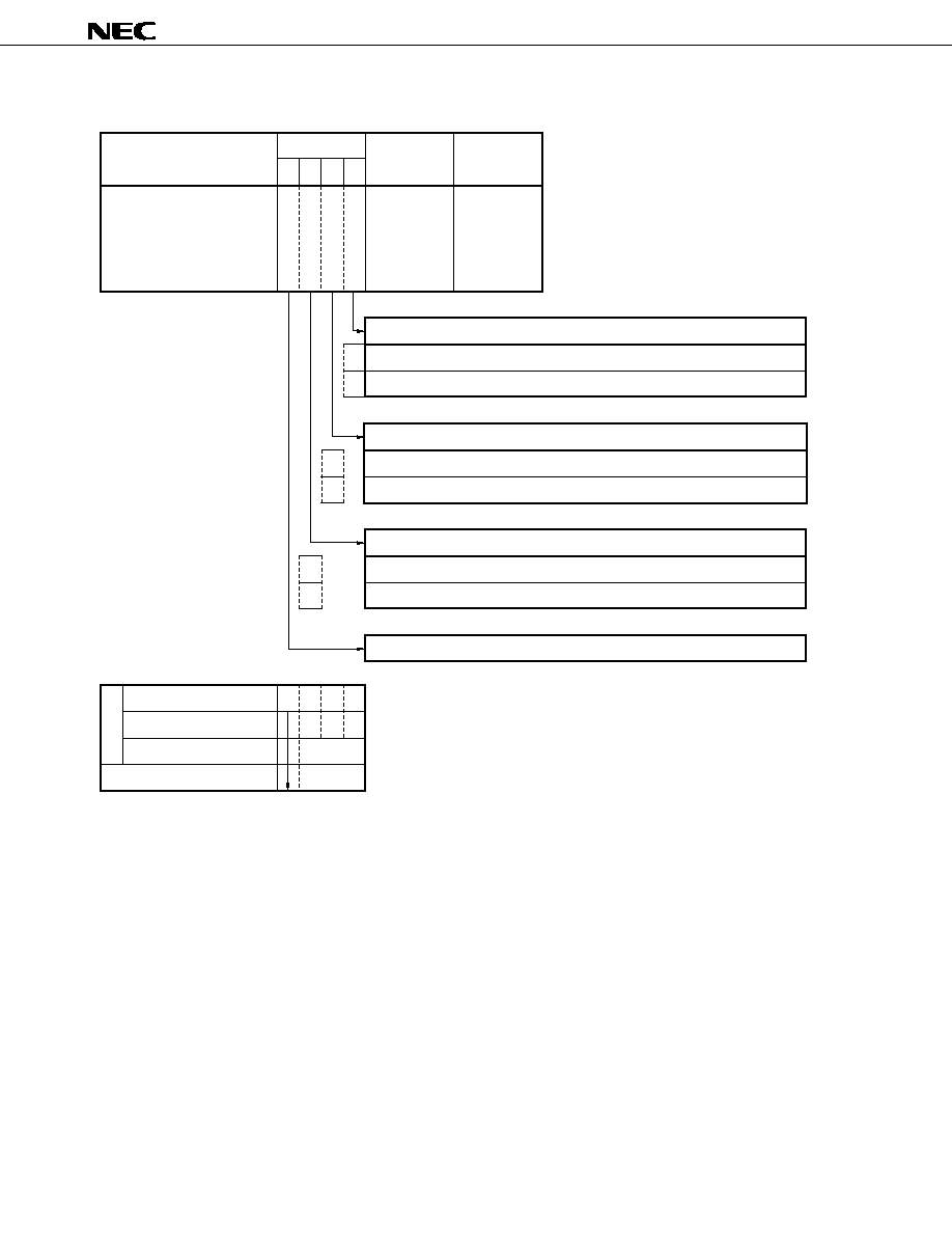
�
PD17704, 17705, 17707, 17708, 17709
146
Figure 12-21. Configuration of Interrupt Edge Selection Register (2/2)
Caution
The external input is delayed about 100 ns.
Note that an interrupt request signal may be issued at the time when the interrupt request issuance edge is
switched by the interrupt edge selection flags (IEG0 through IEG4).
As indicated in the table 12-3, for example, if the IEG0 flag is set to "1" (falling edge), the high level is input
from the INT0 pin and the IEG0 flag is reset to "0", the edge detection circuit judges that the rising edge is input
and an interrupt request is issued.
Name
Flag symbol
b
3
0
b
2
I
E
G
2
b
1
I
E
G
1
b
0
I
E
G
0
Address
1FH
Read/Write
R/W
Interrupt edge selection 2
Power-ON reset
WDT&SP reset
CE reset
Clock stop
At resat
0
0
0
0
0
0
0
0
1
Rising edge
Falling edge
Selects input edge to issue interrupt request (INT0 pin)
Rising edge
Falling edge
Selects input edge to issue interrupt request (INT1 pin)
Rising edge
Falling edge
Selects input edge to issue interrupt request (INT2 pin)
Fixed to "0"
0
1
0
1
Retained
Retained

147
�
PD17704, 17705, 17707, 17708, 17709
Table 12-3. Issuance of Interrupt Request by Changing IEG Flag
Changes in IEG0 through IEG4 Flags Status of INT0 through INT4 Pins
Issuance of Interrupt Request
Status of Interrupt Request Flag
1
0
Low level
Not issued
Retains previous status
(Falling) (Rising)
High level
Issued
Set to "1"
0
1
Low level
Issued
Set to "1"
(Rising) (Falling)
High level
Not issued
Retains previous status
12.9.3 Interrupt control block
The signal levels that are input to the INT0 through INT4 pins can be detected by using the INT0 through INT4
flags.
Because these flags are reset independently of interrupts, when the interrupt function is not used the INT0
through INT2 pins can be used as a 3-bit input port, and P1A2/INT3 and P1A3/INT4 pins can be used as a 2-
bit general-purpose input port.
If the interrupts are not enabled, these ports can be used as general-purpose port pins whose rising or falling
edge can be detected by reading the corresponding interrupt request flags.
At this time, however, the interrupt request flags are not automatically reset and must be reset by the program.
For further information, also refer to 12.2.1 Configuration and function of interrupt request flag (IRQ
���
).
12.10 Internal Interrupts
The following six internal interrupts are available.
�
Timer 0
�
Timer 1
�
Timer 2
�
Timer 3
�
Serial interface 0
�
Serial interface 1
12.10.1 Timer 0, timer 1, timer 2, and timer 3 interrupts
Interrupt requests are issued at fixed intervals.
For details, refer to 13. TIMER.
12.10.2 Serial interface 0 and serial interface 1 interrupts
Interrupt requests can be issued at the end of a serial output or serial input operation.
For details, refer to 16. SERIAL INTERFACE.

�
PD17704, 17705, 17707, 17708, 17709
148
13. TIMERS
Timers are used to manage the program execution time.
13.1 Outline of Timers
Figure 13-1 outlines the timers.
The following five timers are available.
�
Basic timer 0
�
Timer 0
�
Timer 1
�
Timer 2
�
Timer 3
Basic timer 0 detects the status of a flip-flop that is set at fixed time intervals in software.
Timers 0 through 3 are modulo timers and can use interrupts.
Basic timer 0 can also be used to detect a power failure. Timer 3 is multiplexed with the D/A converter.
The clock of each timer is created by dividing the system clock (4.5 MHz).
Figure 13-1. Outline of Timers (1/2)
(1) Basic timer 0
(2) Timer 0
(3) Timer 1
Clock selection
4.5 MHz
BTM0CY flag
Flip-flop
Clock selection
4.5 MHz
Gate control
TM0G
Start/stop
8-bit counter
Interrupt control
Coincidence detection
Overflow
Modulo register
Clock selection
4.5 MHz
Start/stop
8-bit counter
Interrupt control
Coincidence detection
Modulo register

149
�
PD17704, 17705, 17707, 17708, 17709
Figure 13-1. Outline of Timers (2/2)
(4) Timer 2
(5) Timer 3
Clock selection
4.5 MHz
Start/stop
8-bit counter
Interrupt control
Coincidence detection
Modulo register
Clock divider
4.5 MHz
Start/stop
Interrupt control
Coincidence detection
Multiplexed whih D/A converter
Modulo register
8-bit counter or
9-bit counter

�
PD17704, 17705, 17707, 17708, 17709
150
13.2 Basic Timer 0
13.2.1 Outline of basic timer 0
Figure 13-2 outlines basic timer 0.
Basic timer 0 is used as a timer by detecting in software the BTM0CY flag that is set at fixed intervals (100,
50, 20, or 10 ms).
If the BTM0CY flag is read first after power-ON reset, "0" is always read. After that, the flag is set to "1" at
fixed intervals.
If the CE pin goes high, CE reset is effected in synchronization with the timing at which the BTM0CY flag is
set next.
Therefore, a power failure can be detected by reading the content of the BTM0CY flag at system reset (power-
ON reset or CE reset).
For the details of power failure detection, refer to 21. RESET.
Figure 13-2. Outline of Basic Timer 0
Remarks 1. BTM0CK1 and BTM0CK0 (bits 1 and 0 of basic timer 0 clock selection register: refer to Figure
13-3) set the time intervals at which the BTM0CY flag is set.
2. BTM0CY (bit 0 of basic timer 0 carry register: refer to Figure 13-4) detects the status of the
flip-flop.
Divider
Clock selection block
4.5 MHz
BTM0CY flag
Selector
BTM0CK0 flag
BTM0CK1 flag
Flip-flop

151
�
PD17704, 17705, 17707, 17708, 17709
13.2.2 Clock selection block
The clock selection block divides the system clock (4.5 MHz) and sets the time interval at which the BTM0CY
flag is to be set, by using the BTM0CK0 and BTM0CK1 flags.
Figure 13-3 shows the configuration of the basic timer 0 clock selection register.
Figure 13-3. Configuration of Basic Timer 0 Clock Selection Register
Name
Flag symbol
b
3
0
b
2
0
b
1
B
T
M
0
C
K
1
b
0
B
T
M
0
C
K
0
Address
18H
Read/Write
R/W
Basic timer 0 clock selection
Power-ON reset
WDT&SP reset
CE reset
Clock stop
At reset
0
1
0
1
0
0
10 Hz (100 ms)
20 Hz (50 ms)
50 Hz (20 ms)
100 Hz (10 ms)
Fixed to "0"
Sets time interval at which BTM0CY flag is set
0
0
0
0
1
1
0
0
Retained
Retained

�
PD17704, 17705, 17707, 17708, 17709
152
13.2.3 Flip-flop and BTM0CY flag
The flip-flop is set at fixed intervals and its status is detected by the BTM0CY flag of the basic timer 0 carry
register.
When the BTM0CY flag is read, it is reset to "0" (Read & Reset).
The BTM0CY flag is "0" at power-ON reset, and is "1" at CE reset and on execution of the clock stop
instruction. Therefore, this flag can be used to detect a power failure.
The BTM0CY flag is not set after power application until an instruction that reads it is executed. Once the
read instruction has been executed, the flag is set at fixed intervals.
Figure 13-4 shows the configuration of the basic timer 0 carry register.
Figure 13-4. Configuration of Basic Timer 0 Carry Register
Name
Flag symbol
b
3
0
b
2
0
b
1
0
b
0
B
T
M
0
C
Y
Address
17H
Read/Write
R & Reset
Basic timer 0 carry
Power-ON reset
WDT&SP reset
CE reset
R: Retained
Clock stop
At reset
0
1
0
R
1
R
Flip-flop is not set
Flip-flop is set
Fixed to "0"
Detects status of flip-flop
0
0
0

153
�
PD17704, 17705, 17707, 17708, 17709
13.2.4 Example of using basic timer 0
An example of a program using basic timer 0 is shown below.
This program executes processing A every 1 second.
Example
CLR2
BTM0CK1, BTM0CK0
; Sets BTM0CY flag setting pulse to 10 Hz (100 ms)
MOV
M1, #0
LOOP:
SKT1
BTM0CY
; Branches to NEXT if BTM0CY flag is "0"
BR
NEXT
ADD
M1, #1
; Adds 1 to M1
SKE
M1, #0AH
; Executes processing A if M1 is "10" (1 second has elapsed)
BR
NEXT
MOV
M1, #0
Processing A
NEXT:
Processing B
; Executes processing B and branches to LOOP
BR
LOOP
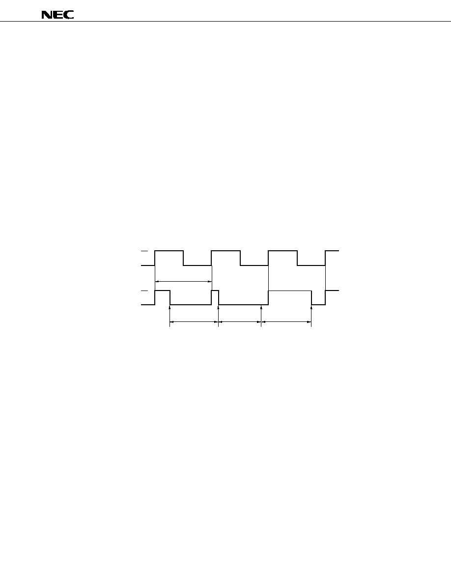
�
PD17704, 17705, 17707, 17708, 17709
154
13.2.5 Errors of basic timer 0
Errors of basic timer 0 include an error due to the detection time of the BTM0CY flag, and an error that occurs
when the time interval at which the BTM0CY flag is to be set is changed.
The following paragraphs (1) and (2) describe each error.
(1) Error due to detection time of BTM0CY flag
The time to detect the BTM0CY flag must be shorter than the time at which the BTM0CY flag is set (refer
to 13.2.6 Notes on using basic timer 0).
Where the time interval at which the BTM0CY flag is detected is t
CHECK
and the time interval at which the
flag is set is t
SET
(100, 50, 20, or 10 ms), t
CHECK
and t
SET
must relate as follows.
t
CHECK
< t
SET
At this time, the error of the timer when the BTM0CY flag is detected is as follows, as shown in Figure
13-5.
0 < Error < t
SET
Figure 13-5. Error of Basic Timer 0 due to Detection Time of BTM0CY Flag
As shown in Figure 13-5, the timer is updated because BTM0CY flag is "1" when it is detected in step
<2>.
When the flag is detected next in step <3>, it is "0". Therefore, the timer is not updated until the flag is
detected again in <4>.
This means that the timer is extended by the time of t
CHECK3
.
H
L
BTM0CY flag
setting pulse
t
SET
t
CHECK1
SKT1
BTM0CY
<1>
SKT1
BTM0CY
<2>
SKT1
BTM0CY
<3>
SKT1
BTM0CY
<4>
t
CHECK2
t
CHECK3
1
0
BTM0CY flag
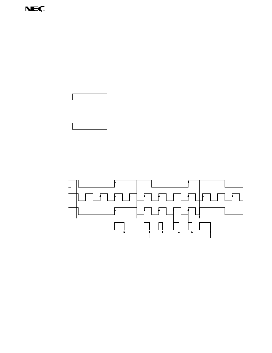
155
�
PD17704, 17705, 17707, 17708, 17709
(2) Error when time interval to set BTM0CY flag is changed
The BTM0CK1 and BTM0CK0 flags set the time of the BTM0CY flag.
As described in 13.2.2, four types of timer time-setting pulses can be selected: 10 Hz, 20 Hz, 50 Hz, and
100 Hz.
At this time, these four pulses operate independently. If the timer time-setting pulse is changed by using
the BTM0CK1 and BTM0CK0 flags, an error occurs as described in the example below.
Example
; <1>
INTIFLG NOT BTM0CK1, NOT BTM0CK0 ; Sets BTM0CY flag setting pulse to 10 Hz
(100 ms)
Processing A
; <2>
INITFLG BTM0CK1, NOT BTM0CK0
; Sets BTM0CY flag setting pulse to 50 Hz
(20 ms)
Processing A
; <3>
INITFLG NOT BTM0CK1, NOT BTM0CK0 ; Sets BTM0CY flag setting pulse to 10 Hz
(100 ms)
At this time, the BTM0CY flag setting pulse is changed as shown in Figure 13-6.
Figure 13-6. Changing BTM0CY Flag Setting Pulse
As shown in Figure 13-6, if the BTM0CY flag setting time is changed and the new pulse falls, the BTM0CY
flag retains the previous status (<2> in the figure). If the new pulse rises, however, the BTM0CY flag
is set to "1" (<3> in the figure).
Although changing the pulse setting between 10 Hz (100 ms) and 50 Hz (20 ms) is described in this
example, the same applies to changing the pulse in respect to 20 Hz (50 ms) and 100 Hz (10 ms).
H
L
Internal pulse
10 HZ
Internal pulse
50 HZ
H
L
BTM0CY flag
1
0
BTM0CY flag
setting pulse
H
L
SKT1 BTM0CY
<2>
<3>
<1>

�
PD17704, 17705, 17707, 17708, 17709
156
Therefore, as shown in Figure 13-7, the error of the time until the BTM0CY flag is first set after the
BTM0CY flag setting time has been changed is as follows:
�t
SET
< Error < t
CHECK
t
SET
: new setting time of BTM0CY flag
t
CHECK
: time to detect BTM0CY flag
Phase differences are provided among the internal pules of 10, 20, 50, and 100 Hz. Because these phase
differences are shorter than the newly set pulse time, they are included in the above error.
Figure 13-7. Timer Error When BTM0CY Flag Setting Time Is Changed from A to B
H
L
H
L
H
L
H
L
t
SET
SKT1 BTM0CY
Intrinsic timer time
Actual timer time
Time changed
Internal pulse A
Internal pulse B
BTM0CY flag
setting pulse
BTM0CY flag
t
SET
t
CHECK
Actual timer time
Intrinsic timer time
Time changed
An error of t
CHECK
occurs if the timer time is
changed immediately after BTM0CY flag
has been detected because the flag is then
reset once.
An error of -t
SET
occurs if BTM0CY flag is
detected immediately after the timer time
has been changed because the flag then
becomes "1".

157
�
PD17704, 17705, 17707, 17708, 17709
13.2.6 Cautions on using basic timer 0
(1) BTM0CY flag detection time interval
Keep the time to detect the BTM0CY flag shorter than the time at which the BTM0CY flag is set.
This is because, if the time of processing B is longer than the time interval at which the BTM0CY flag
is set as shown in Figure 13-8, setting of the BTM0CY flag is overlooked.
Figure 13-8. BTM0CY Flag Detection and BTM0CY Flag
(2) Timer updating processing time and BTM0CY flag detection time interval
As described in (1) above, time interval t
SET
at which the BTM0CY flag is detected must be shorter than
the time for which to set the BTM0CY flag.
At this time, even if the time interval at which the BTM0CY flag is detected is short, if the updating
processing time of the timer is long the processing of the timer may not be executed normally at CE reset.
Therefore, the following condition must be satisfied.
t
CHECK
+ t
TIMER
< t
SET
t
CHECK
: time to detect BTM0CY flag
t
TIMER
: timer updating processing time
t
SET
: time to set BTM0CY flag
An example is given below.
H
BTM0CY flag
setting pulse
BTM0CY flag
L
SKT1 BTM0CY SKT1 BTM0CY
Processing A
Processing B
SKT1 BTM0CY
t
SET
<1>
<2>
<3>
<4>
<5>
1
0
Because execution time of processing B takes too long
after detection of BTM0CY flag that has been set to "1"
in <2>, BTM0CY flag that is set to "1" in <3> cannot be
detected.

�
PD17704, 17705, 17707, 17708, 17709
158
Example Example of timer updating processing and BTM0CY flag detection time interval
START:
CLR2
BTM0CK1, BTM0CK0
; Sets BTM0CY flag setting pulse to 10 Hz (100 ms)
BTIMER:
; <1>
SKT1
BTM0CY
; Updates timer if BTM0CY flag is "1"
BR
AAA
Timer updating
BR
BTIMER
AAA:
Processing A
BR
BTIMER
The timing chart of the above program is shown below.
(3) Compensating basic timer 0 carry at CE reset
Next, an example of compensating the timer at CE reset is described below.
As shown in the example below, the timer must be compensated at CE reset "if the BTM0CY flag is used
for power failure detection and if the BTM0CY flag is used for a watch timer".
The BTM0CY flag is reset (to 0) first on power application (power-ON reset), and is disabled from being
set until it is read once by the "PEEK" instruction.
If the CE pin goes high, CE reset is effected in synchronization with the rising edge of the BTM0CY flag
setting pulse. At this time, the BTM0CY flag is set (to 1) and the timer is started.
By detecting the status of the BTM0CY flag at system reset (power-ON reset or CE reset), therefore, it
can be identified whether a power-ON reset or CE reset has been effected (power failure detection). That
is, power-ON reset has been effected if the flag is "0", and CE reset has been effected if it is "1".
At this time, the watch timer must continue operating even if CE reset has been effected.
However, because the BTM0CY flag is reset to 0 when it is read to detect a power failure, the set status
(1) of the BTM0CY flag is overlooked once. If the delay function of CE reset is used, the value set to
the CE reset timer carry counter (control register address 06H) is overlooked.
Consequently, the watch timer must be updated if CE reset is identified by means of power failure
detection.
For the details of power failure detection, refer to 21. RESET.
t
SET
H
CE pin
BTM0CY detection interval
t
CHECK
Timer updating processing
t
TIMER
BTM0CY flag
BTM0CY flag
setting pulse
L
H
L
1
<1> SKT1
BTM0CY
<2> SKT1
BTM0CY
CE reset
0
If this timer updating processing
time is too long, CE reset is effected
during processing.

159
�
PD17704, 17705, 17707, 17708, 17709
Example Example of compensating timer at CE reset (to detect power failure and update watch timer
using BTM0CY flag)
START:
; Program address 0000H
Processing A
; <1>
SKT1
BTM0CY
; Embedded macro
; Tests BTM0CY flag
BR
INITIAL
; if "0", branches to INITIAL (power failure detection)
BACKUP:
; <2>
100-ms watch updating
; Compensates watch timer because of backup (CE reset)
; Initial value "1" is stored as CE reset timer carry
; counter value
LOOP:
; <3>
Processing B
: While performing processing B,
SKF1
BTM0CY
; tests BTM0CY flag and updates watch timer
BR
BACKUP
BR
LOOP
INITIAL:
CLR2
BTM0CK1, BTM0CK0
; Embedded macro
; Because power failure (power-ON reset) occurs,
; sets setting time of BTM0CY flag to 100 ms, and
; executes processing C
Processing C
BR
LOOP
Figure 13-9 shows the timing chart of the above program.
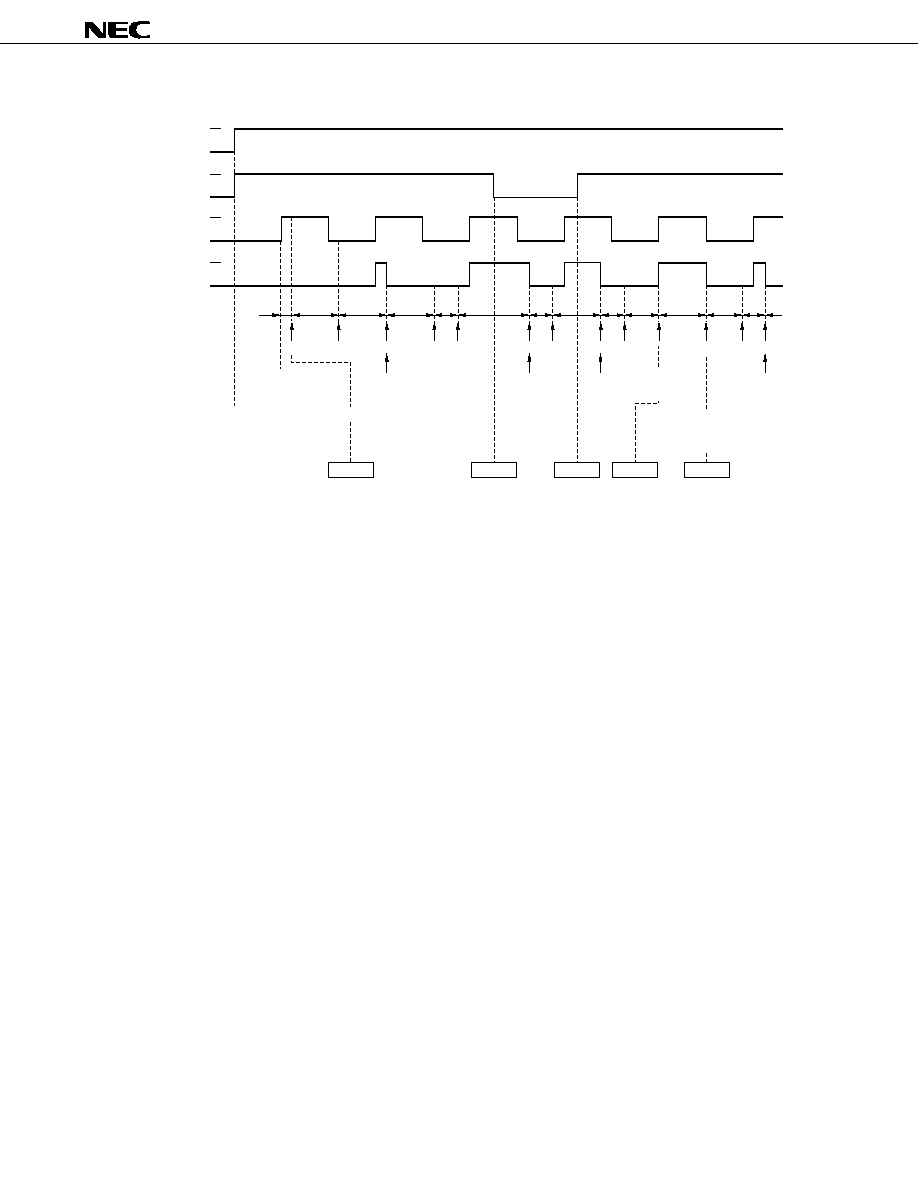
�
PD17704, 17705, 17707, 17708, 17709
160
Figure 13-9. Timing Chart
As shown in Figure 13-9, the program is started from address 0000H because the internal 10-Hz pulse
rises when supply voltage V
DD
is first applied.
When the BTM0CY flag is detected at point A, it is judged that the BTM0CY flag is reset (to 0) and that
a power failure (power-ON reset) has occurred because the power has just been applied.
Therefore, "processing C" is executed, and the BTM0CY flag setting pulse is set to 100 ms.
Because the content of the BTM0CY flag is read once at point A, the BTM0CY flag will be set to 1 every
100 ms.
Next, even if the CE pin goes low at point B and high at point C, the program counts up the watch timer
while executing "processing B", unless the clock stop instruction is executed.
At point C, because the CE pin goes high, CE reset is effected at point D at which the BTM0CY flag setting
pulse rises next time, and the program is started from address 0000H.
When the BTM0CY flag is detected at point E at this time, it is set to 1. Therefore, this is judged to be
a back up (CE reset).
As is evident from the above figure, unless the watch is updated by 100 ms at point E, the watch is delayed
by 100 ms each time CE reset is effected.
If processing A takes longer than 100 ms when a power failure is detected at point E, the setting of the
BTM0CY flag is overlooked two times. Therefore, processing A must be completed within 100 ms.
The above description also applies when the BTM0CY flag setting pulse is set to 50, 20, or 10 ms.
Therefore, the BTM0CY flag must be detected for power failure detection within the BTM0CY flag setting
time after the program has been started from address 0000H.
A
Power-ON reset
Start from address 0
CE reset
Start from address 0
Application of
supply voltage
BTM0CY flag detected
C
5 V
V
DD
CE
BTM0CY flag setting
pulse (10 Hz)
BTM0CY flag
Program processing
Program instruction
0 V
H
L
H
L
1
0
B
B
B
B
B
B
B
B
B
B
<3>
Watch UP
<3>
Watch UP
<3>
Watch UP
<3>
<3>
<1>
Watch UP
<3>
<3>
<3>
<3>
<3>
<1>
A
Updates watch timer because
setting of BTM0CY flag (to 1)
is detected
Point A
Point B
Point C
Point D
Point E

161
�
PD17704, 17705, 17707, 17708, 17709
(4) If BTM0CY flag is detected at the same time as CE reset
As described in (3) above, CE reset is effected as soon as the BTM0CY flag is set to 1.
If the instruction that reads the BTM0CY flag happens to be executed at the same time as CE reset at
this time, the BTM0CY flag reading instruction takes precedence.
Therefore, if the next setting the BTM0CY flag (rising of BTM0CY flag setting pulse) after the CE pin has
gone high coincides with execution of the BTM0CY flag reading instruction, CE reset is effected at "the
next timing at which the BTM0CY flag is set".
This operation is illustrated in Figure 13-10.
Figure 13-10. Operation When CE Reset Coincides with BTM0CY Flag Reading Instruction
Consequently, if the BTM0CY flag detection time interval coincides with the BTM0CY flag setting time
in a program that cyclically detects the BTM0CY flag, CE reset is never effected.
Therefore, the following point must be noted.
Because one instruction cycle is 1.78
�
s (1/562.5 kHz), a program that detects the BTM0CY flag once,
say, every 1125 instructions, reads the BTM0CY flag every 1.78
�
s
�
1125 = 2 ms.
Because the timer time setting pulse is 100 ms at this time, if setting and detection of the BTM0CY flag
coincide once, CE reset is never effected.
H
BTM0CY flag
setting pulse
BTM0CY flag
CE pin
L
H
L
1.78 s
SKT1 BTM0CY
(PEEK ���)
SKT1
BTM0CY
CE reset
(SKT ���)
1
0
H
BTM0CY flag
setting pulse
BTM0CY flag
Instruction
Embedded macro
PEEK WR, . MF. BTM0CY SHR 4
SKT WR, #. DF. BTM0CY AND 000FH
L
1
0
If BTM0CY flag is read at this time, CE reset is
effected delayed once.
Originally, program is started from address 0000H here.
However, CE reset is not effected because it happens to
coincide with program that reads BTM0CY flag.
SKT1
BTM0CY
�

�
PD17704, 17705, 17707, 17708, 17709
162
Therefore, do not create a cyclic program that satisfies the following condition.
t
SET
�
1125
= n (n: natural number)
X
t
SET
: B TM0CY flag setting time
X
: Cycle X step of instruction that reads BTM0CY flag
An example of a program that satisfies the above condition is shown below. Do not create such a
program.
Example
Processing A
CLR2
BTM0CK1, BTM0CK0
; Embedded macro
; Sets BTM0CY flag setting pulse to 100 ms
LOOP:
; <1>
SKT1
BTM0CY
; Embedded macro
BR
BBB
AAA:
1121 steps
BR
LOOP
BBB:
1121 steps
BR
LOOP
Because the BTM0CY flag reading instruction in <1> is repeatedly executed every 1125 instruction in
this example, CE reset is not effected if the BTM0CY flag happens to be set at the timing of instruction
in <1>.
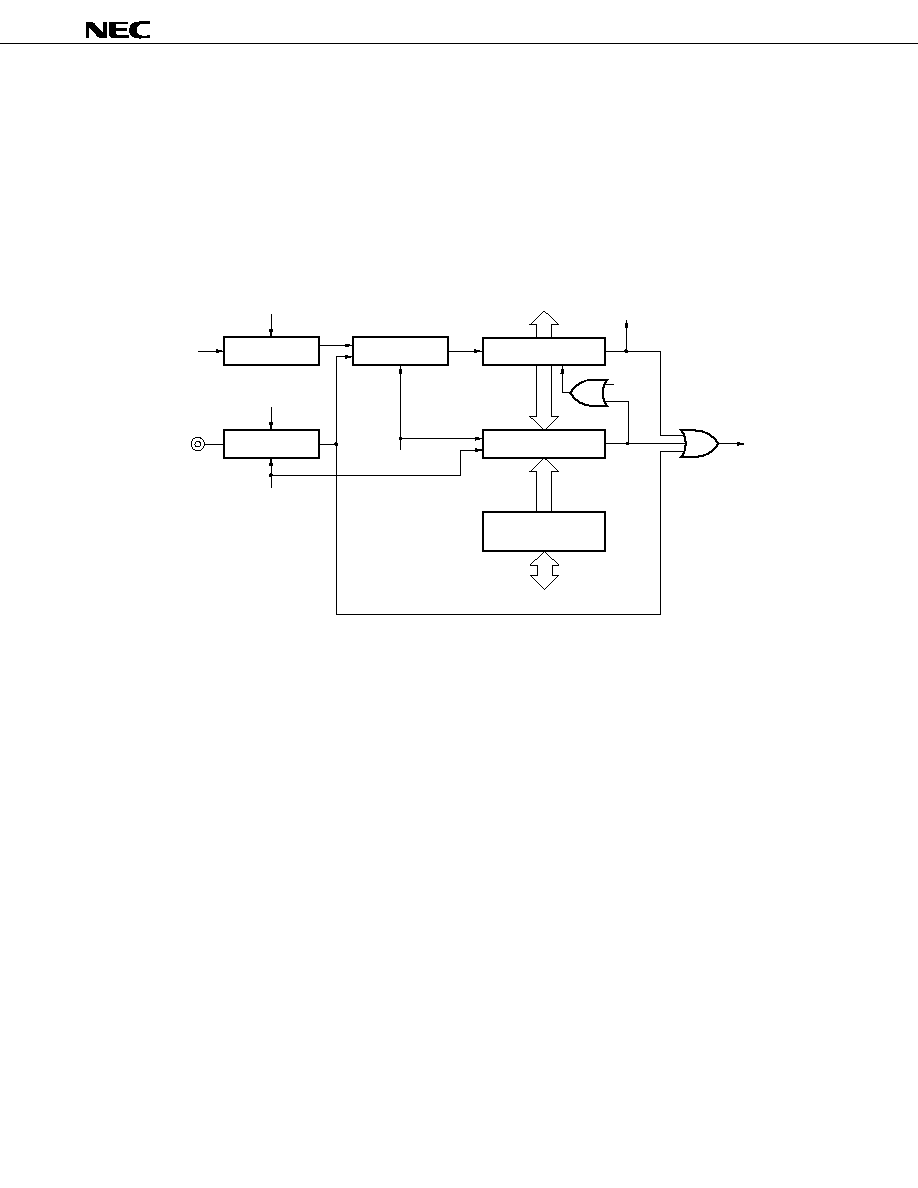
163
�
PD17704, 17705, 17707, 17708, 17709
13.3 Timer 0
13.3.1 Outline of timer 0
Figure 13-11 shows the outline of timer 0.
The timer 0 is used as timer (modulo mode) by comparing the count value with the previously set value after
the basic clock (100 kHz, 10 kHz, 2 kHz, and 1 kHz) has counted by the 8-bit counter.
The pulse width of the signal input from the TM0G pin can be measured (external gate counter).
Figure 13-11. Outlines Timer 0
Remarks 1. TM0CK1 and TM0CK0 (bits 1 and 0 of timer 0 counter clock selection register: refer to Figure
13-13) set a basic clock frequency.
2. TM0MD (bit 0 of timer 0 mode selection register: refer to Figure 13-14) selects the modulo
counter and gate counter.
3. TM0GOEG (bit 1 of timer 0 mode selection register: refer to Figure 13-14) sets the open edge
of an external gate.
4. TM0GCEG (bit 2 of timer 0 mode selection register: refer to Figure 13-14) sets the close edge
of an external gate.
5. TM0OVF (bit 3 of timer 0 mode selection register: refer to Figure 13-14) detects an overflow
of timer 0 counter.
6. TM0RES (bit 2 of timer 0 counter clock selection register: refer to Figure 13-13) resets timer
0 counter.
Clock selection
4.5 MHz
Gate control
P1A0/TM0G
Start/stop
Timer 0 counter (TM0C)
TM0CK1 flag
TM0CK0 flag
TM0GCEG flag
TM0GOEG flag
TM0MD flag
TM0MD flag
Coincidence detection circuit
8
TM0RES
flag
DBF
Gate closed
Overflow
Sets IRQTM0 flag
TM0OVF flag
DBF
8
Timer 0 modulo register
(TM0M)
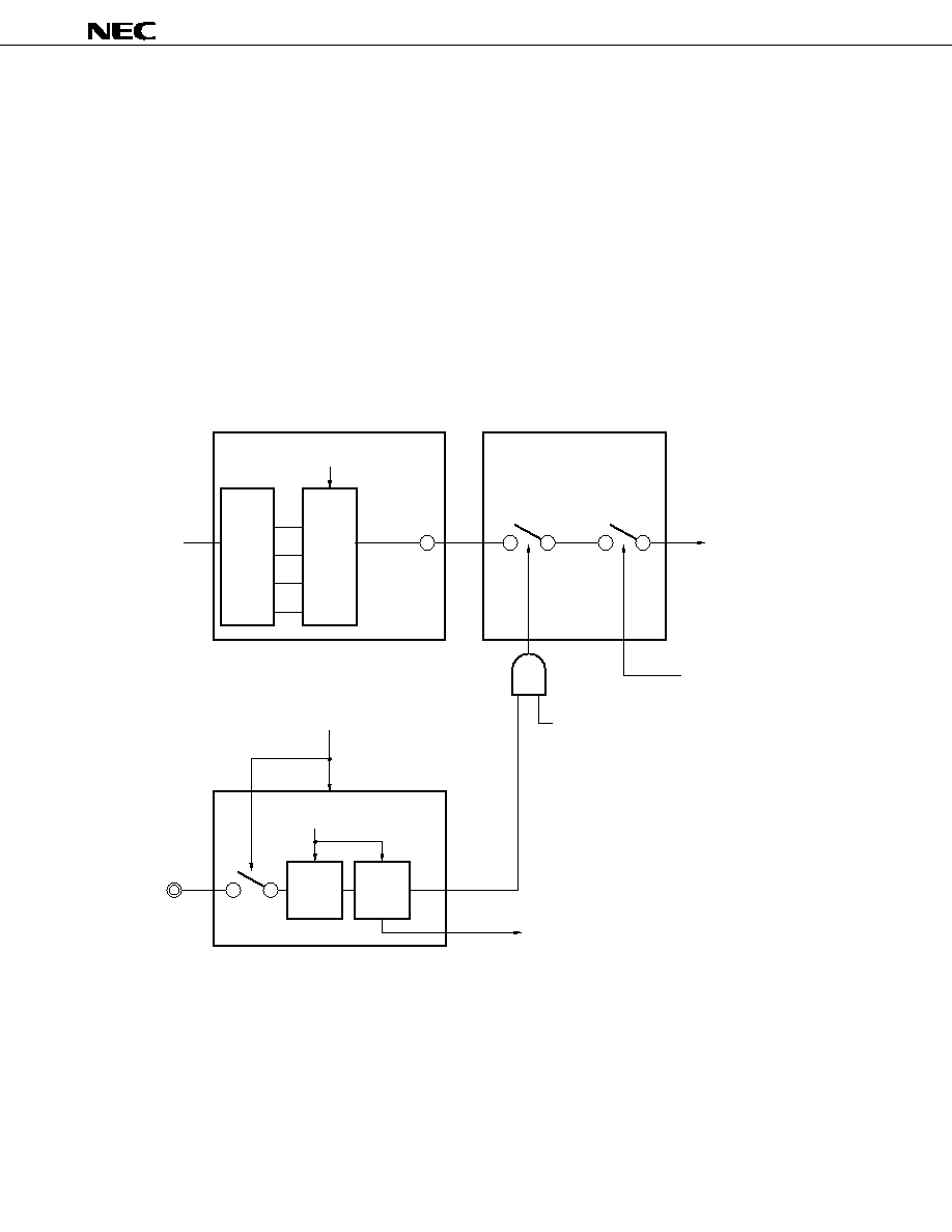
�
PD17704, 17705, 17707, 17708, 17709
164
13.3.2 Clock selection, start/stop control, and gate control blocks
Figure 13-12 shows the configuration of these blocks.
The clock selection block selects a basic clock to operate timer 0 counter.
Four types of basic clocks can be selected by using the TM0CK1 and TM0CK0 flags.
Figure 13-13 shows the configuration and function of each flag.
The start/stop block controls the TM0MD flag and open/close signal from the gate control block, and starts
or stops the basic clock to be input to timer 0 counter by the TM0EN flag.
The gate control block sets the opening or closing conditions of the gate.
It sets whether the gate is opened or closed by a rising or falling of the input signal, by using the TM0GOEG
and TM0GCEG flags. This block also issues an interrupt request when the closing condition of the gate is
detected.
Figure 13-14 shows the configuration and function of each flag.
Figure 13-12. Configuration of Clock Selection, Start/Stop Control, and Gate Control Blocks
Selector
100 kHz
10 kHz
2 kHz
1 kHz
TM0CK1
TM0CK0
Clock selection
Divider
4.5 MHz
Start/stop
Timer 0 counter
TM0EN flag
TM0MD flag
TM0MD flag
P1A0/TM0G
TM0GOEG
TM0GCEG
Gate control
Open/
close
Edge
detection
Timer 0 interrupt

165
�
PD17704, 17705, 17707, 17708, 17709
Figure 13-13. Configuration of Timer 0 Counter Clock Selection Register
Caution
When the TM0RES flag is read, 0 is always read.
Name
Flag symbol
b
3
T
M
0
E
N
b
2
T
M
0
R
E
S
b
1
T
M
0
C
K
1
b
0
T
M
0
C
K
0
Address
2BH
Read/Write
R/W
Timer 0 counter
clock selection
Power-ON reset
WDT&SP reset
CE reset
Clock stop
At reset
0
1
0
1
0
0
0
100 kHz (10 s)
10 kHz (100 s)
2 kHz (500 s)
1 kHz (1 ms)
Sets basic clock of timer 0 counter
0
0
0
0
0
0
0
0
1
1
Does not change
Resets counter
Resets timer 0 counter
0
1
0
0
0
Retained
Stops
Starts
Starts or stops timer 0
0
1
�
�
�
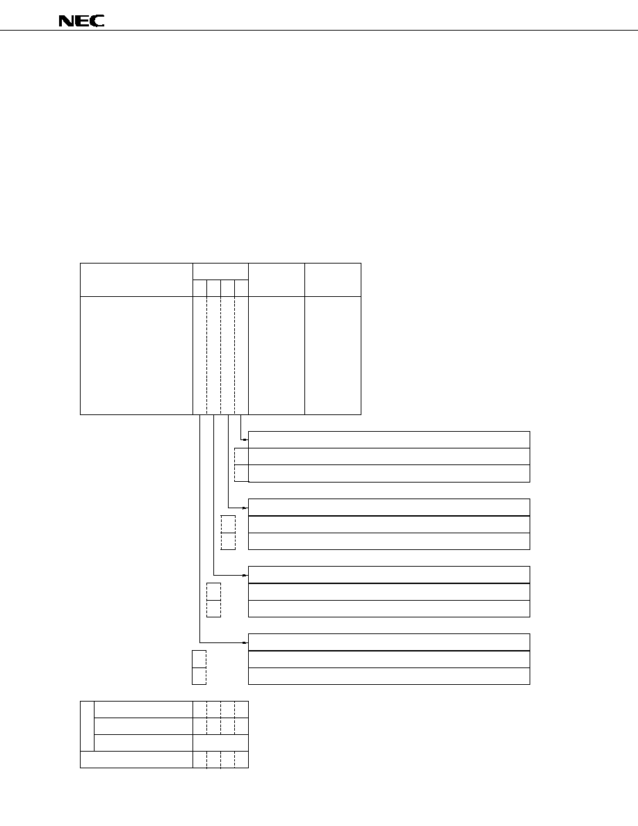
�
PD17704, 17705, 17707, 17708, 17709
166
13.3.3 Count block
The count block counts the basic clock with an 8-bit timer 0 counter, reads the count value, and issues an
interrupt request if the value of the timer 0 modulo register coincides with its value.
Timer 0 counter can be reset by the TM0RES flag.
The TM0OVF flag can detect an overflow of the counter. When an overflow occurs, an interrupt request can
be issued.
The value of the timer 0 counter can be read via data buffer.
The value of the timer 0 modulo register can be written or read via data buffer.
Figure 13-14 shows the configuration of the timer 0 mode selection register.
Figure 13-15 shows the configuration of the timer 0 counter.
Figure 13-16 shows the configuration of the timer 0 modulo register.
Figure 13-14. Configuration of Timer 0 Mode Selection Register
Name
Flag symbol
b
3
T
M
0
O
V
F
b
2
T
M
0
G
C
E
G
b
1
T
M
0
G
O
E
G
b
0
T
M
0
M
D
Address
2CH
Read/Write
R/W
Timer 0 mode selection
Power-ON reset
WDT&SP reset
CE reset
Clock stop
At reset
0
1
0
0
0
Modulo counter
Gate counter
Selects modulo counter or gate counter of timer 0
0
0
0
0
0
0
Rising edge
Falling edge
Rising edge
Falling edge
Specifies edge of gate open input signal
0
1
0
0
0
Retained
Specifies edge of gate close input signal
0
1
No overflow
Overflow
Detects timer 0 overflow
0
1
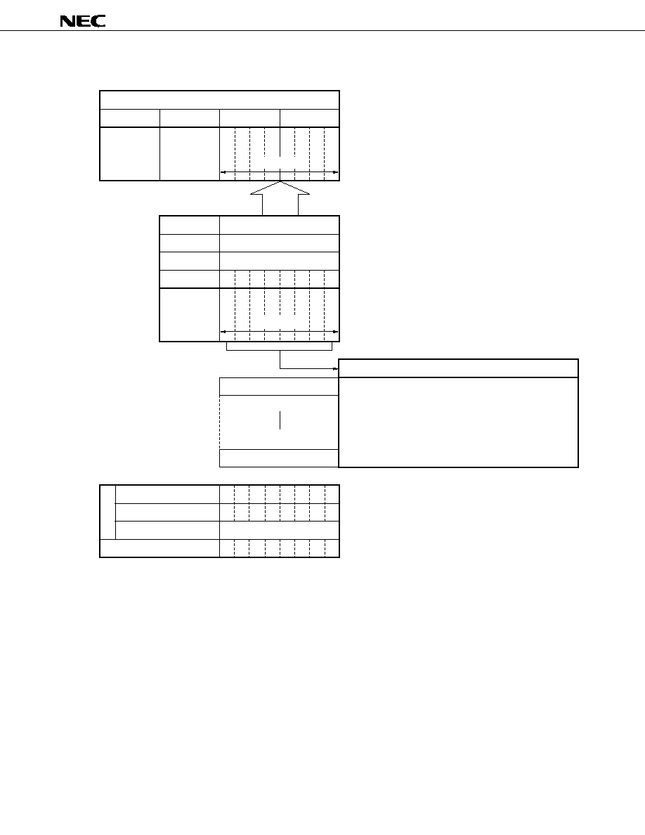
167
�
PD17704, 17705, 17707, 17708, 17709
Figure 13-15. Configuration of Timer 0 Counter
Reads count value of timer 0
Data buffer
DBF3
Don't care
DBF2
Don't care
Name
Symbol
Address
Bit
Data
DBF1
DBF0
b
3
b
2
b
1
b
0
b
7
b
6
b
5
b
4
Timer 0 counter
TM0C
1BH
Power-ON reset
WDT&SP reset
CE reset
Clock stop
0
0
0
0
0
0
0
0
0
0
0
0
0
0
0
0
0
0
0
0
0
0
0
0
Retained
Transfer data
Valid data
0
� Modulo mode
Reset if count value of timer 0 coincides with value of
modulo counter.
� External gate mode
Resets counting to 00H if overflow occurs
0FFH
8 bits
GET
PUT must not be executed
At reset
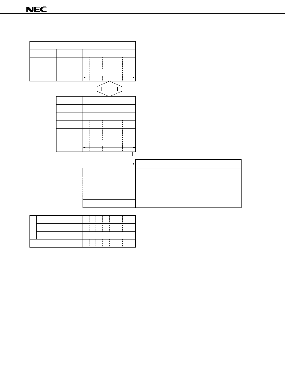
�
PD17704, 17705, 17707, 17708, 17709
168
Figure 13-16. Configuration of Timer 0 Modulo Register
Sets modulo data of timer 0
Data buffer
DBF3
Don't care
DBF2
Don't care
Name
Symbol
Address
Bit
Data
DBF1
DBF0
b
3
b
2
b
1
b
0
b
7
b
6
b
5
b
4
Timer 0 modulo register
TM0M
1AH
Power-ON reset
WDT&SP reset
CE reset
Clock stop
At reset
1
1
1
1
1
1
1
1
1
1
1
1
1
1
1
1
1
1
1
1
1
1
1
1
Retained
Transfer data
Valid data
0
� Modulo mode
Issues interrupt request when value of modulo counter
coincides with count value of timer 0.
� External gate mode
Does not issue interrupt request when value of modulo
counter coincides with count value of timer 0.
0FFH
8 bits
GET
PUT

169
�
PD17704, 17705, 17707, 17708, 17709
13.3.4 Example of using timer 0
(1) Modulo counter mode
The modulo counter mode is used for time management by generating timer 0 interrupt at fixed intervals.
An example of a program is shown below.
This program executes processing B every 500
�
s.
TM0DATA
DAT
0032H
; MODULO DATA = 50
START:
BR
INITIAL
; Reset address
; Interrupt vector address
NOP
; SIO1
NOP
; SIO0
NOP
; TM3
NOP
; TM2
NOP
; TM1
BR
INT_TM0
; TM0
NOP
; INT4
NOP
; INT3
NOP
; INT2
NOP
; INT1
NOP
; INT0
NOP
; Down edge of CE
INITIAL:
INITFLG
NOT TM0EN, TM0RES, NOT TM0CK1, NOT TM0CK0
;
(Stop) , (Reset) , (Basic clock = 10
�
s)
CLR1
TM0MD
; Modulo mode
MOV
DBF0, #(TM0MDATA SHR 0) AND 0FH
MOV
DBF1, #(TM0MDATA SHR 4) AND 0FH
PUT
TM0M, DBF
; Sets count data
SET1
IPTM0
; Enables timer 0 interrupt
EI
SET1
TM0EN
; Starts timer 0
LOOP:
Processing A
BR
LOOP
INT_TM0:
Processing B
; Timer 0 interrupt service
EI
RETI
; Return

�
PD17704, 17705, 17707, 17708, 17709
170
(2) Gate counter mode
The gate counter mode is used to count the width of a pulse input to the TM0G pin.
An example of a program is shown below.
In this program example, the width of the pulse input to the TM0G pin is counted from the falling edge
to the falling edge.
If the pulse width is 800 to 1200
�
s, processing C is executed; otherwise, processing B is executed.
If the pulse width is 2560
�
s or more, processing D is executed.
TM0800
DAT
0050H
; Count data = 80
TM01200
DAT
0078H
; Count data = 120
START:
BR
INITIAL
; Reset address
; Interrupt vector address
NOP
; SIO1
NOP
; SIO0
NOP
; TM3
NOP
; TM2
NOP
; TM1
BR
INT_TM0
; TM0
NOP
; INT4
NOP
; INT3
NOP
; INT2
NOP
; INT1
NOP
; INT0
NOP
; Down edge of CE
INITIAL:
INITFLG
NOT TM0EN, TM0RES, NOT TM0CK1, NOT TM0CK0
;
(Stop) , (Reset) , (Basic clock = 10
�
s)
INITFLG
TM0GCEG , TM0GOEG , TM0MD
;
(Falling close), (Falling open), (Gate counter)
SET1
TM0EN
; START
SET1
IPTM0
; Enables timer 0 interrupt
EI
LOOP:
Processing A
BR
LOOP
INT_TM0:
PUT
DBFSTK, DBF
; Saves data buffer
GET
DBF, TM0C
INITFLG
TM0EN, TM0RES
SKT1
TM0OVF
; Detects overflow status (2560
�
s or more?)
BR
AAA
Processing D
BR
EI_RETI
AAA:
SUB
DBF0, #TM0800 AND 0FH
SUBC
DBF1, #TM0800 SHR4 AND 0FH
SKF1
CY
; 800
�
s or more?
BR
BBB
SUB
DBF0, #TM01200 AND 0FH

171
�
PD17704, 17705, 17707, 17708, 17709
SUBC
DBF1, #TM01200 SHR4 AND 0FH
SKT1
CY
; 1200
�
s or more?
BR
BBB
Processing C
BR
EI_RETI
BBB:
Processing B
EI_RETI:
GET
DBF, DBFSTK
; Restores data buffer
EI
RETI
; Return
END
13.3.5 Error of timer 0
Timer 0 has an error of up to 1 basic clock in the following cases.
(1) On starting/stopping counter
The counter is started or stopped by ANDing the open/close condition of the gate and TM0EN flag setting
condition.
Therefore, an error of 0 to +1 clocks occurs when the gate is opened or the TM0EN flag is set, and an
error of �1 to 0 clocks occurs when the gate is closed or the flag is reset.
In all, an error of
�
1 count occurs.
(2) On resetting counter operation
An error of 0 to +1 clocks occurs when the counter is reset.
(3) On selecting basic clock during counter operation
An error of 0 to +1 clocks of the newly selected clock occurs.
13.3.6 Cautions on using timer 0
Timer 0 interrupt may occur simultaneously with the other timer interrupts and CE reset. If it is necessary
to update the timer at CE reset, do not use timer 0, use basic timer 0 instead.

�
PD17704, 17705, 17707, 17708, 17709
172
13.4 Timer 1
13.4.1 Outline of timer 1
Figure 13-17 outlines timer 1.
Timer 1 counts the basic clock (100, 10, 2, or 1 kHz) with an 8-bit counter, and compares the count value
with a value set in advance.
Figure 13-17. Outline of Timer 1
Remarks 1. TM1CK1 and TM1CK0 (bits 1 and 0 of timer 1 counter clock selection register: refer to Figure
13-18) set the basic clock frequency.
2. TM1EN (bit 3 of timer 1 counter clock selection register: refer to Figure 13-18) starts or stops
timer 1.
3. TM1RES (bit 2 of timer 1 counter clock selection register: refer to Figure 13-18) resets timer
1 counter.
Clock selection
4.5 MHz
Start/stop
Timre 1 counter (TM1C)
TM1CK1 flag
TM1CK0 flag
TM1EN flag
Coincidence detection circuit
TM1RES flag
DBF
Timer 1
IRQTM1 flag
Interrupt control
DBF
Timer 1 modulo register
(TM1M)

173
�
PD17704, 17705, 17707, 17708, 17709
13.4.2 Clock selection and start/stop control blocks
The clock selection block selects a basic clock to operate timer 1 counter.
Four types of basic clocks can be selected by using the TM1CK1 and TM1CK0 flags.
The start/stop block starts or stops the basic clock input to timer 1 by using the TM1EN flag.
Figure 13-18 shows the configuration and function of each flag.
13.4.3 Count block
The count block counts the basic clock with timer 1 counter, reads the count value, and issues an interrupt
request when its count value coincides with the value of the timer 1 modulo register.
The timer 1 counter can be reset by the TM1RES flag.
The timer 1 counter is automatically reset when its value coincides with the value of the timer 1 modulo
register.
The value of the timer 1 counter can be read via data buffer.
Data can be written to the value of the timer 1 modulo register via data buffer.
Figure 13-18 shows the configuration of timer 1 counter clock selection register.
Figure 13-19 shows the configuration of the timer 1 counter.
Figure 13-20 shows the configuration of the timer 1 modulo register.

�
PD17704, 17705, 17707, 17708, 17709
174
Figure 13-18. Configuration of Timer 1 Counter Clock Selection Register
Caution
When the TM1RES flag is read, 0 is always read.
Name
Flag symbol
b
3
T
M
1
E
N
b
2
T
M
1
R
E
S
b
1
T
M
1
C
K
1
b
0
T
M
1
C
K
0
Address
2AH
Read/Write
R/W
Timer 1 counter clock selection
Power-On reset
WDT&SP reset
CE reset
Clock stop
At reset
0
1
0
1
0
0
0
100 kHz (10 s)
10 kHz (100 s)
2 kHz (500 s)
1 kHz (1 ms)
Sets basic clock of timer 1 counter
0
0
0
0
0
0
0
0
1
1
Does not change
Resets counter
Resets timer 1 counter (valid on writing)
0
1
0
0
0
Retained
Stops
Starts
Starts or stops timer 1
0
1
�
�
�

175
�
PD17704, 17705, 17707, 17708, 17709
Figure 13-19. Configuration of Timer 1 Counter
Reads count value of timer 1
Data buffer
DBF3
Don't care
DBF2
Don't care
Name
Symbol
Address
Bit
Data
DBF1
DBF0
b
3
b
2
b
1
b
0
b
7
b
6
b
5
b
4
Timer 1 counter
TM1C
1DH
Power-ON reset
WDT&SP reset
CE reset
Clock stop
At reset
0
0
0
0
0
0
0
0
0
0
0
0
0
0
0
0
0
0
0
0
0
0
0
0
Retained
Transfer data
Valid data
0
x
Count value
0FFH
8 bits
GET
PUT must not be executed

�
PD17704, 17705, 17707, 17708, 17709
176
Figure 13-20. Configuration of Timer 1 Modulo Register
Sets modulo data of timer 1
Data buffer
DBF3
Don't care
DBF2
Don't care
Name
Symbol
Address
Bit
Data
DBF1
DBF0
b
3
b
2
b
1
b
0
b
7
b
6
b
5
b
4
Timer 1 modulo register
TM1M
1CH
Power-ON reset
WDT&SP reset
CE reset
Clock stop
At reset
1
1
1
1
1
1
1
1
1
1
1
1
1
1
1
1
1
1
1
1
1
1
1
1
Retained
Transfer data
Valid data
0
1
x
Setting prohibited
Modulo counter value
0FFH
8 bits
GET
PUT

177
�
PD17704, 17705, 17707, 17708, 17709
13.4.4 Example of using timer 1
(1) Modulo timer
The modulo timer is used for time management by generating timer 1 interrupt at fixed intervals.
An example of a program is shown below.
This program executes processing B every 500
�
s.
TM1DATA
DAT
0032H
; Count data = 50
START:
BR
INITIAL
; Reset address
; Interrupt vector address
NOP
; SIO1
NOP
; SIO0
NOP
; TM3
NOP
; TM2
BR
INT_TM1
; TM1
NOP
; TM0
NOP
; INT4
NOP
; INT3
NOP
; INT2
NOP
; INT1
NOP
; INT0
NOP
; Down edge of CE
INITIAL:
INITFLG
NOT TM1EN, TM1RES, NOT TM1CK1, NOT TM1CK0
;
(Stop) , (Reset) , (Basic clock = 10
�
s)
MOV
DBF0, #TM1DATA
MOV
DBF1, #TM1DATA SHR4 AND 0FH
PUT
TM1, DBF
SET1
TM1EN
; START
SET1
IPTM1
; Enables timer 1 interrupt
EI
LOOP:
Processing A
BR
LOOP
INT_TM1:
PUT
DBFSTK, DBF
; Saves data buffer
Processing B
GET
DBF, DBFSTK
EI
RETI
; Return
END

�
PD17704, 17705, 17707, 17708, 17709
178
13.4.5 Error of timer 1
Timer 1 has an error of up to 1 basic clock in the following cases.
(1) On starting/stopping counter
The counter is started or stopped by setting the TM1EN flag.
Therefore, an error of 0 to +1 clocks occurs when the TM1EN flag is set, and an error of �1 to 0 clocks
occurs when the flag is reset.
In all, an error of
�
1 count occurs.
(2) On resetting counter operation
An error of 0 to +1 clocks occurs when the counter is reset.
(3) On selecting basic clock during counter operation
An error of 0 to +1 clocks of the newly selected clock occurs.
13.4.6 Cautions on using timer 1
Timer 1 interrupt may occur simultaneously with the other timer interrupts and CE reset. If it is necessary
to update the timer at CE reset, do not use timer 1, use basic timer 0 instead.

179
�
PD17704, 17705, 17707, 17708, 17709
13.5 Timer 2
13.5.1 Outline of timer 2
Figure 13-21 outlines timer 2.
Timer 2 counts the basic clock (100, 10, 2, or 1 kHz) with an 8-bit counter, and compares the count value
with a value set in advance.
Figure 13-21. Outline of Timer 2
Remarks 1. TM2CK1 and TM2CK0 (bits 1 and 0 of timer 2 counter clock selection register: refer to Figure
13-22) set the basic clock frequency.
2. TM2EN (bit 3 of timer 2 counter clock selection register: refer to Figure 13-22) starts or stops
timer 2.
3. TM2RES (bit 2 of timer 2 counter clock selection register: refer to Figure 13-22) resets timer
2 counter.
Clock selection
4.5 MHz
Start/stop
Timer 2 counter (TM2C)
TM2CK1 flag
TM2CK0 flag
TM2EN flag
Coincidence detection circuit
TM2RES flag
DBF
Timer 2
IRQTM2 flag
Interrupt control
DBF
Timer 2 modulo register
(TM2M)

�
PD17704, 17705, 17707, 17708, 17709
180
13.5.2 Clock selection and start/stop control blocks
The clock selection block selects a basic clock to operate timer 2 counter.
Four types of basic clocks can be selected by using the TM2CK1 and TM2CK0 flags.
The start/stop block starts or stops the basic clock input to timer 2 by using the TM2EN flag.
Figure 13-22 shows the configuration and function of each flag.
13.5.3 Count block
The count block counts the basic clock with timer 2 counter, reads the count value, and issues an interrupt
request when its count value coincides with the value of the timer 2 modulo register.
The timer 2 counter can be reset by the TM2RES flag.
The timer 2 counter is automatically reset when its value coincides with the value of the timer 2 modulo
register.
The value of the timer 2 counter can be read via data buffer.
Data can be written to the value of the timer 2 modulo register via data buffer.
Figure 13-22 shows the configuration of timer 2 counter clock selection register.
Figure 13-23 shows the configuration of the timer 2 counter.
Figure 13-24 shows the configuration of the timer 2 modulo register.
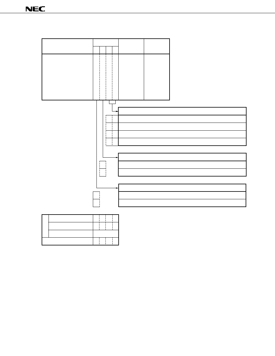
181
�
PD17704, 17705, 17707, 17708, 17709
Figure 13-22. Configuration of Timer 2 Counter Clock Selection Register
Caution
When the TM2RES flag is read, 0 is always read.
Name
Flag symbol
b
3
T
M
2
E
N
b
2
T
M
2
R
E
S
b
1
T
M
2
C
K
1
b
0
T
M
2
C
K
0
Address
29H
Read/Write
R/W
Timer 2 counter clock selection
Power-ON reset
WDT&SP reset
CE reset
Clock stop
At reset
0
1
0
1
0
0
0
100 kHz (10 s)
10 kHz (100 s)
2 kHz (500 s)
1 kHz (1 ms)
Sets basic clock of timer 2 counter
0
0
0
0
0
0
0
0
1
1
Does not change
Resets counter
Resets timer 2 counter (valid on writing)
0
1
0
0
0
Retained
Stops
Starts
Starts or stops timer 2
0
1
�
�
�
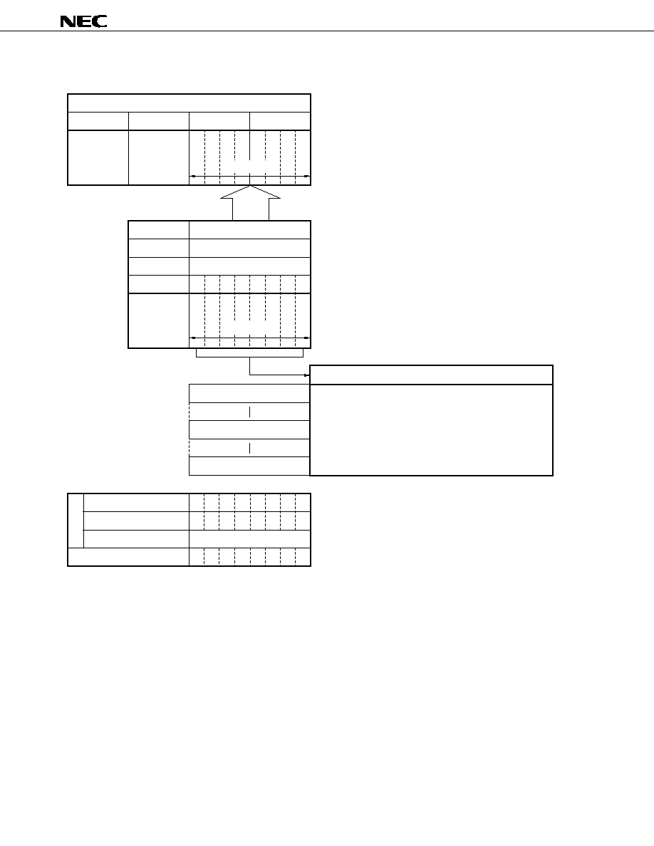
�
PD17704, 17705, 17707, 17708, 17709
182
Figure 13-23. Configuration of Timer 2 Counter
Reads count value of timer 2
Data buffer
DBF3
Don't care
DBF2
Don't care
Name
Symbol
Address
Bit
Data
DBF1
DBF0
b
3
b
2
b
1
b
0
b
7
b
6
b
5
b
4
Timer 2 counter
TM2C
1FH
Power-ON reset
WDT&SP reset
CE reset
Clock stop
At reset
0
0
0
0
0
0
0
0
0
0
0
0
0
0
0
0
0
0
0
0
0
0
0
0
Retained
Transfer data
Valid data
0
x
Count value
0FFH
8 bits
GET
PUT must not be executed

183
�
PD17704, 17705, 17707, 17708, 17709
Figure 13-24. Configuration of Timer 2 Modulo Register
Sets modulo data of timer 2
Data buffer
DBF3
Don't care
DBF2
Don't care
Name
Symbol
Address
Bit
Data
DBF1
DBF0
b
3
b
2
b
1
b
0
b
7
b
6
b
5
b
4
Timer 2 modulo register
TM2M
1EH
Power-On reset
WDT&SP reset
CE reset
Clock stop
At reset
1
1
1
1
1
1
1
1
1
1
1
1
1
1
1
1
1
1
1
1
1
1
1
1
Retained
Transfer data
Valid data
0
1
x
Setting prohibited
Modulo counter value
0FFH
8 bits
GET
PUT

�
PD17704, 17705, 17707, 17708, 17709
184
13.5.4 Example of using timer 2
(1) Modulo timer
The modulo timer is used for time management by generating a timer 2 interrupt at fixed intervals.
An example of a program is shown below.
This program executes processing B every 500
�
s.
TM2DATA
DAT
0032H
; Count data = 50
START:
BR
INITIAL
; Reset address
; Interrupt vector address
NOP
; SIO1
NOP
; SIO0
NOP
; TM3
BR
INT_TM2
; TM2
NOP
; TM1
NOP
; TM0
NOP
; INT4
NOP
; INT3
NOP
; INT2
NOP
; INT1
NOP
; INT0
NOP
; Down edge of CE
INITIAL:
INITFLG
NOT TM2EN, TM2RES, NOT TM2CK1, NOT TM2CK0
;
(Stop) , (Reset) , (Basic clock = 10
�
s)
MOV
DBF0, #TM2DATA
MOV
DBF1, #TM2DATA SHR4 AND 0FH
PUT
TM2, DBF
SET1
TM2EN
; START
SET1
IPTM2
; Enables timer 2 interrupt
EI
LOOP:
Processing A
BR
LOOP
INT_TM2:
PUT
DBFSTK, DBF
; Saves data buffer
INITFLG
TM2EN, TM2RES
; Resets and starts
Processing B
GET
DBF, DBFSTK
EI
RETI
; Return
END

185
�
PD17704, 17705, 17707, 17708, 17709
13.5.5 Error of timer 2
Timer 2 has an error of up to 1 basic clock in the following cases.
(1) On starting/stopping counter
The counter is started or stopped by setting the TM2EN flag.
Therefore, an error of 0 to +1 clocks occurs when the TM2EN flag is set, and an error of �1 to 0 clocks
occurs when the flag is reset.
In all, an error of
�
1 count occurs.
(2) On resetting counter operation
An error of 0 to +1 clocks occurs when the counter is reset.
(3) On selecting basic clock during counter operation
An error of 0 to +1 clocks of the newly selected clock occurs.
13.5.6 Cautions on using timer 2
Timer 2 interrupt may occur simultaneously with the other timer interrupts and CE reset. If it is necessary
to update the timer at CE reset, do not use timer 2, use basic timer 0 instead.
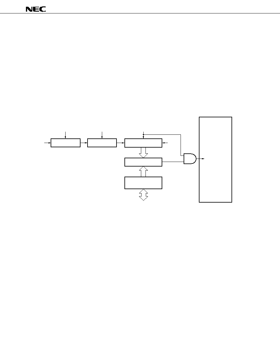
�
PD17704, 17705, 17707, 17708, 17709
186
13.6 Timer 3
13.6.1 Outline of timer 3
Figure 13-25 outlines timer 3.
Timer 3 counts the basic clock (1.125 MHz or 112.5 kHz selectable) with an 8-bit counter
Note
, and compares
the count value with a value set in advance.
Because timer 3 is multiplexed with a D/A converter, all the three D/A converter pins are automatically set
in the general-purpose port mode when timer 3 is used.
Note
A 9-bit or 8-bit counter can be selected for the D/A converter, but the 8-bit counter is automatically
selected when the timer function is selected.
Figure 13-25. Outline of Timer 3
Remarks 1. PWMCK (bit 0 of PWM clock selection register: refer to Figure 13-26) selects the output
frequency of timer 3.
2. TM3SEL (bit 3 of timer 3 control register: refer to Figure 13-27) selects timer 3 or D/A converter.
3. TM3EN (bit 1 of timer 3 control register: refer to Figure 13-27) starts or stops counting by timer
3.
4. TM3RES (bit 0 of timer 3 control register: refer to Figure 13-27) controls resetting of timer 3
counter.
Clock selection
4.5 MHz
Start/stop
Timer 3 counter (TM3C)
PWMCK flag
TM3EN flag
TM3SEL flag
Coincidence detection circuit
TM3RES
flag
DBF
IRQTM3 flag
Interrupt control
Timer 3 modulo register
(TM3M)

187
�
PD17704, 17705, 17707, 17708, 17709
13.6.2 Clock selection block
The clock of timer 3 is selected by the PWMCK flag of the PWM clock selection register.
Figure 13-26 shows the configuration of the flag.
Figure 13-26. Configuration of PWM Clock Selection Register
Name
Flag symbol
b
3
0
b
2
P
W
M
B
I
T
b
1
0
b
0
P
W
M
C
K
Address
26H
Read/Write
R/W
PWM clock selection
Power-ON reset
WDT&SP reset
CE reset
Clock stop
R:Retained
At reset
0
1
0
0
R
0
4.4 kHz (8 bits)/2.2 kHz (9 bits)
440 Hz (8 bits)/220 Hz (9 bits)
Selects output frequency of timer 3
0
0
0
R
0
Fixed to "0"
Fixed to "0"
8 bits
9 bits
0
Selects number of bits of PWM counter
0
1

�
PD17704, 17705, 17707, 17708, 17709
188
13.6.3 Start/stop control block
The start/stop block starts or stops the basic clock to be input to timer 3 counter by using the TM3EN flag.
To control timer 3, timer 3 must be selected by the TM3SEL flag.
Figure 13-27 shows the configuration of each flag.
Figure 13-27. Configuration of Timer 3 Control Register
Name
Flag symbol
b
3
T
M
3
S
E
L
b
2
0
b
1
T
M
3
E
N
b
0
T
M
3
R
E
S
Address
28H
Read/Write
R/W
Timer 3 control
0
1
Dose not change
Resets
Resets counter
Stop
Starts
Fixed to "0"
Starts or stops counter
0
1
D/A converter (PWM output)
Timer 3
Selects timer 3 or D/A converter
0
1
Power-ON reset
WDT&SP reset
CE reset
Clock stop
R:Retained
At reset
0
0
0
0
0
0
R
0
0
0
0
Retained

189
�
PD17704, 17705, 17707, 17708, 17709
13.6.4 Count block
The count block counts the basic clock with timer 3 and issues an interrupt request when the count value of
timer 3 coincides with the value of the timer 3 modulo register.
Timer 3 counter can be reset by the TM3RES flag.
Because the PWM data register 2 (PWMR2) and timer 3 modulo register (TM3M) are multiplexed, these
registers cannot be used at the same time.
When timer 3 is used, the PWM data register 1 (PWMR1) and PWM data register 0 (PWMR0) can be used
as 9-bit data latches (refer to 15. D/A CONVERTER (PWM mode)).
Figure 13-28. Configuration of Timer 3 Modulo Register
Note
This register is multiplexed with the PWM data register.
Sets modulo data of timer 3
Data buffer
DBF3
DBF2
Name
Symbol
Address
Bit
Data
DBF1
DBF0
b
3
b
2
b
1
b
0
b
7
b
8
b
9
0
b
10
0
b
11
0
b
12
0
b
13
0
b
14
0
b
15
0
b
6
b
5
b
4
Timer 3 modulo register
Note
TM3M
46H
Power-ON reset
WDT&SP reset
CE reset
Clock stop
At reset
1
1
1
1
1
1
1
1
1
1
1
1
1
1
1
1
1
1
1
1
1
1
1
1
1
1
1
Retained
Transfer data
Valid data
0
x
Modulo counter value
Fixed to "0"
1FFH
16 bits
GET
PUT

�
PD17704, 17705, 17707, 17708, 17709
190
13.6.5 Example of using timer 3
An example of a program using timer 3 (multiplexed with PWM) is given below.
This program executes processing B every 888
�
s.
TM3DATA
DAT
0064H
; Count data = 100
START:
BR
INITIAL
; Reset address
; Interrupt vector address
NOP
; SIO1
NOP
; SIO0
BR
INT_TM3
; TM3
NOP
; TM2
NOP
; TM1
NOP
; TM0
NOP
; INT4
NOP
; INT3
NOP
; INT2
NOP
; INT1
NOP
; INT0
NOP
; Down edge of CE
INITIAL:
INITFLG
NOT PWMSEL2 , NOT PWMSEL1 , NOT PWMSEL0
;
(General-purpose port), (General-purpose port), (General-purpose port)
INITFLG
NOT PWMBIT, PWMCK
;
( 8BIT ), (440 Hz)
INITFLG
TM3SEL , NOT TM3EN, TM3RES
;
(Timer 3 mode), (Stop) , (Reset)
MOV
DBF0, #TM3DATA
MOV
DBF1, #TM3DATA SHR4 AND 0FH
PUT
TM3M, DBF
SET1
TM3EN
; START
SET1
IPTM3
; Enables timer 3 interrupt
EI
LOOP:
Processing A
BR
LOOP
INT_TM3:
PUT
DBFSTK, DBF
; Saves data buffer
Processing B
GET
DBF, DBFSTK
EI
RETI
; Return
END

191
�
PD17704, 17705, 17707, 17708, 17709
13.6.6 Error of timer 3
Timer 3 has an error of up to 1 basic clock in the following cases.
(1) On starting/stopping counter
The counter is started or stopped by setting the TM3EN flag.
Therefore, an error of 0 to +1 clocks occurs when the TM3EN flag is set, and an error of �1 to 0 clocks
occurs when the flag is reset.
In all, an error of
�
1 count occurs.
(2) On resetting counter operation
An error of 0 to +1 clocks occurs when the counter is reset.
(3) On selecting basic clock during counter operation
An error of 0 to +1 clocks of the newly selected clock occurs.
13.6.7 Cautions on using timer 3
Timer 3 interrupt may occur simultaneously with the other timer interrupts and CE reset. If it is necessary
to update the timer at CE reset, do not use timer 3, use basic timer 0 instead.
When timer 3 is used, the three output port pins multiplexed with the D/A converter pins, P1B2/PWM2 through
P1B0/PWM0, are automatically set in the general-purpose output port mode.

�
PD17704, 17705, 17707, 17708, 17709
192
13.6.8 Status at reset
(1) At power-ON reset
The P1B2/PWM2 through P1B0/PWM0 pins are set in the general-purpose output port mode.
The output value is "low level".
The value of each PWM data register (including the timer 3 modulo register) is "1FFH".
(2) At WDT&SP reset
The P1B2/PWM2 through P1B0/PWM0 pins are set in the general-purpose output port mode.
The output value is "low level".
The value of each PWM data register (including the timer 3 modulo register) is "1FFH".
(3) On execution of clock stop instruction
The P1B2/PWM2 through P1B0/PWM0 pins are set in the general-purpose output port mode.
The output value is the "previous contents of the output latch".
The value of each PWM data register (including the timer 3 modulo register) is "1FFH".
(4) At CE reset
The previous status is retained.
That is, if the D/A converter is being used, the PWM output is retained as is. If timer 3 is being used,
counting continues.
While timer 3 is being used, the DI status is set (in which all interrupts are disabled).
(5) In halt status
The previous status is retained.
That is, if the D/A converter is being used, the PWM output is retained as is. If timer 3 is being used,
counting continues.
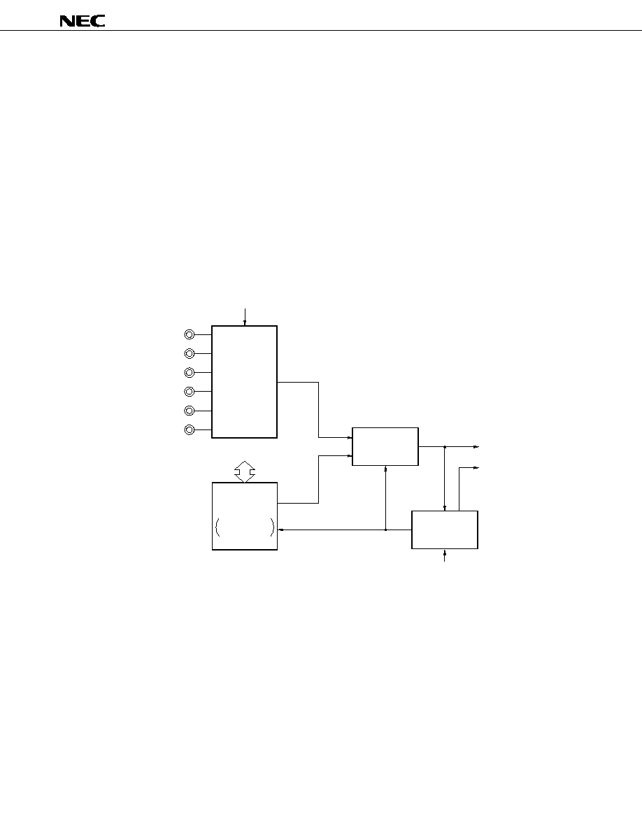
193
�
PD17704, 17705, 17707, 17708, 17709
14. A/D CONVERTER
14.1 Outline of A/D Converter
Figure 14-1 outlines the A/D converter.
The A/D converter converts an analog voltage input to the AD5 to AD0 pins into an 8-bit digital signal.
Two modes can be selected by using the ADCMD flag: software mode and hardware mode.
In the software mode, a voltage input to a pin is compared with an internal reference voltage, and the result
of the comparison is detected by the ADCCMP flag. By judging this result in software and by sequentially
selecting reference voltages, the A/D converter can be used as a successive approximation A/D converter.
In the hardware mode, reference voltages are automatically selected, and the input voltage is directly
detected as 8-bit digital data.
Figure 14-1. Outline of A/D Converter
Remarks 1. ADCCH2 through ADCCH0 (bits 2 through 0 of A/D converter channel selection register: refer
to Figure 14-3) select pins used for the A/D converter.
2. ADCCMP (bit 0 of A/D converter mode selection register: refer to Figure 14-5) detects the
result of comparison.
3. ADCSTT (bit 1 of A/D converter mode selection register: refer to Figure 14-5) detects the
operating status.
4. ADCMD (bit 2 of A/D converter mode selection register: refer to Figure 14-5) selects software
or hardware mode.
P1C3/AD5
P1C2/AD4
P0D3/AD3
P0D2/AD2
P0D1/AD1
P0D0/AD0
ADCCH2 flag
ADCCH1 flag
ADCCH0 flag
Input selection
block
Compare voltage
generation block
R-string
D/A converter
DBF
ADCMD flag
ADCCMP flag
ADCSTT flag
Start/stop control
block
Compare block
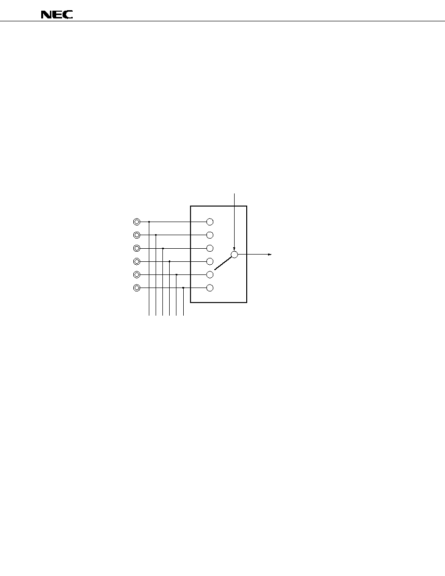
�
PD17704, 17705, 17707, 17708, 17709
194
14.2 Input Selection Block
Figure 14-2 shows the configuration of the input selection block.
The input selection block selects a pin to be used by using the ADCCH2 through ADCCH0 flags. Only one
pin can be used for the A/D converter. When one of the P0D0/AD0 through P0D3/AD3, P1C2/AD4, and P1C3/
AD5 pins is selected, the other five pins are forcibly set in the input port mode.
The P0D0/AD0 through P0D3/AD3 pins can be connected to a pull-down resistor if so specified by the P0DPL0
through P0DPLD3 flags. To use the P0D0/AD0 through P0D3/AD3 pins for the A/D converter, therefore,
disconnect their pull-down resistors to correctly detect an external input analog voltage.
Figure 14-3 shows the configuration of the A/D converter channel selection register.
Figure 14-2. Configuration of Input Selection Block
P1C3/AD5
P1C2/AD4
P0D3/AD3
P0D2/AD2
P0D1/AD1
P0D0/AD0
Selector
Each I/O port
ADCCH2
ADCCH1
ADCCH0
Compare block
V
ADCIN

195
�
PD17704, 17705, 17707, 17708, 17709
Figure 14-3. Configuration of A/D Converter Channel Selection Register
Name
Flag symbol
b
3
0
b
2
A
D
C
C
H
2
b
1
A
D
C
C
H
1
b
0
A
D
C
C
H
0
Address
24H
Read/Write
R/W
A/D converter channel selection
Power-ON reset
WDT&SP reset
CE reset
Clock stop
At reset
0
1
0
1
0
1
0
1
0
0
A/D converter not used (general-purpose input port)
P0D0/AD0 pin
P0D1/AD1 pin
P0D2/AD2 pin
P0D3/AD3 pin
P1C2/AD4 pin
P1C3/AD5 pin
Setting prohibited
Fixed to "0"
Selects pin used for A/D converter
0
0
0
0
0
1
1
0
0
1
1
0
0
0
0
1
1
1
1
0
0
Retained
Retained
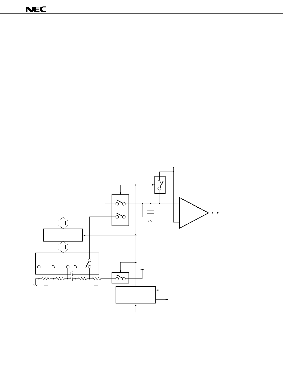
�
PD17704, 17705, 17707, 17708, 17709
196
14.3 Compare Voltage Generation and Compare Blocks
Figure 14-4 shows the configuration of the compare voltage generation block and compare block.
The compare voltage generation block switches a tap decoder according to the 8-bit data set to the A/D
converter reference voltage setting register and generates 256 different of compare voltages V
ADCREF
.
In other words, this block is an R-string D/A converter.
The supply voltage to this R-string D/A converter is the same as the supply voltage V
DD
of the device.
The compare block compares voltage V
ADCIN
input from a pin with compare voltage V
ADCREF
.
Comparison can be made in two modes, software mode and hardware mode, which can be selected by the
ADCMD flag.
In the software mode, a compare voltage is set to the A/D converter reference voltage setting register by
software, and one set compare voltage is compared with the input voltage, and the result of the comparison is
detected by the ADCCMP flag.
In the hardware mode, once comparison has been started, the hardware automatically changes the value of
the A/D converter reference voltage setting register. On completion of the comparison, the value of the A/D
converter reference voltage setting register is read and is loaded as an 8-bit data.
Figures 14-5 and 14-6 show the configuration of each flag and A/D converter reference voltage setting
register.
Figure 14-4. Configuration of Compare Voltage Generation and Compare Blocks
DBF
Tap decoder
0
1
2
254
255
V
DD
A/D converter reference
voltage setting register (ADCR)
1
2
R
R
R
3
2
R
Soft/hard,
start/stop
control block
ADCMD flag
ADCSTT flag
ADCCMP
flag
Comparator
-
+
2 pF
1/2 V
DD
V
ADCIN
V
ADCREF

197
�
PD17704, 17705, 17707, 17708, 17709
Figure 14-5. Configuration of A/D Converter Mode Selection Register
Notes 1. A/D conversion under execution is stopped if "0" is written to this bit.
2. A/D operation is started in the hardware mode when "1" is written to this bit. In the software mode,
operation is started as soon as data has been written (by the PUT instruction) to the A/D converter
reference voltage setting register (ADCR).
Name
Flag symbol
b
3
0
b
2
A
D
C
M
D
b
1
A
D
C
S
T
T
b
0
A
D
C
C
M
P
Address
25H
Read/Write
R/W
A/D converter mode selection
Power-ON reser
WDT&SP reser
CE reser
Clock stop
R:Retained
At reset
0
1
0
0
0
R
V
ADCIN
< V
ADCREF
V
ADCIN
> V
ADCREF
Detects result of comparison by A/D converter
0
0
0
R
R
End of conversion
Conversion in progress
Software mode
Note 1
Hardware mode
Note 2
Detects operating status of A/D converter in hardware mode
0
1
0
0
0
0
Selects compare mode of A/D converter and starts or stops A/D converter
0
1
Fixed to "0"

�
PD17704, 17705, 17707, 17708, 17709
198
Figure 14-6. Configuration of A/D Converter Reference Voltage Setting Register
Note
"0" in the hardware mode.
Sets or reads compare voltage V
ADCREF
of A/D converter
� In software mode: Sets compare voltage
� In hardware mode: Reads result of comparison
Data buffer
DBF3
Don't care
DBF2
Don't care
Name
Symbol
Address
Bit
Data
DBF1
DBF0
b
3
b
2
b
1
b
0
b
7
b
6
b
5
b
4
A/D converter reference volfage setting register
ADCR
02H
Power-ON reset
WDT&SP reset
CE reset
Clock stop
At reset
0
0
Retained
Note
Retained
Note
Transfer data
Valid data
0
x
x-0.5
256
V
ADCREF
= 0 V
V
ADCREF
=
�
V
DD
(V)
FFH
8 bits
GET
PUT
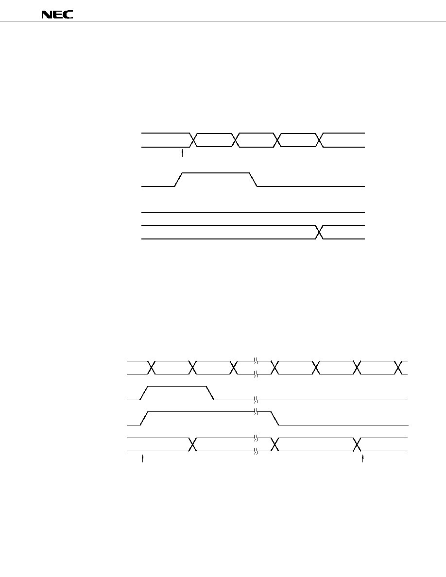
199
�
PD17704, 17705, 17707, 17708, 17709
14.4 Comparison Timing Chart
14.4.1 In software mode
Comparison is completed three instructions after data has been set (by the PUT instruction) to the A/D
converter reference voltage setting register (ADCR).
Figure 14-7 shows the timing chart.
Figure 14-7. Timing Chart of Comparison by A/D Converter
14.4.2 In hardware mode
When the ADCMD flag is set to "1", A/D conversion is started. The ADCSTT flag is set to "1", and comparison
is completed after 17 instructions have been executed. At this time, the ADCSTT flag is reset to "0" after 15
instructions have been executed after the ADCMD flag was set to "1". This is because execution time of two
instructions is required to judge the status of the ADCSTT flag. For details, also refer to 14.5 Using A/D
Converter.
Figure 14-8 shows the timing chart.
Figure 14-8. Timing Chart of Comparison by A/D Converter
Instruction cycle
1
"0"
PUT ADCR, DBF
2
Result of comparison
3
Sample & hold
ADCSTT fiag
ADCCMP fiag
Comparison starts
Instruction cycle
1
2
1st
8th
Result of comparison
3
15
16
17
Sample & hold
ADCSTT flag
Reference voltage setting register
A/D converter
ADCMD flag (=1) set.
Comparison starts
End of comparison

�
PD17704, 17705, 17707, 17708, 17709
200
14.5 Using A/D Converter
14.5.1 Software mode
The software mode is convenient for comparing one compare voltage.
An example of a program in this mode is shown below.
Example To compare input voltage V
ADCIN
of AD0 pin with compare voltage V
ADCREF
(127.5/256 V
DD
), and
branch to AAA if V
ADCIN
< V
ADCREF
, or to BBB if V
ADCIN
> V
ADCREF
ADCR7 FLG
0.0EH.3 ; Defines each bit of DBF as ADCR data setting flag
ADCR6 FLG
0.0EH.2
ADCR5 FLG
0.0EH.1
ADCR4 FLG
0.0EH.0
ADCR3 FLG
0.0EH.3
ADCR2 FLG
0.0EH.2
ADCR1 FLG
0.0EH.1
ADCR0 FLG
0.0EH.0
BANK15
INITFLG NOT P0DPLD3, NOT P0DPLD2, NOT P0DPLD1, P0DPLD0
; Disconnects pull-down resistor of P0D0 pin
BANK0
INITFLG NOT ADCCH2, NOT ADCCH1, ADCCH0
; Selects AD0 pin for A/D converter
CLR1
ADCMD
; Sets software mode
INITFLG ADCR7, NOT ADCR6, NOT ADCR5, NOT ADCR4
;
INITFLG NOT ADCR3, NOT ADCR2, NOT ADCR1, NOT ADCR0
;
PUT
ADCR, DBF
; Sets compare voltage V
ADCREF
NOP
; Waits for duration of three instructions
NOP
;
NOP
;
SKT1
ADCCMP
; Judges result of comparison
BR
AAA
BR
BBB
14.5.2 Hardware mode
Here is a program example:
Example To detect the value of analog input roltage V
ADCIN
of AD0 pin.
BANK15
INITFLG NOT P0DPLD3, NOT P0DPLD2, NOT P0DPLD1, P0DPLD0 ; Disconnects pull-down resistor of P0D0 pin
BANK0
INITFLG NOT ADCCH2, NOT ADCCH1, ADCCH0
; Selects AD0 pin for A/D converter
SET1
ADCMD
; Sets hardware mode and starts conversion
LOOP:
SKT1
ADCSTT
; Detects end of A/D conversion
; Embedded macro instruction
;PEEK WR, .MF. ADCSTT SHR4 AND 0FH
;SKT1 WR,#.DF.ADCSTT AND 0FH
BR
LOOP
; Conversion in progress
GET
DBF,ADCR
; Stores result of conversion to DBF

201
�
PD17704, 17705, 17707, 17708, 17709
14.6 Cautions on Using A/D Converter
14.6.1 Cautions on selecting A/D converter pin
When one of the P0D0/AD0 through P0D3/AD3, P1C2/AD4, and P1C3/AD5 pins is selected, the other five
pins are forcibly set in the input port mode. The P0D0/AD0 through P0D3/AD3 pins can be connected to a pull-
down resistor if so specified by the P0DPL0 through P0DPLD3 flags in bank 15. To use the P0D0/AD0 through
P0D3/AD3 pins for the A/D converter, therefore, disconnect their pull-down resistors to correctly detect an
external input analog voltage.
14.7 Status at Reset
14.7.1 At power-ON reset
All the P0D0/AD0 through P0D3/AD3, P1C2/AD4, and P1C3/AD5 pins are set in the general-purpose input
port mode.
The P0D0 through P0D3 pins are connected with a pull-down resistor.
14.7.2 At WDT&SP reset
All the P0D0/AD0 through P0D3/AD3, P1C2/AD4, and P1C3/AD5 pins are set in the general-purpose input
port mode.
The P0D0 through P0D3 pins are connected with a pull-down resistor.
14.7.3 At CE reset
The status of the pin selected for the A/D converter is retained as is.
The previous status of the pull-down resistor of the P0D0 through P0D3 pins is retained.
14.7.4 On execution of clock stop instruction
The status of the pin selected for the A/D converter is retained as is.
The previous status of the pull-down resistor of the P0D0 through P0D3 pins is retained.
14.7.5 In halt status
The status of the pin selected for the A/D converter is retained as is.
The previous status of the pull-down resistor of the P0D0 through P0D3 pins is retained.
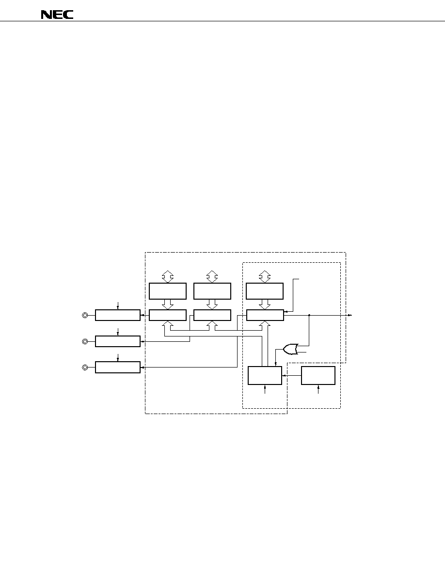
202
�
PD17704, 17705, 17707, 17708, 17709
15. D/A CONVERTER (PWM mode)
15.1 Outline of D/A Converter
Figure 15-1 outlines the D/A converter.
The D/A converter outputs a signal whose duty factor is varied by means of PWM (Pulse Width Modulation). By
connecting an external lowpass filter to the D/A converter, a digital signal can be converted into an analog signal.
Each pin of the D/A converter can output a variable-duty signal independently of the others.
Whether an 8-bit counter or 9-bit counter is used for the D/A converter can be specified by software.
When the 8-bit counter is selected, two output frequencies, 4.4 kHz and 440 Hz can be selected, and the duty factor
of the output signal can be varied in 256 steps.
When the 9-bit counter is selected, two output frequencies, 2.2 kHz and 220 Hz, can be selected, and the duty
factor can be varied in 512 steps.
When the D/A converter is not used, it can be used as timer 3, which counts the basic clock (1.125 or 0.1125 MHz)
with an 8-bit counter.
For the details of timer 3, refer to 13. TIMER 3.
Figure 15-1. Outline of D/A Converter
Remarks 1.
PWM2SEL through PWM0SEL (bits 2 through 0 of PWM/general-purpose port pin function selection
register: refer to Figure 15-4) select a general-purpose output port of D/A converter.
2.
PWMBIT (bit 2 of PWM clock selection register: refer to Figure 15-2) selects the number of bits (8
or 9 bits) of the PWM counter.
3.
PWMCK (bit 0 of PWM clock selection register: refer to Figure 15-2) selects the output frequency
of PWM timer.
4.
TM3SEL (bit 3 of timer 3 control register: refer to Figure 15-5) selects timer 3 or D/A converter.
5.
TM3RES (bit 0 of timer 3 control register: refer to Figure 15-5) controls resetting of timer 3 counter.
P1B0/PWM0
P1B1/PWM1
P1B2/PWM2
PWM0SEL flag
DBF
DBF
DBF
Multiplexed with timer 3
Duty setting block
TM3SEL flag
TM3RES flag
RES
f
PWM
IRQTM3
Comparator
Comparator
Comparator
PWMBIT
PWMCK
Clock generation
block
9-bit or
8-bit counter
PWM data register 0
(PWMR0)
PWM data register 1
(PWMR1)
PWM data register 2
(PWMR2)
Output selection block
Output selection block
Output selection block
PWM1SEL flag
PWM2SEL flag

203
�
PD17704, 17705, 17707, 17708, 17709
15.2 PWM Clock Selection Register
The PWM clock selection register specifies whether the PWM counter is used as an 8-bit counter or 9-bit counter
when the D/A converter is used for PWM output.
Figure 15-2 shows the configuration of the PWM clock selection register.
Figure 15-2. Configuration of PWM Clock Selection Register
Name
Flag symbol
b
3
0
b
2
P
W
M
B
I
T
b
1
0
b
0
P
W
M
C
K
Address
26H
Read/Write
R/W
PWM clock selection
Power-ON reset
WDT&SP reset
CE reset
Clock stop
R: Retained
At reset
0
1
0
0
R
0
4.4 kHz (8 bits) /2.2 kHz (9 bits)
440 Hz (8 bits) /220 Hz (9 bits)
Selects output frequency of timer 3
0
0
0
R
0
Fixed to
"
0
"
Fixed to
"
0
"
8 bits
9 bits
0
Selects number of bits of PWM counter
0
1
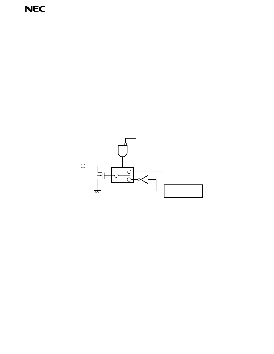
204
�
PD17704, 17705, 17707, 17708, 17709
15.3 PWM Output Selection Block
The output selection block specifies whether each output pin of the D/A converter is used for the D/A converter
or as a general-purpose output port, by using the PWM2SEL through PWM0SEL flags of the PWM/general-purpose
port pin function selection register.
Figure 15-3 shows the configuration of the output selection block, and Figure 15-4 shows the configuration of the
PWM/general-purpose port pin function selection register.
Each pin can be changed between the D/A converter mode and general-purpose output port mode independently
of the others.
Because each output pin is an N-ch open-drain output pin, an external pull-up resistor is necessary.
When the D/A converter is used as timer 3, the P1B2/PWM2 through P1B0/PWM0 pins are automatically set in
the general-purpose output port mode, regardless of the values set to the PWM2SEL through PWM0SEL flags.
Figure 15-3. Configuration of Output Selection Block
PWM2SEL through PWM0SEL flags
TM3SEL
Comparator output
Output latch
1
0
Each output pin
205
�
PD17704, 17705, 17707, 17708, 17709
Figure 15-4. Configuration of PWM/General-Purpose Port Pin Function Selection Register
Name
Flag symbol
b
3
0
b
2
P
W
M
2
S
E
L
b
1
P
W
M
1
S
E
L
b
0
P
W
M
0
S
E
L
Address
27H
Read/Write
R/W
PWM/general-purpose port
pin function selection
Power-ON reset
WDT&SP reset
CE reset
Clock stop
Retained
At reset
0
1
0
0
0
General-purpose output port
D/A converter
Selects function of P1B0/PWM0 pin
0
0
0
0
General-purpose output port
D/A converter
General-purpose output port
D/A converter
Selects function of P1B1/PWM1 pin
0
1
0
0
0
Selects function of P1B2/PWM2 pin
0
1
Fixed to
"
0
"
206
�
PD17704, 17705, 17707, 17708, 17709
Figure 15-5. Configuration of Timer 3 Control Register
Name
Flag symbol
b
3
T
M
3
S
E
L
b
2
0
b
1
T
M
3
E
N
b
0
T
M
3
R
E
S
Address
28H
Read/Write
R/W
Timer 3 control
0
1
Does not change
Resets
Resets counter
Stops
Starts
Fixed to
"
0
"
Starts or stops counter
0
1
D/A converter (PWM output)
Timer 3
Selects timer 3 or D/A converter
0
1
Power-ON reset
WDT&SP reset
CE reset
Clock stop
R: Retained
At reset
0
0
0
0
0
0
R
0
0
0
0
Retained

207
�
PD17704, 17705, 17707, 17708, 17709
15.4 Duty Setting Block
15.4.1 PWM duty with 8-bit counter selected
The duty setting block compares the value set to each PWM data register (PWMR2 to PWMR0) with the value of
the basic clock counted by each 8-bit counter. If the value of the PWM data register is greater, the block outputs a
high level. If the value of the PWM data register is less, it outputs a low level.
Where the value set to the PWM data register is "x", therefore, the duty factor can be calculated by the following
expression.
Duty: D =
x + 0.25
�
100%
256
Remark
0.25 is an offset, and a high level is output even where x = 0.
Data is set to each PWM data register for each pin via data buffer (DBF). However, the same basic clock, PWM
counter, and output frequency must be selected for each pin. This means that each pin cannot output a duty factor
of a different cycle independently of the others.
Because the basic clock frequency is 1.125 or 0.1125 MHz, the frequency and cycle of the output signal can be
calculated as follows.
(1) Where output frequency is 4.4 kHz and basic clock frequency is 1.125 MHz
Frequency: f =
1.125 MHz
= 4.3945 kHz
256
Cycle:
T =
256
= 227.56
�
s
1.125 MHz
(2) Where output frequency is 440 Hz and basic clock frequency is 0.1125 MHz
Frequency: f =
0.1125 MHz
= 439.45 Hz
256
Cycle:
T =
256
= 2.2756 ms
0.1125 MHz
Because the duty setting register of the PWM data registers and timer 3 modulo register are the same register,
they cannot be used at the same time.
When timer 3 is used, PWM data registers 1 and 0 can be used as 8-bit data latches.

208
�
PD17704, 17705, 17707, 17708, 17709
Figure 15-6. Configuration of PWM Data Registers (with 8-bit counter selected)
Note
This register is multiplexed with timer 3 modulo register.
Sets PWM output duty of each pin
Data buffer
DBF3
DBF2
Name
Symbol
Address
Bit
Data
DBF1
DBF0
b
3
b
2
b
1
b
0
b
7
b
8
0
b
9
0
b
10
0
b
11
0
b
12
0
b
13
0
b
14
0
b
15
0
b
6
b
5
b
4
PWM data register 2
Note
PWMR2
46H
Power-ON reset
WDT&SP reset
CE reset
Clock stop
At reset
1
1
1
1
1
1
1
1
1
1
1
1
1
1
1
1
1
1
1
1
1
1
1
1
Retained
Transfer data
Valid data
0
x
Duty: D =
Fixed to
"
0
"
FFH
16 bits
GET
PUT
Name
Symbol
Address
Bit
Data
b
3
b
2
b
1
b
0
b
7
b
8
0
b
9
0
b
10
0
b
11
0
b
12
0
b
13
0
b
14
0
b
15
0
b
6
b
5
b
4
PWM data register 1
PWMR1
45H
Valid data
GET
PUT
Name
Symbol
Address
Bit
Data
b
3
b
2
b
1
b
0
b
7
b
8
0
b
9
0
b
10
0
b
11
0
b
12
0
b
13
0
b
14
0
b
15
0
b
6
b
5
b
4
PWM data register 0
PWMR0
44H
Valid data
GET
PUT
x+0.25
256
�
100 %

209
�
PD17704, 17705, 17707, 17708, 17709
15.4.2 PWM duty with 9-bit counter selected
The duty setting block compares the value set to each PWM data register (PWMR2 to PWMR0) with the value of
the basic clock counted by each 9-bit counter. If the value of the PWM data register is greater, the block outputs a
high level. If the value of the PWM data register is less, it outputs a low level.
Where the value set to the PWM data register is "x", therefore, the duty factor can be calculated by the following
expression.
Duty: D =
x + 0.25
�
100%
512
Remark
0.25 is an offset, and a high level is output even where x = 0.
Data is set to each PWM data register for each pin via data buffer (DBF). However, the same basic clock, PWM
counter, and output frequency must be selected for each pin. This means that each pin cannot output a duty factor
of a different cycle independently of the others.
Because the basic clock frequency is 1.125 or 0.1125 MHz, the frequency and cycle of the output signal can be
calculated as follows.
(1) Where output frequency is 2.2 kHz and basic clock frequency is 1.125 MHz
Frequency: f =
1.125 MHz
= 2.197 kHz
512
Cycle:
T =
512
= 455.11
�
s
1.125 MHz
(2) Where output frequency is 220 Hz and basic clock frequency is 0.1125 MHz
Frequency: f =
0.1125 MHz
= 219.73 Hz
512
Cycle:
T =
512
= 4.5511 ms
0.1125 MHz
Because the duty setting register of the PWM data registers and timer 3 modulo register are the same register,
they cannot be used at the same time.
When timer 3 is used, PWM data registers 1 and 0 can be used as 8-bit data latches.

210
�
PD17704, 17705, 17707, 17708, 17709
Figure 15-7. Configuration of PWM Data Registers (with 9-bit counter selected)
Note
This register is multiplexed with timer 3 modulo register.
Sets PWM output duty of each pin
Data buffer
DBF3
DBF2
Name
Symbol
Address
Bit
Data
DBF1
DBF0
b
3
b
2
b
1
b
0
b
7
b
8
b
9
0
b
10
0
b
11
0
b
12
0
b
13
0
b
14
0
b
15
0
b
6
b
5
b
4
PWM data register 2
Note
PWMR2
46H
Power-On reset
WDT&SP reset
CE reset
Clock stop
At reset
1
1
1
1
1
1
1
1
1
1
1
1
1
1
1
1
1
1
1
1
1
1
1
1
1
1
1
Retained
Transfer data
Valid data
0
x
Duty: D =
Fixed to
"
0
"
1FFH
16 bits
GET
PUT
Name
Symbol
Address
Bit
Data
b
3
b
2
b
1
b
0
b
7
b
8
b
9
0
b
10
0
b
11
0
b
12
0
b
13
0
b
14
0
b
15
0
b
6
b
5
b
4
PWM data register 1
PWMR1
45H
Valid data
GET
PUT
Name
Symbol
Address
Bit
Data
b
3
b
2
b
1
b
0
b
7
b
8
b
9
0
b
10
0
b
11
0
b
12
0
b
13
0
b
14
0
b
15
0
b
6
b
5
b
4
PWM data register 0
PWMR0
44H
Valid data
GET
PUT
x+0.25
512
�
100 %

211
�
PD17704, 17705, 17707, 17708, 17709
15.5 Clock Generation Block
The clock generation block outputs a basic clock to set the duty factor of each output signal.
Two output frequencies, 1.125 MHz and 112.5 kHz, can be selected.
15.6 D/A Converter Output Wave
(1) shows the relationship between the duty factor and output wave.
(2) shows the output wave of each pin. Each output pin has a phase different from the others.
(1) Duty and output wave
(a) With 8-bit counter and 4.4 kHz selected
(b) With 8-bit counter and 440 Hz selected
222 ns
x = 0
x = 1
x = 2
x = 255
667 ns
888 ns
888 ns
227.56 s
.........
�
2.22 s
x = 0
x = 1
x = 2
x = 255
6.67 s
8.88 s
8.88 s
2.2756 ms
�
.........
�
�
�
212
�
PD17704, 17705, 17707, 17708, 17709
(c) With 9-bit counter and 2.2 kHz selected
(d) With 9-bit counter and 220 Hz selected
(2) Each pin and output wave
(a) With 8-bit counter and 4.4 kHz selected
222 ns
x = 0
x = 1
x = 2
x = 511
667 ns
888 ns
888 ns
455.11 s
.........
�
2.22 s
x = 0
x = 1
x = 2
x = 511
6.67 s
8.88 s 8.88 s
4.5511 ms
.........
�
�
�
�
222 ns
PWM0 (x = 0)
PWM1 (x = 0)
PWM2 (x = 0)
222 ns
222 ns
227.56 s
227.56 s
227.56 s
�
�
�
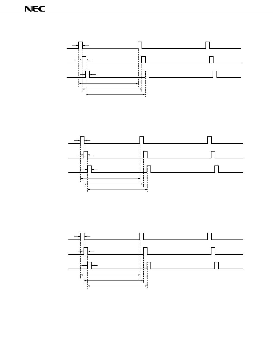
213
�
PD17704, 17705, 17707, 17708, 17709
(b) With 8-bit counter and 440 Hz selected
(c) With 9-bit counter and 2.2 kHz selected
(d) With 9-bit counter and 220 Hz selected
2.22 s
PWM0 (x = 0)
PWM1 (x = 0)
PWM2 (x = 0)
2.22 s
2.22 s
2.2756 ms
2.2756 ms
2.2756 ms
�
�
�
222 ns
PWM0 (x = 0)
PWM1 (x = 0)
PWM2 (x = 0)
222 ns
222 ns
455.11 s
455.11 s
455.11 s
�
�
�
2.22 s
PWM0 (x = 0)
PWM1 (x = 0)
PWM2 (x = 0)
2.22 s
2.22 s
4.5511 ms
4.5511 ms
4.5511 ms
�
�
�

214
�
PD17704, 17705, 17707, 17708, 17709
15.7 Example of Using D/A Converter
An example of a program using the D/A converter is shown below.
Example This program increments the duty factor of the PWM1 pin every 1 second.
PWM1DATA DAT 0000H
INITIAL:
INITFLG
NOT PWM2SEL, NOT PWM1SEL, NOT PWM0SEL
;
(General-purpose port), (General-purpose port), (General-purpose port)
INITFLG
PWMBIT , NOT PWMCK
;
(9-bit counter), (1.125 MHz)
LOOP0:
BANK1
CLR1
P1B1
BANK0
CLR1
TM3SEL
; Selects D/A converter
MOV
DBF2, #PWM1DATA SHR 8 AND 0FH
MOV
DBF1, #PWM1DATA SHR 4 AND 0FH
MOV
DBF0, #PWM1DATA AND 0FH
SET1
PWM1SEL
; Sets PWM1/P1B1 pin in PWM output port mode
LOOP1:
; Duty: 0.25/512 to 511.25/512 (PWM output)
PUT
PWM1R, DBF
GET2
TM3RES, TM3EN
; Resets and starts counter
Waits for 1 second
GET
DBF, PWM1R
ADD
DBF0, #1
ADDC
DBF1, #0
ADDC
DBF2, #1
SKGE
DBF2, #2
BR
LOOP1
LOOP2:
; Port outputs high level
BANK1
SET1
P1B1
BANK0
CLR1
PWM1SEL
; Sets PWM1/P1B1 pin in general-purpose output port mode
Waits for 1 second
BR
LOOP0

215
�
PD17704, 17705, 17707, 17708, 17709
15.8 Status at Reset
15.8.1 At power-ON reset
The P1B0/PWM0 through P1B2/PWM2 pins are set in the general-purpose output port mode.
The output value is "low level".
The value of each PWM data register (including the timer 3 modulo register) is "1FFH".
15.8.2 At WDT&SP reset
The P1B0/PWM0 through P1B2/PWM2 pins are set in the general-purpose output port mode.
The output value is "low level".
The value of each PWM data register (including the timer 3 modulo register) is "1FFH".
15.8.3 At CE reset
The P1B0/PWM2 through P1B2/PWM2 pins retain the previous status.
That is, if the D/A converter is being used, the PWM output is retained as is. If timer 3 is being used, counting
continues.
15.8.4 On execution of clock stop instruction
The P1B0/PWM0 through P1B2/PWM2 pins are set in the general-purpose output port mode.
The output value is the "previous contents of the output latch".
The value of each PWM data register (including the timer 3 modulo register) is "1FFH".
15.8.5 In halt status
The P1B0/PWM0 through P1B2/PWM2 pins retain the previous status.
That is, if the D/A converter is being used, the PWM output is retained as is. If timer 3 is being used, counting
continues.

216
�
PD17704, 17705, 17707, 17708, 17709
16. SERIAL INTERFACES
16.1 Outline of Serial Interfaces
Figure 16-1 outlines the serial interfaces.
Table 16-1 classifies the serial interfaces and shows their communication modes.
As shown in Figure 16-1, two serial interfaces, 0 (SIO0) and 1 (SIO1), are available.
Serial interfaces 0 and 1 can be used at the same time.
Serial interface 0 can be used in two modes: 2-wire and 3-wire modes. In the 2-wire mode, two pins, SDA and
SCL, are used. In the 3-wire mode, three pins, SCK0, SO0, and SI0, are used.
In the 2-wire mode, two communication modes, I
2
C bus and serial I/O modes, can be selected.
Serial interface 1 can be used only in 3-wire mode, and uses three pins, SCK1, SO1, and SI1. The communication
mode is the serial I/O mode.
Figure 16-1. Outline of Serial Interfaces
Serial interface 0
4.5 MHz
Presettable shift register 0
(SIO0SFR)
I/O control
Clock control block
SDA/P0A3
SCL/P0A2
SCK0/P0A1
SO0/P0A0
SI0/P0B3
Interrupt control block
IRQSIO0 flag
Serial interface 1
4.5 MHz
Presettable shift register 1
(SIO1SFR)
I/O control
Clock control block
SCK1/P0B2
SO1/P0B1
SI1/P0B0
IRQSIO1 flag

217
�
PD17704, 17705, 17707, 17708, 17709
Table 16-1. Classification and Communication Modes of Serial Interfaces
Number of
Channel
Communication
Communication Mode
Pins Used
Lines
Serial interface 0
2 lines (2-wire)
I
2
C bus
P0A3/SDA
Serial I/O
P0A2/SCL
3 lines (3-wire)
Serial I/O
P0A1/SCK0
P0A0/SO0
P0B3/SI0
Serial interface 1
3 lines (3-wire)
Serial I/O
P0B2/SCK1
P0B1/SO1
P0B0/SI1
16.2 Serial Interface 0
16.2.1 Outline of serial interface 0
Figure 16-2 outlines the serial interface 0.
Serial interface 0 can be used in 2-wire I
2
C bus or serial I/O mode, or 3-wire serial I/O mode.
Figure 16-2. Outline of Serial Interface 0
SCL/P0A2
SIO0CH flag
SB flag
SIO0MS flag
SIO0CH flag
SB flag
SIO0TX flag
Clock I/O
control block
Data I/O
control block
SIO0CK0, 1 flag
Wait signal
SIO0WSTT flag
SIO0WRQ0, 1 flag
SIO0NWT flag
4.5 MHz
SIO0IMD0, 1 flag
Interrupt
control block
Wait control
block
Clock control block
Clock counter
Start/stop
detection block
SIO0SF8, 9 flag
Count values 8, 9
SBSTT, SBBSY flag
Serial date
Acknowledge
control block
Presettable shift register 0
(SIO0SFR)
ACK
SBACK flag
SDA/P0A3
SO0/P0A0
SI0/P0B3
SCK0/P0A1
OUT
IN

218
�
PD17704, 17705, 17707, 17708, 17709
Remarks 1.
SIO0CH and SB (bits 3 and 2 of serial I/O0 mode selection register: refer to Figure 16-3) select the
mode of serial I/O0.
2.
SIO0MS (bit 1 of serial I/O0 mode selection register: refer to Figure 16-3) select a master or slave.
3.
SIO0TX (bit 0 of serial I/O0 mode selection register: Figure 16-3) selects reception or transmission.
4.
SIO0CK1 and SIO0CK0 (bits 1 and 0 of serial I/O0 clock selection register: refer to Figure 16-4)
select an internal shift clock frequency.
5.
SIO0WRQ1 and SIO0WRQ0 (bits 1 and 0 of serial I/O0 wait control register: refer to Figure 16-7)
set wait conditions for communication.
6.
SIO0NWT (bit 2 of serial I/O0 wait control register: refer to Figure 16-7) starts communication.
7.
SIO0SF9 and SIO0SF8 (bits 2 and 3 of serial I/O0 status detection register: refer to Figure 16-5)
detect a clock counter.
8.
SBSTT and SBBSY (bits 1 and 0 of serial I/O0 status detection register: refer to Figure 16-5) detect
the start and stop conditions, and clock counter in the I
2
C bus mode.
9.
SIO0IMD1 and SIO0IMD0 (bits 1 and 0 of serial I/O0 interrupt mode selection register: refer to
Figure 16-9) set interrupt timing.
10.
SBACK (bit 3 of serial I/O0 wait control register: refer to Figure 16-7) reads or sets acknowledge
data.
11.
SIO0WSTT (bit 0 of serial I/O0 wait status judge register: refer to Figure 16-8) detects serial
communication status.
16.2.2 Clock I/O control block and data I/O control block
The clock I/O control block and data I/O control block control the communication mode (I
2
C bus or serial I/O mode),
the number of pins used (2-wire or 3-wire mode), and transmission or reception operation of serial interface 0.
The 2-wire or 3-wire mode, and I
2
C bus or serial I/O mode are selected by using the SIO0CH and SB flags.
The SIO0MS flag selects the internal clock (master) or external clock (slave) operation, and the SIO0TX flag selects
reception (RX) or transmission (TX).
Each flag is allocated to the serial I/O0 mode selection register.
Figure 16-3 shows the configuration of the serial I/O0 mode selection register.
Table 16-2 shows the set status of each pin.
As shown in this table, flags that set the input or output mode of each pin must also be manipulated in addition
to the control flags of the serial interface, in order to set each pin.

219
�
PD17704, 17705, 17707, 17708, 17709
Figure 16-3. Configuration of Serial I/O0 Mode Selection Register
Name
Flag symbol
b
3
S
I
O
0
C
H
b
2
S
B
b
1
S
I
O
0
M
S
b
0
S
I
O
0
T
X
Address
0FH
Read/Write
R/W
Serial I/O0 mode selsction
Power-ON reset
WDT&SP reset
CE reset
Clock stop
At reset
0
0
1
1
0
0
0
0
0
0
0
0
0
0
0
0
0
0
0
0
0
1
Serial input
(
Hi-Z
)
: RX
Serial output : TX
General-purpose port
Serial output : TX
2-wire
(
SDA/P0A3 pin
)
3-wire
(
SO0/P0A0 pin
)
Sets serial I/O of SDA/P0A3 pin
(
2-wire
)
and SO0/P0A0 pin
(
3-wire
)
(
selects reception RX or transmission TX
)
0
1
0
1
0
1
I
2
C bus mode
Serial I/O mode
Sets direction of shift clock
Slave operation
(
external clock input
)
Master operation
(
internal clock output
)
External clock input
Internal clock output
Serial I/O0 not used
I
2
C bus mode
2-wire serial I/O mode
3-wire serial I/O mode
Sets mode of serial I/O0

220
�
PD17704, 17705, 17707, 17708, 17709
Table 16-2. Status of Each Pin Set by Control Flag
Serial input
General-purpose output port
General-purpose output port
General-purpose I/O port
General-purpose I/O port
General-purpose I/O port
General-purpose I/O port
General-purpose I/O port
General-purpose I/O port
General-purpose I/O port
General-purpose I/O port
Serial output
Serial input
General-purpose output port
Serial input
General-purpose output port
General-purpose input port
General-purpose input port
General-purpose output port
Serial output
General-purpose output port
Serial output
External clock
Internal clock
General-purpose output port
External clock
Internal clock
General-purpose output port
External clock
Internal clock
0
1
0
1
0
1
0
1
1
0
1
1
0
1
0
1
0
1
0
1
0
1
0
1
0
1
0
1
0
1
0
1
0
1
0
1
0
1
0
1
0
1
0
1
0
1
0
1
0
1
0
1
0
1
P
0
A
B
I
O
3
S
I
O
0
C
H
S
I
O
0
M
S
S
I
O
0
T
X
S
B
P
0
A
B
I
O
2
P
0
A
B
I
O
1
P
0
A
B
I
O
0
P
0
A
B
I
O
0
Pin setting status
Pin name
Pin
Each Flag
Communication
mode
Clock
direction
Serial
I/O
0
0
P0A3/SDA
P0A2/SCL
P0A1/SCK0
P0A0/SO0
P0B3/SI0
P0A3/SDA
P0A2/SCL
P0A1/SCK0
P0A0/SO0
P0B3/SI0
P0A0/SO0
P0B3/SI0
P0A0-P0A3,
P0B3
P0A3/SDA
P0A2/SCL
P0A1/SCK0
Input
(reception)
Output
(transmission)
Input
(reception)
Output
(transmission)
General-purpose
port
Output
(transmission)
External
(slave)
(internal)
(master)
External
(slave)
Internal
(master)
External
(slave)
Internal
(master)
2-wire
serial I/O
I
2
C bus
3-wire
serial I/O
Not used as serial I/O0
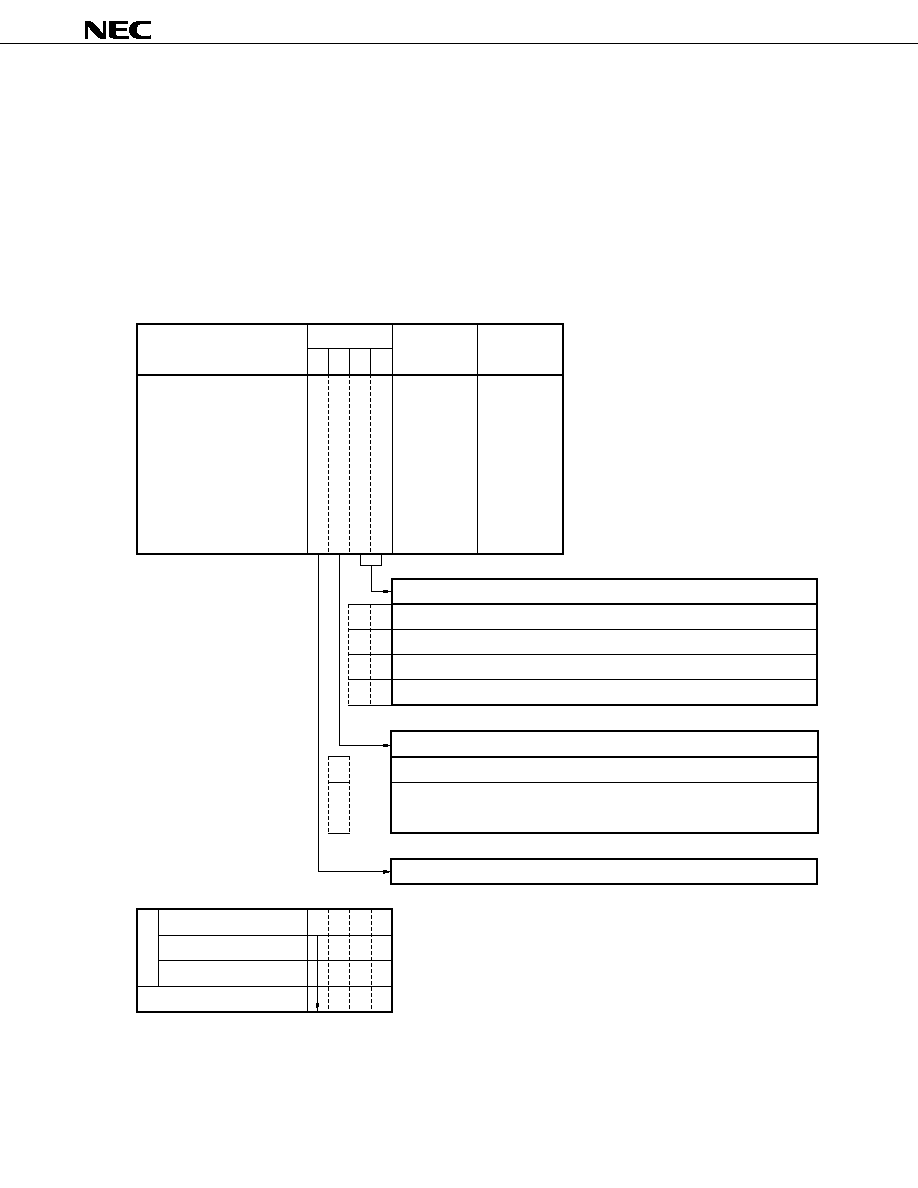
221
�
PD17704, 17705, 17707, 17708, 17709
16.2.3 Clock control block
The clock control block controls generation of a clock when the internal clock is used (master operation) and clock
output timing.
The frequency f
SC
of the internal clock is set by the SIO0CK1 and SIO0CK0 flags of the serial I/O0 clock selection
register.
Figure 16-4 shows the configuration of the serial I/O0 clock selection register.
The shift clock output from the clock control block is valid only for the master operation (SIO0MS flag = 1).
For the clock generation timing, refer to the description of each communication mode.
Figure 16-4. Configuration of Serial I/O0 Clock Selection Register
Name
Flag symbol
b
3
0
b
2
S
B
M
D
b
1
S
I
O
0
C
K
1
b
0
S
I
O
0
C
K
0
Address
0BH
Read/Write
R/W
Serial I/O0 clock selection
Power-ON reset
WDT&SP reset
CE reset
Clock stop
At reset
0
0
0
0
0
0
0
0
0
0
0
0
0
93.75 kHz
375.00 kHz
281.25 kHz
46.875 kHz
Selects internal shift clock frequency f
SC
of serial interface 0
Continues processing
Slave reception mode is set automatically if acknowledge signal is not
received (fixed to
"
1
"
when serial I/O is selected)
Selects operation mode during slave transmission of I
2
C bus
Fixed to
"
0
"
0
1
0
0
1
1
0
1
0
1

222
�
PD17704, 17705, 17707, 17708, 17709
16.2.4 Clock counter and start/stop detection block
The clock counter is a wrap-around counter that counts the rising edges of the clock.
Because this counter directly reads the status of the clock pin, whether the clock is an internal clock or external
clock cannot be identified.
The contents of the clock counter can be detected via the SIO0SF8 and SIO0SF9 flags of the serial I/O0 status
detection register, but cannot be directly read by program.
The start/stop detection block detects the start and stop conditions when the I
2
C bus mode is used.
The start and stop conditions are detected by the SBSTT and SBBSY flags of the serial I/O0 status detection
register.
Figure 18-5 shows the configuration of the serial I/O0 status detection register.
For the operation and timing chart of the clock counter, refer to the description of each communication mode.
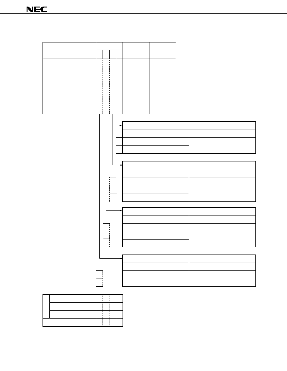
223
�
PD17704, 17705, 17707, 17708, 17709
Figure 16-5. Configuration of Serial I/O0 Status Detection Register
Name
Flag symbol
b
3
S
I
O
0
S
F
8
b
2
S
I
O
0
S
F
9
b
1
S
B
S
T
T
b
0
S
B
B
S
Y
Address
0DH
Read/Write
R
Serial I/O0 status detection
Power-ON reset
WDT&SP reset
CE reset
Clock stop
At reset
0
0
0
0
0
0
0
0
0
0
0
0
0
0
0
0
0
1
Detects stop condition
Detects start condition
Detects start /stop condition of I
2
C bus mode
0
1
0
1
0
1
I
2
C bus mode
Serial I/O mode
Retains
"
0
"
Detects rising of clock when value of
clock counter is
"
9
"
Detects start condition
Detects start condition and clock counter in I
2
C bus mode
I
2
C bus mode
Serial I/O mode
Retains
"
0
"
Detects rising of clock when value of
clock counter is next to
"
9
"
Value of clock counter is
"
9
"
Detects clock counter
I
2
C bus mode
Serial I/O mode
Retains
"
0
"
Detects rising of clock when value of clock counter is next to
"
8
"
Value of clock counter is
"
8
"
Detects clock counter
I
2
C bus mode
Serial I/O mode

224
�
PD17704, 17705, 17707, 17708, 17709
16.2.5 Presettable shift register 0
Presettable shift register 0 is an 8-bit shift register that writes serial out data and reads serial in data.
This register writes or reads data via data buffer.
It outputs the contents of the most significant bit (MSB) from the serial data I/O pin in synchronization with the falling
edge of the shift clock (during transmission operation), and reads data to the least significant bit (LSB) in synchronization
with the rising edge of the serial clock.
Figure 16-6 shows the configuration of the presettable shift register 0.
Figure 16-6. Configuration of Presettable Shift Register 0
Note
Data may be destroyed if the PUT or GET instruction is executed during serial communication. For details,
refer to 16.2.10 Causions on setting and reading data.
Name
b
3
b
2
b
1
Symbol Peripheral register
b
0
L
S
B
03H
Sets serial out data and reads serial in data
D7
D6
D5
D4
D3
D2
D1
D0
Serial out Serial in
Peripheral register
SIO0SFR
b
7
M
S
B
b
6
b
5
b
4
Presettable shift
register 0
Valid data
D7 D6 D5 D4 D3 D2 D1 D0
DBF3
Data buffer
Don't care
Transfer data
DBF2
Don't care
DBF1
DBF0
GET
Note
8
PUT
Note

225
�
PD17704, 17705, 17707, 17708, 17709
16.2.6 Wait control block and acknowledge control block
The wait control block keeps communication waiting or releases communication from the wait status.
The condition under which communication is kept waiting is set by the SIO0WRQ0 and 1 flags (bits 0 and 1 of serial
I/O0 wait control register).
Serial communication is started when the SIO0NWT flag (bit 2 of serial I/O0 wait control register) is set (released
from the wait status).
The communication status can be detected by the SIO0NWT flag.
When "0" is written to the SIO0NWT flag while communication is released from the wait status, the wait status is
set. This is called forced wait status.
The acknowledge control block outputs and detects an acknowledge signal in the I
2
C bus mode.
An acknowledge signal is set and read by the SBACK flag (bit 3 of serial I/O0 wait control register).
Figure 16-7 shows the configuration of the serial I/O0 wait control register.
Figure 16-8 shows the configuration of the serial I/O0 wait status judge register.

226
�
PD17704, 17705, 17707, 17708, 17709
Figure 16-7. Configuration of Serial I/O0 Wait Control Register
Name
Flag symbol
b
3
S
B
A
C
K
b
2
S
I
O
0
N
W
T
b
1
S
I
O
0
W
R
Q
1
b
0
S
I
O
0
W
R
Q
0
Address
0EH
Read/Write
R/W
Serial I/O0 wait control
Power-ON reset
WDT&SP reset
CE reset
Clock stop
At reset
0
0
0
0
0
0
0
0
0
0
0
0
0
0
0
0
0
1
0
1
0
0
1
1
No wait
Data wait
Acknowledge
wait
Address wait
Does not wait
Sets wait condition
0
1
0
1
I
2
C bus mode
Name
Serial I/O mode
Waits at falling edge of shift
clocks when value of clock
counter is
"
8
"
Waits at falling edge of shift
clock when value of clock
counter is
"
9
"
Waits at falling edge of clock
when value of clock counter
is
"
8
"
after detection of start
condition
Wait at rising edge of shift
clock when value of clock
counter is
"
8
"
Setting prohibited
Forced wait
Releases wait status
(serial communication starts)
Sets wait and detects wait status
When flag is written
When flag is read
Waits under condition of SIO0WRQ0
and 1 flags
Serial communication in progress
Reception
(SIO0TX = 0)
Transmission
(SIO0TX = 1)
Sets and detects acknowledge signal in I
2
C bus mode
I
2
C bus mode
Serial I/O mode
Retains
"
0
"
Detects acknowledge
of slave (acknowledge
is
"
0
"
)
Detects acknowledge
of slave (acknowledge
is
"
1
"
)
Outputs
"
0
"
as
acknowledge
Outputs
"
1
"
as
acknowledge

227
�
PD17704, 17705, 17707, 17708, 17709
Figure 16-8. Configuration of Serial I/O0 Wait Status Judge Register
Caution If a slave outputs a wait request while the master is operating, "0" is detected on the SIO0WSTT
flag. The SIO0NWT flag retains the status of 1.
Name
Flag symbol
b
3
0
b
2
0
b
1
0
b
0
S
I
O
0
W
S
T
T
Address
0AH
Read/Write
R
Serial I/O0 wait status judge
Power-ON reset
WDT&SP reset
CE reset
Clock stop
At reset
0
0
0
0
0
0
0
Waiting or requesting wait by slave
Serial communication in progress
Fixed to
"
0
"
Detects serial communication status
0
1

228
�
PD17704, 17705, 17707, 17708, 17709
16.2.7 Interrupt control block
The interrupt control block sets a condition under which an interrupt request is issued by the serial I/O0 interrupt
mode selection register.
When the interrupt request issuance condition is satisfied, the IRQSIO0 flag is set.
Change the interrupt request issuance condition while communication is in the wait status. If it is changed after
communication has been released from the wait status, an interrupt request may be issued as soon as the condition
has been changed.
Figure 16-9 shows the configuration of the serial I/O0 interrupt mode selection register.
Figure 16-9. Configuration of Serial I/O0 Interrupt Mode Selection Register
Notes 1. An interrupt request is issued if this mode is set when the value of the clock counter is "7".
2. An interrupt request is issued if this mode is set when the value of the clock counter is "8".
3. An interrupt request is issued if this mode is set when the SBSTT flag = 1 and the value of the clock
counter is "7".
4. An interrupt request is issued if this mode is set after the stop condition has been issued.
Name
Flag symbol
b
3
0
b
2
0
b
1
S
I
O
0
I
M
D
1
b
0
S
I
O
0
I
M
D
0
Address
0CH
Read/Write
R/W
Serial I/O0 interrupt mode
selection
Power-ON reset
WDT & SP reset
CE reset
Clock stop
At reset
0
0
0
0
0
0
0
0
0
0
Rising edge of shift clock when value
of clock counter reaches
"
7
"
Rising edge of shift clock when value
of clock counter reaches
"
8
"
Rising edge of shift clock when value
of clock counter reaches
"
7
"
after
detection of start condition
Note 3
When stop condition is detected
Note 4
Rising edge of shift clock when value
of clock counter reaches
"
7
"
Note 1
Rising edge of shift clock when value
of clock counter reaches
"
8
"
Note 2
Interrupt request is not issued
Sets interrupt request issuance condition
Fixed to
"
0
"
0
0
1
1
0
1
0
1
I
2
C bus mode
Serial I/O mode

229
�
PD17704, 17705, 17707, 17708, 17709
16.2.8 I
2
C bus mode
(1) Outline of I
2
C bus mode
In the I
2
C bus mode, communication is carried out with two pins, SCL and SDA.
The features of the I
2
C bus mode are as follows.
�
Communication can be controlled under the start/stop conditions and by the acknowledge signal for the
ninth clock.
�
Communication can be kept waiting by externally fixing the clock to low level with an N-ch open-drain pin.
(2) Timing chart
Figure 16-10 shows the timing chart.
Figure 16-10. Timing Chart in I
2
C Bus Mode
<1> Initial status (general-purpose input port)
<2> Generates start condition by general-purpose I/O port
<3> Sets transmission status of master
<4> Releases wait
<5> Wait timing when data wait status is set
<6> Wait timing when acknowledge wait status is set
<7> Sets general-purpose I/O port (releases serial operation mode)
<8> Generates stop condition by general-purpose I/O port
<9> Issues interrupt request when value of clock counter first reaches 7 after detection of start condition
<10> Issues interrupt request when value of clock counter reaches 7
<11> Issues interrupt request when value of clock counter reaches 8
<12> Issues interrupt request after stop condition is detected
Clock counter
Serial data
Shift clock
SIO0NWT
SIO0WSTT
SIO0SF8
SIO0SF9
SBSTT
SBBSY
Stop condition
<1>
<2>
<3>
<4>
1
D7
D6
D5
D1
D0
ACK
2
3
7
8
9
INT
9
0
8
7
6
2
1
0
<9>
<10>
<5>
<11>
<6>
<7>
<8>
<12>
Start condition

230
�
PD17704, 17705, 17707, 17708, 17709
(3) Operation of clock counter
The value of the clock counter is incremented from the initial value "0" each time the rising of the clock pin
has been detected.
In the I
2
C bus mode, the value of the clock counter returns to "0" after it has reached "9", and the clock counter
continues counting.
In the serial I/O mode, the value of the clock counter returns to "0" after it has reached "8", and the clock counter
continues counting.
The clock counter is also reset in the following cases.
�
At reset (power-ON reset, WDT&SP reset, CE reset)
�
On execution of clock stop instruction
�
On detection of start condition
�
If communication mode is changed from I
2
C bus mode to 2-wire or 3-wire serial I/O mode
(4) Wait operation and cautions
When the wait status is released, serial data is output (during transmission operation), and the wait status is
kept released until a condition (wait condition) set by the SIO0WRQ0 and 1 flags is satisfied.
When the wait condition is satisfied, the shift clock pin is made low, and the operations of the clock counter
and presettable shift register 0 are stopped.
If the forced wait status is specified while the wait status is released, the forced wait status is set at the falling
of the clock next to the one at which "0" has been written to the SIO0NWT flag.
Nothing is changed even if the wait status is released again after the wait status has been released once.
If the forced wait status is set in the wait status, one pulse of the shift clock is output.
In the I
2
C bus mode, do not set data wait conditions (SIOWRQ0 = 1, WIO0WRQ1 = 0) successively. This is
because, if the data wait condition is set two times in succession and the wait status is released, the wait status
is set as soon as the wait status has been released the second time.
While the device is operating as the master and if the level of the shift clock output pin is forcibly made low
externally while the pin outputs a high level (this is called a wait request by slave), the master is placed in the
wait status.
If this happens, the master resumes its operation when the wait request by the slave has been cleared.
(5) Interrupt request issuance timing
Interrupt request issuance timing can be selected by the SIO0IMD0 and 1 flags.
(6) Acknowledge block and its operation
The acknowledge block operates only in the I
2
C bus mode.
This block is used to output an acknowledge signal during a reception operation, or to detect an acknowledge
signal during a transmission operation.
During reception, the content of the SBACK flag is output to the serial data pin at the falling edge of the shift
clock when the value of the clock counter is "8".
Once data has been set to the SBACK flag during reception, the value of the data is retained.
During transmission, the status of the serial data pin is read to the SBACK flag at the rising edge of the shift
clock when the value of the clock counter reaches "9"
Figure 16-11 shows the acknowledge signal output and input operations.
During reception, set the acknowledge signal (setting of the SBACK flag) as soon as the wait status has been
released (by setting the SIO0NWT flag).

231
�
PD17704, 17705, 17707, 17708, 17709
This is because, even if only the SBACK flag is set, the SIO0NWT flag is also set because it is in the register
at the same address. If the wait status is set at this time, the wait status is released and one pulse of the shift
clock is output.
Figure 16-11. Acknowledge Output and Input Operations
Data input
Data
Hi-Z (D1)
Hi-Z (D0)
SBACK output
Hi-Z
Shift clock
7
8
9
Acknowledge output
At this time, wait status must
be released at the same time.
Data output
Data
D1 output
D0 output
ACK at reception
side
Shift clock
7
8
9
Acknowledge input
(a) During reception
(b) During transmission

232
�
PD17704, 17705, 17707, 17708, 17709
(7) Shift clock generation timing in I
2
C bus mode
(a) On releasing wait status from initial status
The initial status is the point where the master operation in the I
2
C bus mode is selected.
In the wait status, a low level is output to the shift clock pin.
Figure 16-12. Shift Clock Generation Timing in I
2
C Bus Mode (1/5)
Wait period
1/f
SC
Shift clock
Wait released
Initialization
1 : 1
(b) During wait operation
<1> Wait status under condition of SIO0WRQ0 and SIO0WRQ1 flags (normal operation)
Figure 16-12. Shift Clock Generation Timing in I
2
C Bus Mode (2/5)
Wait period
Wait released status
1/f
SC
Shift clock
Wait under condition of
SIO0WRQ1 and
SIO0WRQ0
Wait released
<2> If forced wait status is set in wait status
Nothing is affected.
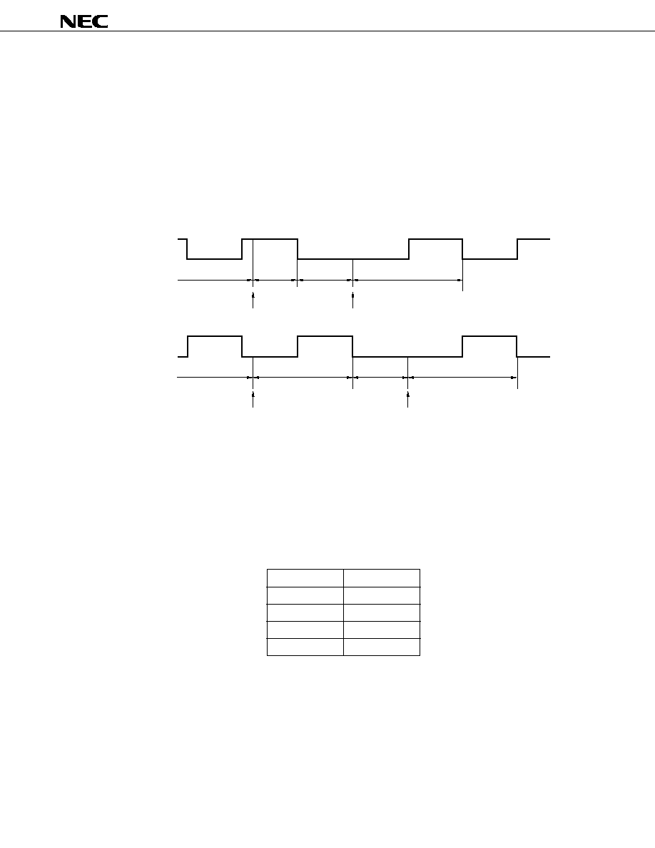
233
�
PD17704, 17705, 17707, 17708, 17709
<3> If forced wait status is set after wait status has been released
In this case, the wait status is set at the next falling edge of the clock after the one at which the forced
wait status was set.
When the forced wait status was set, however, the clock counter and presettable shift register 0 stop
operating.
If the forced wait status is set while the clock pin is low, the clock counter and presettable shift register
0 operate by 1 pulse. Because the internal clock counter and shift register do not operate at this
time, communication may not be performed normally even if the wait status is released again.
Figure 16-12. Shift Clock Generation Timing in I
2
C Bus Mode (3/5)
1/f
SC
Wait period
Wait pending
Wait released status
Shift clock
Shift clock
Wait period
1/f
SC
Wait pending
Wait released
Forced wait set by
SIO0NWT
Forced wait set by
SIO0NWT
Wait released
<4> If wait status is released after wait status has been released
Nothing is affected.
<5> If wait request is made by slave after wait status has been released
At this time, the clock is output 0 to 3.3
�
s after the wait request by the slave has been cleared.
The value of T in the figure below is as follows:
f
SC
T
93.75 kHz
666 ns
375.00 kHz
222 ns
281.25 kHz
222 ns
46.875 kHz
666 ns

234
�
PD17704, 17705, 17707, 17708, 17709
Figure 16-12. Shift Clock Generation Timing in I
2
C Bus Mode (4/5)
(c) During slave (external clock) operation
When the slave operation is specified the first time after application of supply voltage V
DD
, the SCK pin
waits for input of an external clock and the output pin goes into a high-impedance state.
If the SCL pin is externally made low at this time, it continues outputting a low level until the wait status
is released next time.
Figure 16-12. Shift Clock Generation Timing in I
2
C Bus Mode (5/5)
1/f
SC
Wait request by slave
Wait released status
Shift clock
Wait request by slave cleared
0-3.3 s
Wait request by slave
T
Shift clock
Wait request by slave cleared
T
�
0-3.3 s
�
Wait period (originally, Hi-Z)
I/O port
Wait released period
Shift clock
Slave is set
Wait released
(8) Start and stop conditions, and operations of SBSTT and SBBSY flags
The start/stop condition recognition timing is shown in Figure 16-13.
The SBSTT and SBBSY flags operate only in the I
2
C bus mode.
By detecting these flags, communication status of the other stations can be detected.
These flags operate regardless of whether the device operates as the master or slave, whether it performs
reception or transmission, and whether communication is in the wait status or released from the wait status.
These flags are "0" in the serial I/O mode.
For the operations of the SBSTT and SBBSY flags, refer to Figure 16-10 Timing Chart in I
2
C Bus Mode.

235
�
PD17704, 17705, 17707, 17708, 17709
Figure 16-13. Start/Stop Condition Recognition Timing
(a) Start condition recognition timing
SBSTT
Serial data pin
Shift clock pin
SBBSY
L
H
Detects falling of serial data pin
About 1 s
Start condition is assumed if shift clock pin
goes high about 1 s after serial data pin
has gone low.
L
H
H
L
L
H
�
�
(b) Stop condition recognition timing
SBSTT
Serial data pin
Shift clock pin
SBBSY
L
H
Detects rising of serial data pin
About 1 s
Stop condition is assumed if shift clock pin
goes high about 1 s after serial data pin
has gone high.
H
L
H
L
L
H
�
�
236
�
PD17704, 17705, 17707, 17708, 17709
16.2.9 Serial I/O mode
(1) Outline of serial I/O mode
In the serial I/O mode, communication is carried out by using two pins, SCL and SDA, or three pins, SCK0,
SO0, and SI0.
(2) Timing chart
Figure 16-14 shows the timing chart in the serial I/O mode.
Figure 16-14. Timing Chart in Serial I/O Mode
Clock counter
0
1
2
6
7
8
0
1
Serial data
La
D7
D6
D5
D1
D0
D7
Shift clock
SIO0NWT
SIO0WSTT
SIO0SF8
SIO0SF9
"0"
SBSTT
"0"
SBBSY
"0"
<1>
<2> <3>
<4>
1
1
2
3
7
8
<5>
INT<6>
<7>
<1> Initial status (general-purpose input port)
<2> Sets transmission status of master
<3> Releases wait status
<4> Wait timing when data wait status is set
<5> Releases wait status again
<6> Issues interrupt request when value of clock counter is 7
<7> Issues interrupt request when value of clock counter is 8

237
�
PD17704, 17705, 17707, 17708, 17709
(3) Operation of clock counter
The value of the clock counter is incremented from the initial value "0" each time the rising of the clock pin
has been detected.
The value of the clock counter returns to "0" after it has reached "8", and the clock counter continues counting.
The clock counter is also reset in the following cases.
�
At reset (power-ON reset, WDT&SP reset, CE reset)
�
On execution of clock stop instruction
�
If data is written to serial I/O0 wait control register
�
If communication mode is changed from 2-wire or 3-wire serial I/O mode to I
2
C bus mode
(4) Wait operation and Cautions
When the wait status is released, serial data is output (during transmission operation) at the falling of the next
clock, and the wait status is kept released until a condition (wait condition) set by the SIO0WRQ0 and 1 flags
is satisfied.
When the wait condition is satisfied, the shift clock pin is made high, and the operations of the clock counter
and presettable shift register 0 are stopped.
The value of the presettable shift register 0 cannot be read correctly if it is read while the wait status is released
and while the shift clock pin is high.
Correct data cannot be written to the presettable shift register 0 while the wait status is released and while
the shift clock pin is low.
If the forced wait status is specified while the wait status is released, the forced wait status is set as soon as
"0" has been written to the SIO0NWT flag.
The clock output wave is not affected even if the wait status is released again when it has been already released
once. Note, however, that the clock counter is reset.
(5) Interrupt request issuance timing
Interrupt request issuance timing can be selected by the SIO0IMD0 and 1 flags.
For details, refer to 16.2.7 Interrupt control block.
(6) Acknowledge block and its operation
The acknowledge block operates only in the I
2
C bus mode.
(7) Shift clock generation timing in serial I/O mode
(a) On releasing wait status from initial status
The initial status is the status when the internal clock operation in the serial I/O mode has been selected.
In the wait status, a high level is output to the shift clock pin.

238
�
PD17704, 17705, 17707, 17708, 17709
Figure 16-15. Shift Clock Generation Timing in Serial I/O Mode (1/4)
Wait period
1/f
SC
Shift clock
Wait released
Initialization
1 : 1
(b) When wait operation is performed
<1> If wait status is set under condition specified by SIO0WRQ0 and SIO0WRQ1 flags (normal
operation)
Figure 16-15. Shift Clock Generation Timing in Serial I/O Mode (2/4)
Shift clock
Wait released status
Wait period
1/f
SC
Wait released
Wait by SIO0WRQ1
and SIO0WRQ0
<2> If forced wait is set in wait status
Figure 16-15. Shift Clock Generation Timing in Serial I/O Mode (3/4)
Shift clock
Wait period
Wait period
Forced wait set by
SIO0NWT

239
�
PD17704, 17705, 17707, 17708, 17709
<3> If forced wait is set after wait status has been released
Figure 16-15. Shift Clock Generation Timing in Serial I/O Mode (4/4)
Wait period
Wait released status
1/f
SC
Forced wait by SIO0NWT
a
b
Wait released
Wait period
Wait released status
a + b = 1/2f
SC
a + b = 1/2f
SC
1/f
SC
Forced wait by SIO0NWT
a
b
Wait released
<4> If wait status is released when it has been already released once
The clock output waveform is not affected. However, note that the clock counter is reset.
(8) Operations of SBSTT and SBBSY flags
The SBSTT and SBBSY flags operate only in the I
2
C bus mode.
These flags remain "0" in the serial I/O mode.

240
�
PD17704, 17705, 17707, 17708, 17709
16.2.10 Cautions on setting and reading data
Data is set to the presettable shift register 0 by using the "PUT SIO0SFR, DBF" instruction.
To read the data of this register, the "GET DBF, SIO0SFR" instruction is used.
Set or read data of the register in the wait status. If the wait status is released, data may not be correctly set or
read depending on the status of the shift clock pin.
The following table shows the data setting and reading timing, and points to be noted.
Table 16-3. Reading and Writing Data of Presettable Shift Register 0 and Cautions
Status on Execution
Status of Shift
I
2
C Bus Mode
Serial I/O Mode
of PUT/GET
Clock Pin
Wait
Read (GET)
� I
2
C bus mode:
Normal read
Normal read
status
Write (PUT)
fixed to low
Normal write
Normal write
� Serial I/O mode:
Outputs contents of MSB when wait
Outputs contents of MSB when wait
fixed to high
status is released next time
status is released next time and shift
(during transmission)
clock pin goes low (during transmission)
Wait
Read (GET)
High level
Cannot be read normally
Cannot be read normally
released
Contents of SIO0SFR are lost
Contents of SIO0SFR are lost
status
Low level
Normal read
Normal read
Write (PUT)
High level
Normal write
Normal write
Outputs contents of MSB at falling
Outputs contents of MSB when PUT
of clock next to one at which PUT
instruction is executed.
instruction has been executed.
Clock counter is not reset
Clock counter is not reset
Low level
Cannot be read normally
Cannot be read normally
Contents of SIO0SFR are lost
Contents of SIO0SFR are lost
MSB
Data
Wait released
PUT SIO0SFR, DBF
Clock
H
L
1
0
MSB
Data
Wait released
PUT SIO0SFR, DBF
Clock
H
L
1
0
MSB
Data
Clock
H
L
1
0
PUT SIO0SFR, DBF
MSB
Data
PUT SIO0SFR, DBF
Clock
H
L
1
0

241
�
PD17704, 17705, 17707, 17708, 17709
16.2.11 Operation of serial interface 0
Tables 16-4 through 16-6 outlines the operations in each communication mode.
Table 16-4. Outline of Operation in I
2
C Bus Mode
Operation Mode
I
2
C Bus Mode
Slave operation (SIO0MS = 0)
Master operation (SIO0MS = 1)
Reception
Transmission
Reception
Transmission
Item
(SIO0TX = 0)
(SIO0TX = 1)
(SIO0TX = 0)
(SIO0TX = 1)
Status of
SDA/P0A3
When P0ABIO3 = 0
Outputs contents of
When P0ABIO3 = 0
Outputs contents of
each pin
Floating
SIO0SFR at falling of
Floating
SIO0SFR at falling of
Waits for input of
external clock
Waits for input of
internal clock
external data
regardless of
external data
regardless of P0ABIO3
When P0ABIO3 = 1
P0ABIO3
When P0ABIO3 = 1
General-purpose
General-purpose
output port
output port
Outputs content of
Outputs content of
output latch
output latch
SCL/P0A2
When P0ABIO2 = 0
Outputs internal clock regardless of P0ABIO2
Floating
Waits for input of external data
When P0ABIO2 = 1
General-purpose output port
Outputs content of output latch
Clock counter
Incremented at rising of SCL pin
Operation of
Output
Not output
Shifted from MSB
Not output
Shifted from MSB
presettable
each time SCL falls
each time SCL falls
shift register 0
and is output
and is output
Input
Shifted from LSB each time SCL rise and is input
Wait operation
In wait
SCL and SDA pins
SCL pin is floated
SCL pin outputs low
SCL pin outputs low
status
are floated
and SDA pin retains
level and SDA pin is
level and SDA pin
its status
floated
retains its status
Wait
SCL pin is floated
SCL pin is floated
SCL pin outputs
SCL pin outputs
released
and waits for input of
and waits for input of
internal clock.
internal clock.
external clock.
external clock.
SDA pin is floated
SDA pin outputs data
SDA pin is floated and
SDA pin outputs data
and waits for external
each time SCL pin falls
waits for external data
each time SCL pin falls
data
Acknowledge
ACK output at falling
ACK input at rising
ACK output at falling
ACK input at rising
of 8th clock
of 9th clock
of 8th clock
of 9th clock
� � � � � � � � � � � � � � � � � � � � � � � � � � � � � � � � � � � � � � � � � � � � � � � � � � � � � � � � � � � � � � � � � � � � � � � � � � � � � � � � �
� � � � � � � � � � � � � � � � � � � � � � � � � � � � � � � � � � � � � � � � � � � � � � � � � � � � � � � � � � � � � � � � � � � � � � � � � � � � � � � � �
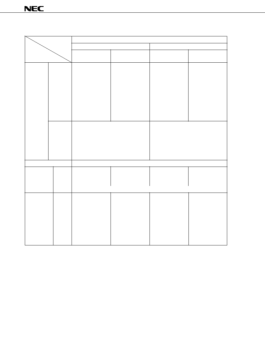
242
�
PD17704, 17705, 17707, 17708, 17709
Table 16-5. Outline of Operation in 2-Wire Serial I/O Mode
Operation Mode
2-Wire Serial I/O Mode
Slave operation (SIO0MS = 0)
Master operation (SIO0MS = 1)
Reception
Transmission
Reception
Transmission
Item
(SIO0TX = 0)
(SIO0TX = 1)
(SIO0TX = 0)
(SIO0TX = 1)
Status of
SDA/P0A3
When P0ABIO3 = 0
Outputs contents of
When P0ABIO3 = 0
Outputs contents of
each pin
Floating
SIO0SFR at falling of
Floating
SIO0SFR at falling of
Waits for input of
external clock
Waits for input of
internal clock
external data
regardless of P0ABIO3
external data
regardless of P0ABIO3
When P0ABIO3 = 1
When P0ABIO3 = 1
General-purpose
General-purpose
output port
output port
Outputs contents
Outputs contents of
of output latch
output latch
SCL/P0A2
When P0ABIO2 = 0
Outputs internal clock regardless of P0ABIO2
Floating
Waits for input of external data
When P0ABIO2 = 1
General-purpose output port
Outputs contents of output latch
Clock counter
Incremented at rising of SCL pin
Operation of
Output
Not output
Shifted from MSB
Not output
Shifted from MSB
presettable
each time SCL falls
each time SCL falls
shift register 0
and is output
and is output
Input
Shifted from LSB each time SCL rise and is input
Wait operation
In wait
SCL and SDA pins
SCL pin is floated
SCL pin outputs high
SCL pin outputs high
status
are floated
and SDA pin retains
level and SDA pin is
level and SDA pin
its status
floated
retains its status
Wait
SCL pin is floated
SCL pin is floated
SCL pin outputs
SCL pin outputs
released
and waits for input of
and waits for input
internal clock.
internal clock.
external clock.
of external clock.
SDA pin is floated and
SDA pin outputs data
SDA pin is floated and
SDA pin outputs data
waits for external data
each time SCL pin falls
waits for external data
each time SCL pin falls
� � � � � � � � � � � � � � � � � � � � � � � � � � � � � � � � � � � � � � � � � � � � � � � � � � � � � � � � � � � � � � � � � � � � � � � � � � � � � � � � �
� � � � � � � � � � � � � � � � � � � � � � � � � � � � � � � � � � � � � � � � � � � � � � � � � � � � � � � � � � � � � � � � � � � � � � � � � � � � � � � � �
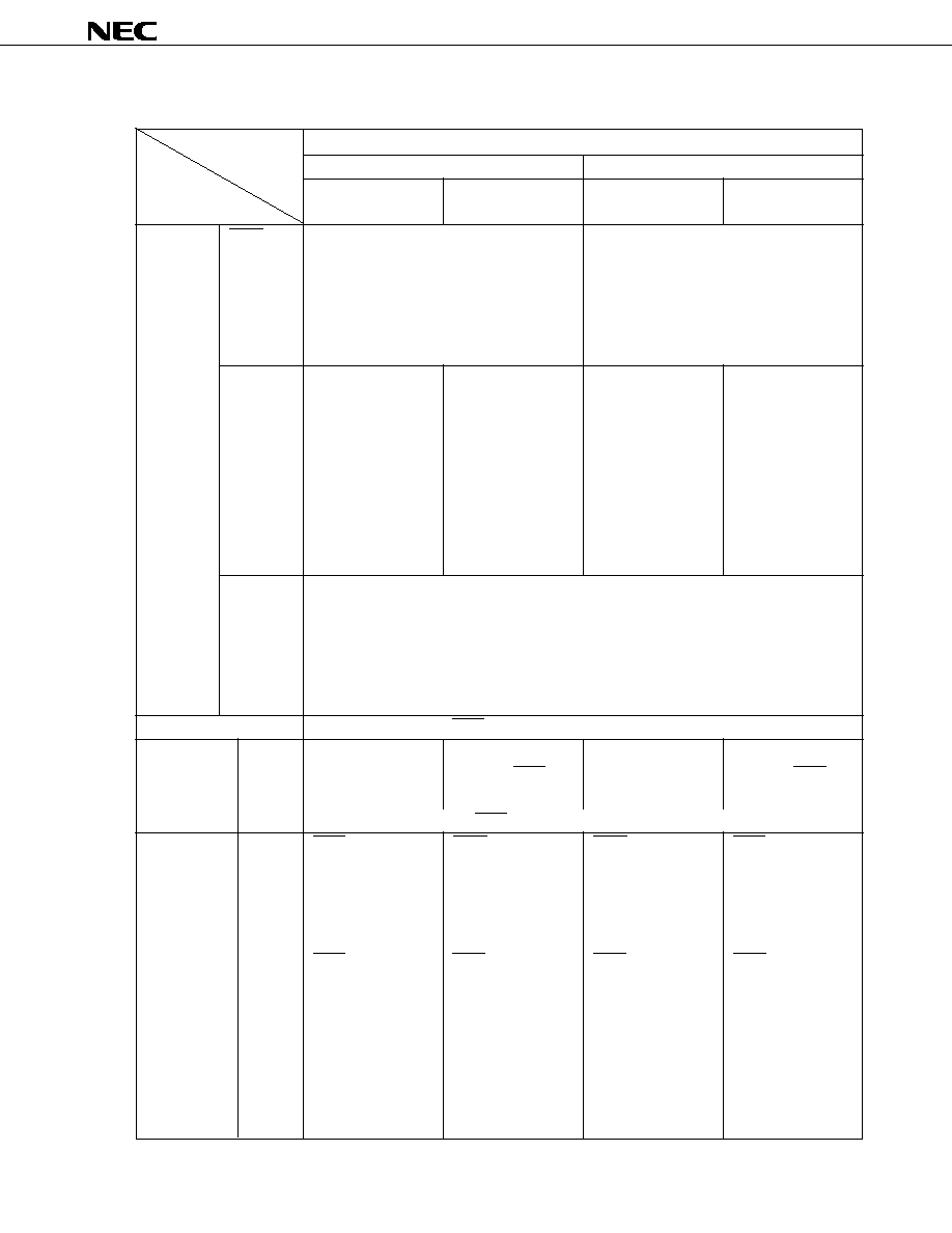
243
�
PD17704, 17705, 17707, 17708, 17709
Table 16-6. Outline of Operation in 3-Wire Serial I/O Mode
Operation Mode
3-Wire Serial I/O Mode
Slave operation (SIO0MS = 0)
Master operation (SIO0MS = 1)
Reception
Transmission
Reception
Transmission
Item
(SIO0TX = 0)
(SIO0TX = 1)
(SIO0TX = 0)
(SIO0TX = 1)
Status of
SCK0/P0A1
When P0ABIO1 = 0
Outputs internal clock regardless of P0ABIO1
each pin
Floating
Waits for input of external data
When P0ABIO1 = 1
General-purpose output port
Outputs contents of output latch
SO0/P0A0
When P0ABIO0 = 0
Outputs contents of
When P0ABIO0 = 0
Outputs contents of
General-purpose
SIO0SFR at falling
General-purpose
SIO0SFR at falling
input port
edge of external clock
input port
edge of internal
Floating
regardless of
Floating
clock regardless of
When P0ABIO0 = 1
P0ABIO0
When P0ABIO0 = 1
P0ABIO0
General-purpose
General-purpose
output port
output port
Outputs contents
Outputs contents
of output latch
of output latch
SI0/P0B3
When P0BBIO3 = 0
Floating
Waits for input of external data
When P0BBIO3 = 1
General-purpose output port
Outputs contents of output latch
Clock counter
Incremented at rising of SCK0 pin
Operation of
Output
Not output
Shifted from MSB
Not output
Shifted from MSB
presettable
each time SCK0 falls
each time SCK0 falls
shift register 0
and is output
and is output
Input
Shifted from LSB each time SCK0 falls and is input
Wait operation
In wait
SCK0 pin is floated.
SCK0 pin is floated.
SCK0 pin outputs high
SCK0 pin outputs high
status
SO0 pin as general-
SC0 pin retains its
level
level.
purpose port.
status.
SO0 pin as general-
SO0 pin retains its
SI0 pin is floated
SI0 pin is floated
purpose port.
status.
SI0 pin is floated
SI0 pin is floated
Wait
SCK0 pin is floated
SCK0 pin is floated
SCK0 pin is floated
SCK0 pin is floated
released
and waits for input of
and waits for input of
and waits for input of
and waits for input of
external clock.
external clock.
external clock.
external clock.
SO0 pin as general-
SO0 pin outputs data.
SO0 pin as general-
SO0 pin outputs data.
purpose port.
SI0 pin is floated and
purpose port.
SI0 pin is floated and
SI0 pin is floated and
waits for input of
SI0 pin is floated and
waits for input of
waits for input of
external data
waits for input of
external data
external data
external data
� � � � � � � � � � � � � � � � � � � � � � � � � � � � � � � � � � � � � � � � � � � � � � � � � � � � � � � � � � � � � � � � � � � � � � � � � � � � � � � � �
� � � � � � � � � � � � � � � � � � � � � � � � � � � � � � � � � � � � � � � � � � � � � � � � � � � � � � � � � � � � � � � � � � � � � � � � � � � � � � � � �

244
�
PD17704, 17705, 17707, 17708, 17709
16.2.12 Status of serial interface 0 at reset
(1) At power-ON reset
Each pin is set in the general-purpose input port mode.
The contents of presettable shift register 0 are undefined.
(2) At WDT&SP reset
Each pin is set in the general-purpose input port mode.
The contents of presettable shift register 0 are undefined.
(3) On execution of clock stop instruction
Each pin is set in the general-purpose I/O port mode and remains in the previous input or output mode.
The contents of presettable shift register 0 are undefined.
(4) At CE reset
Each pin is set in the general-purpose I/O port mode and remains in the previous input or output mode.
The contents of presettable shift register 0 are undefined.
(5) In halt status
Each pin retains its set status.
Output of the internal clock is stopped in the status where the HALT instruction is executed.
When an external clock is used, the operation continues even if the HALT instruction is executed.
Presettable shift register 0 retains the previous value.

245
�
PD17704, 17705, 17707, 17708, 17709
16.3 Serial Interface 1
16.3.1 Outline of serial interface 1
Figure 16-16 outlines the serial interface 1.
Serial interface 1 is used in the 3-wire serial I/O mode.
Figure 16-16. Outline of Serial Interface 1
SCK1/P0B2
SIO1CK0 and 1 flags
SIO1HIZ flag
Clock I/O
control block
Data I/O
control block
Wait signal
SIO1TS flag
4.5 MHz
Wait control
block
Clock control block
Clock counter
Count value: 8
IRQSIO1 flag
Presettable shift register 1
(SIO1SFR)
SO1/P0B1
SI1/P0B0
OUT
IN
Remarks 1.
SIO1CK1 and SIO1CK0 (bits 1 and 0 of serial I/O1 mode selection register: refer to Figure 16-17)
select a shift clock.
2.
SIO1TS (bit 3 of serial I/O1 mode selection register: refer to Figure 16-17) starts or stops communication
operation.
3.
SIO1HIZ (bit 2 of serial I/O1 mode selection register: refer to Figure 16-17) selects the function of
the SO1/P0B1 pin.
16.3.2 Clock I/O control block and data I/O control block
The clock I/O control block and data I/O control block control the transmission or reception operation of serial
interface 1 and selects a shift clock.
The internal clock (master) or external clock (slave) operation is selected by the SIO1CK0 and 1 flags.
The SIO1HIZ flag selects whether the SO1 pin is used as a serial data output pin.
The flags that control the clock I/O control block and data I/O control block are allocated to the serial I/O1 mode
selection register.
Figure 16-17 shows the configuration and function of the serial I/O1 mode selection register.
Table 16-7 shows the set status of each pin.
As shown in this table, flags that set the input or output mode of each pin must also be manipulated in addition
to the control flags of the serial interface, in order to set each pin .

246
�
PD17704, 17705, 17707, 17708, 17709
Figure 16-17. Configuration of Serial I/O1 Mode Selection Register
16.3.3 Clock counter
The clock counter is a wrap-around counter that counts the rising edges of the clock.
Because this counter directly reads the status of the clock pin, whether the clock is an internal clock or external
clock cannot be identified.
The contents of the clock counter cannot be directly read by software.
Name
Flag symbol
b
3
S
I
O
1
T
S
b
2
S
I
O
1
H
I
Z
b
1
S
I
O
1
C
K
1
b
0
S
I
O
1
C
K
0
Address
1DH
Read/Write
R/W
Serial I/O1 mode selection
Power-ON reset
WDT&SP reset
CE reset
Clock stop
At reset
0
1
0
1
0
0
0
0
External clock input
187.50 kHz
375.00 kHz
46.875 kHz
Selects shift clock of serial interface 1
0
0
0
0
0
0
0
0
0
0
1
1
General-purpose I/O port
Serail data output pin
Selects function of P0B1/SO1 pin
0
1
0
0
0
0
Stops (wait status)
Starts
Start or stops operation of serial communication
0
1

247
�
PD17704, 17705, 17707, 17708, 17709
Table 16-7. Status of Each Pin Set by Control Flag
Each Flag
Pin
Communication
mode
Setting of
SIO1 pin
Clock setting
Pin name
Set status of pin
S
I
O
1
H
I
Z
S
I
O
1
C
K
1
S
I
O
1
C
K
0
P
0
B
B
I
O
2
P
0
B
B
I
O
1
P
0
B
B
I
O
0
3-wire
serial I/O
External clock
SCK1/P0B2
0
0
0
Wait: General-purpose input port
Internal clock
0
1
1
Wait: General-purpose output port
Wait released: External clock input
Wait released: General-purpose output port
1
0
0
General-purpose input port
1
1
1
Wait: High-level output
Wait released: Internal clock output
General-
purpose port
Serial output
0
1
SO1/P0B1
SI1/P0B0
0
1
0
1
General-purpose input port
General-purpose output port
General-purpose input port
Serial data output
Serial data intput
General-purpose output port
0
1

248
�
PD17704, 17705, 17707, 17708, 17709
16.3.4 Presettable shift register 1
Presettable shift register 1 is an 8-bit shift register that writes serial out data and reads serial in data.
This register writes or reads data via data buffer.
It outputs the contents of the most significant bit (MSB) from the serial data I/O pin in synchronization with the falling
edge of the shift clock (during transmission operation), and reads data to the least significant bit (LSB) in synchronization
with the rising edge of the serial clock.
Figure 16-18 shows the configuration of the presettable shift register 1.
Figure 16-18. Configuration of Presettable Shift Register 1
Note
Data may be destroyed if the PUT or GET instruction is executed during serial communication. For details,
refer to 16.3.7 Cautions on setting and reading data.
16.3.5 Wait control block
The wait control block keeps communication waiting or releases communication from the wait status.
Serial communication is started when communication is released from the wait status by using the SIO1TS flag
of the serial I/O1 mode selection register.
Communication is set in the wait status eight clocks after the wait status has been released and communication
has been started.
The communication status can be detected by using the SIO1TS flag. To do so, detect the status of the SIO1TS
flag after setting this flag to "1".
If "0" is written to the SIO1TS flag when communication is released from the wait status, the wait status is set. This
wait status is called forced wait status.
For the configuration of the serial I/O1 mode selection register, refer to Figure 16-17.
Data buffer
DBF3
Don't care
DBF2
Don't care
Name
Presettable
shift register 1
Symbol
SIO1SFR
Peripheral
register
04H
DBF1
DBF0
b
3
b
2
b
1
b
0
L
S
B
b
7
M
S
B
b
6
b
5
b
4
Peripheral register
D3 D2 D1 D0
D7 D6 D5 D4
D7
D6
D5
D4
D3
D2
D1
D0
Serial out
Serial in
Transfer data
Valid data
Sets serial out data and reads serial in data
GET
Note
PUT
Note
8

249
�
PD17704, 17705, 17707, 17708, 17709
16.3.6 Operation of serial interface 1
(1) Timing chart
Figure 16-19 shows the timing chart.
Figure 16-19. Timing Chart of Serial Interface 1
Shift clock
Serial data
La
D7
1
2
1
0
<1>
<2>
<3>
INT <5>
<4>
2
6
7
8
0
1
3
7
8
1
D6
D5
D1
D0
D7
Clock counter
SIO1TS
<1> Initial status (general-purpose input port)
<2> Sets transmission status of master/releases wait status
<3> Wait timing
<4> Releases wait status again
<5> Interrupt issuance timing
(2) Operation of clock counter
The value of the clock counter is incremented from the initial value "0" each time the rising of the clock pin
has been detected.
The value of the clock counter returns to "0" after it has reached "8", and the clock counter continues counting.
The clock counter is also reset in the following cases.
�
At reset (power-ON reset, WDT&SP reset, CE reset)
�
On execution of clock stop instruction
�
If "0" is written to SIO1TS flag
(3) Wait operation and cautions
When the wait status is released, serial data is output (during transmission operation) at the falling of the next
clock, and the wait status is released at the eighth clock.
After eight clocks have been output, the shift clock pin is made high, and the operations of the clock counter
and presettable shift register 1 are stopped.
The value of the presettable shift register 1 cannot be read correctly if it is read while the wait status is released
and while the shift clock pin is high.
Correct data cannot be written to the presettable shift register 1 while the wait status is released and while
the shift clock pin is low.
If the forced wait status is specified while the wait status is released, the forced wait status is set as soon as
"0" has been written to the SIO1TS flag, and the clock counter is reset.
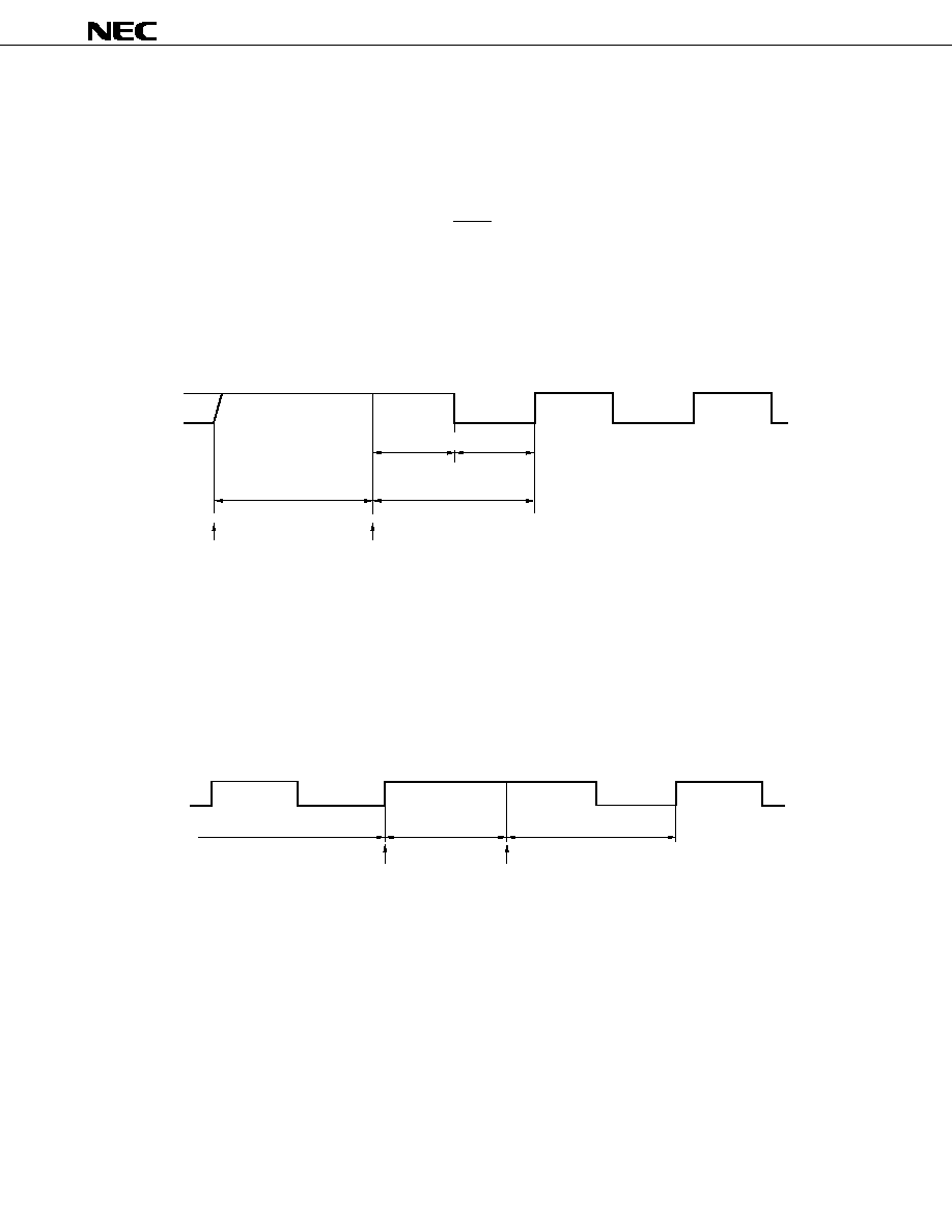
250
�
PD17704, 17705, 17707, 17708, 17709
(4) Interrupt request issuance timing
An interrupt request is issued at the rising of the shift clock when the value of the clock counter is "8".
(5) Shift clock generation timing
(a) On releasing wait status from initial status
The initial status is the status when the P0B2/SCK1 pin is set in the output mode and the internal clock
operation is selected.
In the wait status, a high level is output to the shift clock pin.
The wait status can be released and a clock can be selected at the same time.
Figure 16-20. Shift Clock Generation Timing of Serial Interface 1 (1/4)
1/f
SC
Wait status
Shift clock
Wait released
Initialization
1 : 1
(b) When wait operation is performed (normal operation)
<1> If wait status is set at the 8th clock (normal operation)
Figure 16-20. Shift Clock Generation Timing of Serial Interface 1 (2/4)
Shift clock
Wait
Wait release period
Wait period
1/f
SC
Wait released

251
�
PD17704, 17705, 17707, 17708, 17709
<2> If forced wait is set in wait status
Figure 16-20. Shift Clock Generation Timing of Serial Interface 1 (3/4)
<4> If wait status is released when it has been already released
The clock output waveform is not affected. The clock counter is not reset.
Shif clock
Wait period
Wait period
Forced wait set by
SIO1TS
<3> If forced wait is set after wait status has been released
Note that the clock counter is reset.
Figure 16-20. Shift Clock Generation Timing of Serial Interface 1 (4/4)
a
b
Wait status
Wait released status
1/f
SC
Shift clock
Shift clock
Forced wait by
SIO1TS
Wait released
a
b
Wait status
Wait released status
1/f
SC
a + b = 1/2f
SC
a + b = 1/2f
SC
Forced wait by
SIO1TS
Wait released

252
�
PD17704, 17705, 17707, 17708, 17709
16.3.7 Cautions on setting and reading data
Data is set to the presettable shift register 1 by using the "PUT SIO1SFR, DBF" instruction.
To read the data of this register, the "GET DBF, SIO1SFR" instruction is used.
Set or read data of the register in the wait status. If the wait status is released, data may not be correctly set or
read depending on the status of the shift clock pin.
The following table shows the data setting and reading timing, and points to be noted.
Table 16-8. Reading and Writing Data of Presettable Shift Register and Cautions
Status on Execution
Status of Shift
Serial I/O Mode
of PUT/GET
Clock Pin
Wait
Read (GET)
� External clock:
Normal write
status
Write (PUT)
floating
Normal write
� Internal clock:
Outputs contents of MSB when wait status is released next time and shift clock
output latch
pin falls (during transmission)
(always high)
Wait
Read (GET)
High level
Cannot be read normally
released
Contents of SIO1SFR are lost
status
Low level
Normal write
Write (PUT)
High level
Normal write
Outputs contents of MSB at which PUT instruction has been executed.
Clock counter is not reset
Low level
Cannot be read normally
Contents of SIO1SFR are lost
Data
MSB
Wait released
PUT SIO1SFR, DBF
Clock
H
L
1
0
Data
MSB
PUT SIO1SFR, DBF
Clock
H
L
1
0
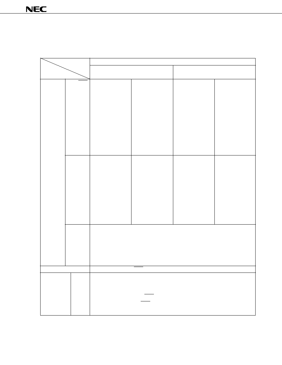
253
�
PD17704, 17705, 17707, 17708, 17709
16.3.8 Operation mode and operation of each part
Tables 16-9 outlines the operations of the 3-wire serial I/O mode.
Table 16-9. Outline of Operation of Serial Interface 1
Operation Mode
3-Wire Serial I/O Mode
Slave operation
Master operation
Item
(SIO1CK1 = SIO1CK0 = 0)
(SIO1CK1 = SIO1CK0 = other than 0)
Status of
P0B2/SCK1
During wait
Wait released
During wait
Wait released
each pin
(SIO1TS = 0)
(SIO1TS = 1)
(SIO1TS = 0)
(SIO1TS = 1)
When P0BBIO2 = 0
When P0BBIO2 = 0
When P0BBIO2 = 0
When P0BBIO2 = 0
Floating
Floating
Floating
Floating
General-purpose
Waits for input of
General-purpose
General-purpose
input port
external clock
input port
input port
When P0BBIO2 = 1
When P0BBIO2 = 1
When P0BBIO2 = 1
When P0BBIO2 = 1
General-purpose
General-purpose
General-purpose
Outputs internal clock
output port
output port
output port
Outputs contents of
Outputs contents
Outputs high level
output latch
of output latch
P0B1/SO1
SIO1HIZ = 0
SIO1HIZ = 1
SIO1HIZ = 0
SIO1HIZ = 1
When P0BBIO1 = 0
When P0BBIO1 = 0
When P0BBIO1 = 0
When P0BBIO1 = 0
Floating
Floating
Floating
Floating
General-purpose
General-purpose
General-purpose
General-purpose
input port
input port
input port
input port
When P0BBIO1 = 1
When P0BBIO1 = 1
When P0BBIO1 = 1
When P0BBIO1 = 1
General-purpose
Outputs data
General-purpose
Outputs data
output port
output port
Outputs contents of
Outputs contents of
output latch
output latch
P0B0/SI1
When P0BBIO0 = 0
Floating
Waits for input of serial data
When P0BBIO0 = 1
General-purpose output port
Outputs contents of output latch
Clock counter
Incremented at rising of SCK1 pin
Operation of
Output
SIO1HIZ = 0
presettable
Not output
shift register 1
SIO1HIZ = 1
Shifted from MSB each time SCK1 pin falls and is output
Input
Shifted from LSB each time SCK1 pin rises and is input.
SI1 pin outputs contents of output latch when P0BBIO0 = 1
� � � � � � � � � � � � � � � � � � � � � � � � � � � � � � � � � � � � � � � � � � � � � � � � � � � � � � � � � � � � � � � � � � � � � � � � �
� � � � � � � � � � � � � � � � � � � � � � � � � � � � � � � � � � � � � � � � � � � � � � � � � � � � � � � � � � � � � � � � � � � � � � � � �
� � � � � � � � � � � � � � � � � � � � � � � � � � � � � � � � � � � � � � � � � � � � � � � � � � � � � � � � � � � � � � � � � � � � � � � � � � � � � � � � �

254
�
PD17704, 17705, 17707, 17708, 17709
16.3.9 Status of serial interface 1 at reset
(1) At power-ON reset
Each pin is set in the general-purpose input port mode.
The contents of presettable shift register 1 are undefined.
(2) At WDT&SP reset
Each pin is set in the general-purpose input port mode.
The contents of presettable shift register 1 are undefined.
(3) On execution of clock stop instruction
Each pin is set in the general-purpose I/O port mode and remains in the previous input or output mode.
The contents of presettable shift register 1 are undefined.
(4) At CE reset
Each pin is set in the general-purpose I/O port mode and remains in the previous input or output mode.
The contents of presettable shift register 1 are undefined.
(5) In halt status
Each pin retains its set status.
Output of the internal clock is stopped in the status where the HALT instruction is executed.
When an external clock is used, the operation continues even if the HALT instruction is executed.
Presettable shift register 1 retains the previous contents.
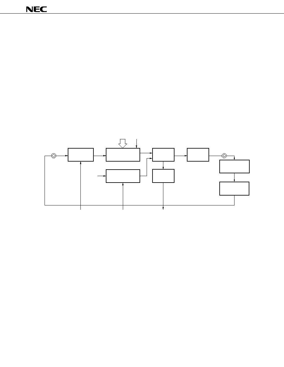
255
�
PD17704, 17705, 17707, 17708, 17709
17. PLL FREQUENCY SYNTHESIZER
The PLL (Phase Locked Loop) frequency synthesizer is used to lock a frequency in the MF (Medium Frequency),
HF (High Frequency), and VHF (Very High Frequency) to a constant frequency by means of phase difference comparison.
17.1 Outline of PLL Frequency Synthesizer
Figure 17-1 outlines the PLL frequency synthesizer. A PLL frequency synthesizer can be configured by connecting
an external lowpass filter (LPF) and voltage controlled oscillator (VCO).
The PLL frequency synthesizer divides a signal input from the VCOH or VCOL pin by using a programmable divider
and outputs a phase difference between this signal and a reference frequency from the EO0 and EO1 pins.
The PLL frequency synthesizer operates only while the CE pin is high. It is disabled when the CE pin is low. For
the details of the disabled status of the PLL frequency synthesizer, refer to 17.5 PLL Disabled Status.
Figure 17-1. Outline of PLL Frequency Synthesizer
Input select
block
Programmable
divider (PD)
Reference
frequency
generator
4.5 MHz
PLLSCNF flag
DBF
PLLRFCK3 flag
PLLRFCK2 flag
PLLRFCK1 flag
PLLRFCK0 flag
PLLUL flag
PLLMD1 flag
PLLMD0 flag
VCOH
VCOL
EO1
EO0
Phase
comparator
( -DET)
Charge
pump
Lowpass filter
(LPF)
Voltage controlled
oscillator (VCO)
Unlock FF
Note
Note
Note
External circuit
Remarks 1.
PLLMD1 and PLLMD0 (bits 1 and 0 of PLL mode selection register: refer to Figure 17-3) selects
a division mode of the PLL frequency synthesizer.
2.
PLLSCNF (bit 3 of PLL mode selection register: refer to Figure 17-3) selects the least significant
bit of the swallow counter.
3.
PLLRFCK3 through PLLRFCK0 (bits 3 through 0 of PLL reference frequency selection register: refer
to Figure 17-6) selects a reference frequency fr of the PLL frequency synthesizer.
4.
PLLUL (bit 0 of PLL unlock FF register: refer to Figure 17-9) detects the PLL unlock FF status.

256
�
PD17704, 17705, 17707, 17708, 17709
17.2 Input Selection Block and Programmable Divider
17.2.1 Configuration and function of input selection block and programmable divider
Figure 17-2 shows the configuration of the input selection block and programmable divider.
The input selection block selects an input pin and division mode of the PLL frequency synthesizer.
The VCOH or VCOL pin can be selected as the input pin.
The voltage on the selected pin is at the intermediate level (approx. 1/2 V
DD
). The pin not selected is internally
pulled down.
Because these pins are connected to an internal AC amplifier, cut the DC component of the input signal by
connecting a capacitor in series to the pin.
Direct division mode and pulse swallow mode can be selected as division modes.
The programmable divider divides the frequency of the input signal according to the value set to the swallow counter
and programmable counter.
The pin and division mode to be used are selected by the PLL mode selection register.
Figure 17-3 shows the configuration of the PLL mode selection register.
The value of the programmable divider is set by using the PLL data register via data buffer.
Figure 17-2. Configuration of Input Selection Block and Programmable Divider
Note
PLLSCNF flag
PLLMD1 flag
PLLMD0 flag
VCOH
VCOL
PLL disable signal
2-modulus prescaler
1/32, 1/33
Programmable counter
12 bits
f
N
-DET
Swallow counter
5 bits
4
16
12
DBF
PLL data register
12 bits
4 bits
R
F
Note
To
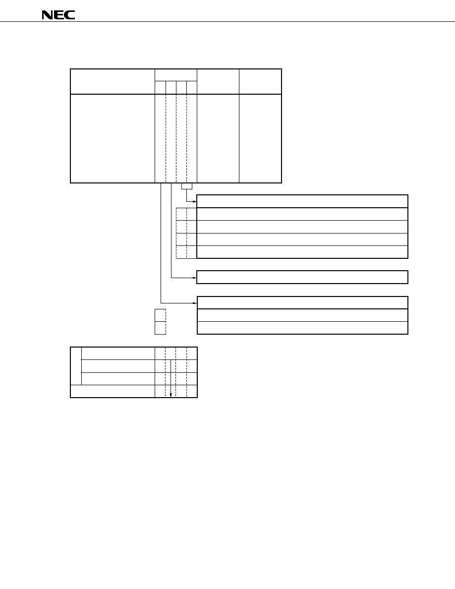
257
�
PD17704, 17705, 17707, 17708, 17709
Figure 17-3. Configuration of PLL Mode Selection Register
17.2.2 Outline of each division mode
(1) Direct division mode (MF)
In this mode, the VCOL pin is used.
The VCOH pin is pulled down.
In this mode, only the programmable counter is used for frequency division.
(2) Pulse swallow mode (HF)
In this mode, the VCOL pin is used.
The VCOH pin is pulled down.
In this mode, the swallow counter and programmable counter are used for frequency division.
Name
Flag symbol
b
3
P
L
L
S
C
N
F
b
2
0
b
1
P
L
L
M
D
1
b
0
P
L
L
M
D
0
Address
10H
Read/Write
R/W
PLL mode selection
Power-ON reset
WDT&SP reset
CE reset 1
Clock stop
At reset
0
1
0
1
0
0
0
0
Disables VCOL and VCOH pins
Direct division (VCOL pin, MF mode)
Pulse swallow (VCOH pin, VHF mode)
Pulse swallow (VCOL pin, HF mode)
Selects division mode of PLL frequency synthesizer
U
U
R
R
U: Undefined
R: Retained
0
0
0
1
1
Fixed to 0
0
0
0
0
Clears least significant bit to 0
Sets least significant bit to 1
Selects least significant bit of swallow counter
0
1

258
�
PD17704, 17705, 17707, 17708, 17709
(3) Pulse swallow mode (VHF)
In this mode, the VCOH pin is used.
The VCOL pin is pulled down.
In this mode, the swallow counter and programmable counter are used for frequency division.
(4) VCOL and VCOH pin disabled
In this mode, only the VCOL and VCOH pins are internally pulled down, but the other blocks operate.
17.2.3 Programmable divider and PLL data register
The programmable divider consists of a 5-bit swallow counter and a 12-bit programmable counter. Each counter
is a 17-bit binary down counter.
The programmable counter is allocated to the high-order 12 bits of the PLL data register, and the swallow counter
is allocated to the low-order 4 bits. Data are set to these counters via data buffer.
The least significant bit of the swallow counter sets data to the PLLSCNF flag of the control register.
The value by which the input signal frequency is to be divided is called "N value".
For how to set a division value (N value) in each division mode, refer to 17.6 Using PLL Frequency Synthesizer.
(1) PLL data register and data buffer
Figure 17-4 shows the relationships between the PLL data register and data buffer.
In the direct division mode, the high-order 12 bits of the PLL data register are valid, and all 17 bits of the register
are valid in the pulse swallow mode.
In the direct division mode, all 12 bits are used as a programmable counter.
In the pulse swallow mode, the high-order 12 bits are used as a programmable counter, and the low-order 5
bits are used as a swallow counter.
(2) Relationship between division value N of programmable divider and divided output frequency
The relationship between the value "N" set to the PLL data register and the signal frequency "f
N
" divided and
output by the programmable divider is as shown below.
For details, refer to 17.6 Using PLL Frequency Synthesizer.
(a) Direct division mode (MF)
f
IN
=
f
IN
N: 12 bits
N
(b) Pulse swallow mode (HF, VHF)
f
IN
=
f
IN
N: 17 bits
N

259
�
PD17704, 17705, 17707, 17708, 17709
Figure 17-4. Setting Division Value (N Value) of PLL Frequency Synthesizer
Note
The value of PLLSCNF flag is transferred when a write (PUT) instruction is executed to the PLL data register
(PLLR). Therefore, data must be set to the PLLSCNF flag before executing the write instruction to the PLL
data register.
Data buffer
DBF3
DBF2
Name
PLL data
register
Symbol
PLLR
Peripheral
address
42H
DBF1
DBF0
b
3
b
2
b
1
b
0
b
3
b
0
b
0
b
1
b
1
b
2
b
2
b
3
b
3
b
4
b
4
b
5
b
5
b
6
b
6
b
7
b
7
b
8
b
8
b
9
b
9
b
10
b
10
b
11
b
11
b
12
b
12
b
13
b
13
b
14
b
14
b
15
b
15
b
16
b
6
b
5
b
4
b
10
b
9
b
8
b
7
b
13
b
12
b
15
b
14
b
11
Peripheral register
PLL
N value data
(17 bits)
Direct division
mode
0
don't care
Setting prohibited
Division value N: N = x
Setting prohibited
Division value N: N = x
don't care
don't care
don't care
15 (00FH)
2
12
�1 (FFFH)
Pulse swallow
mode
Transfer data
Valid data
Sets high-order 16 bits of division value
Sets least significant bit of division value
Note
Name
PLL mode
selection
address
10H
b
3
P
L
L
S
C
N
F
P
L
L
M
D
1
P
L
L
M
D
0
0
b
2
b
1
b
0
Register file
GET
PUT
16
Sets division value (N value) of PLL
frequency synthesizer
x
0
1023 (3FFH)
2
17
�1 (1FFFFH)
x
don't care
16 (010H)
1024 (400H)

260
�
PD17704, 17705, 17707, 17708, 17709
17.3 Reference Frequency Generator
Figure 17-5 shows the configuration of the reference frequency generator.
The reference frequency generator generates the reference frequency "fr" of the PLL frequency synthesizer by
dividing the 4.5 MHz output of a crystal oscillator.
Thirteen frequencies can be selected as reference frequency fr: 1, 1.25, 2.5, 3, 5, 6.25, 9, 10, 12.5, 18, 20, 25,
and 50 kHz.
The reference frequency fr is selected by the PLL reference frequency selection register.
Figure 17-6 shows the configuration and function of the PLL reference frequency selection registerion.
Figure 17-5. Configuration of Reference Frequency Generator
PLLRFCK3 flag
PLLRFCK2 flag
PLLRFCK1 flag
PLLRFCK0 flag
MUX
1 kHz
1.25 kHz
2.5 kHz
25 kHz
50 kHz
OFF
PLL disable signal
To -DET
Divider
4.5 MHz

261
�
PD17704, 17705, 17707, 17708, 17709
Figure 17-6. Configuration of PLL Reference Frequency Selection Register
Remark
When the PLL frequency synthesizer is disabled by the PLL reference frequency selection register, the
VCOH and VCOL pins are internally pulled down. The EO1 and EO0 pins are floated.
Name
Flag symbol
b
3
P
L
L
R
F
C
K
3
b
2
P
L
L
R
F
C
K
2
b
1
P
L
L
R
F
C
K
1
b
0
P
L
L
R
F
C
K
0
Address
11H
Read/Write
R/W
PLL reference
frequency selection
Power-ON reset
WDT&SP reset
CE reset
Clock stop
At reset
0
0
0
0
0
0
0
0
1
1
1
1
1
1
1
1
1
1
1
1
0
1
0
1
0
1
0
1
0
1
0
1
0
1
0
1
1
1
1
1
1.25 kHz
2.5 kHz
5 kHz
10 kHz
6.25 kHz
12.5 kHz
25 kHz
50 kHz
3 kHz
9 kHz
18 kHz
Setting prohibited
1 kHz
20 kHz
Setting prohibited
PLL disable
Sets reference frequency f
r
of PLL frequency synthesizer
0
0
0
0
1
1
1
1
0
0
0
0
1
1
1
1
1
1
1
1
0
0
1
1
0
0
1
1
0
0
1
1
0
0
1
1
1
1
1
1

262
�
PD17704, 17705, 17707, 17708, 17709
17.4 Phase Comparator (
-DET), Charge Pump, and Unlock FF
17.4.1 Configuration of phase comparator, charge pump, and unlock FF
Figure 17-7 shows the configuration of the phase comparator, charge pump, and unlock FF.
The phase comparator compares the phase of the divided frequency "f
N
" output by the programmable divider with
the phase of the reference frequency "fr" output by the reference frequency generator, and outputs an up (UP) or down
(DW) request signal.
The charge pump outputs the output of the phase comparator from an error out pin (EO1 and EO0 pins).
The unlock FF detects the unlock status of the PLL frequency synthesizer.
17.4.2 through 17.4.4 describe the operations of the phase comparator, charge pump, and unlock FF.
Figure 17-7. Configuration of Phase Comparator, Charge Pump, and Unlock FF
Unlock FF
PLLUL flag
UP
f
r
f
N
Charge pump
EO1
EO0
Reference frequency
generator
Programmable
divider
DW
PLL disable signal
Phase comparator
( - DET)
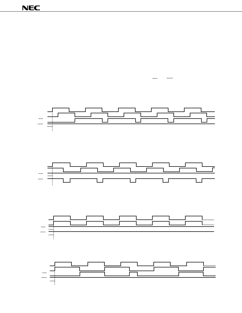
263
�
PD17704, 17705, 17707, 17708, 17709
17.4.2 Function of phase comparator
As shown in Figure 17-7, the phase comparator compares the phases of the divided frequency "f
N
" output by the
programmable divider and the reference frequency "fr", and outputs an up or down request signal.
If the divided frequency f
N
is lower than reference frequency fr, the up request signal is output. If f
N
is higher than
fr, the down request signal is output.
Figure 17-8 shows the relationship between reference frequency fr, divided frequency f
N
, up request signal, and
down request signal.
When the PLL frequency synthesizer is disabled, neither the up request nor the down request signal is output.
The up and down request signals are input to the charge pump and unlock FF, respectively.
Figure 17-8. Relationship between fr, f
N
, UP, and DW
(a) If f
N
lags behind fr
(b) If f
N
leads fr
(c) If f
N
and fr are in phase
(d) If f
N
is lower than fr
f
r
f
N
UP
DW
f
r
f
N
UP
DW
f
r
f
N
UP
DW
f
r
f
N
UP
DW

264
�
PD17704, 17705, 17707, 17708, 17709
17.4.3 Charge pump
As shown in Figure 17-7, the charge pump outputs the up request and down request signals output by the phase
comparator, from the error out pins (EO1 and EO0 pins).
Therefore, the relationship between the output of the error out pins, divided frequency f
N
and reference frequency
fr is as follows:
Where reference frequency fr > divided frequency f
N
: Low-level output
Where reference frequency fr < divided frequency f
N
: High-level output
Where reference frequency fr = divided frequency f
N
: Floating
17.4.4 Unlock FF
As shown in Figure 17-7, the unlock FF detects the unlock status of the PLL frequency synthesizer from the up
request and down request signals of the phase comparator.
Because either the up request or down request signal is low in the unlock status, the unlock status is detected by
this low-level signal.
In the unlock status, the unlock FF is set to 1.
The unlock FF is set in the cycle of the reference frequency fr selected at that time. When the contents of the PLL
unlock FF register are read (by the PEEK instruction), the unlock FF is reset (Read & Reset).
Therefore, the unlock FF must be detected in a cycle longer than cycle 1/fr of the reference frequency fr.
The status of the unlock FF is detected by the PLL unlock FF register. Figure 17-9 shows the configuration of the
PLL unlock FF register.
Because this register is a read-only register, its contents can be read to the window register by the "PEEK"
instruction.
Because the unlock FF is set in a cycle of the reference frequency fr, the contents of the PLL unlock FF register
are read to the window register in a cycle longer than cycle 1/fr of the reference frequency.
The delay time of the up and down request signals of the phase comparator are fixed to 0.8 to 1.0
�
s.

265
�
PD17704, 17705, 17707, 17708, 17709
Figure 17-9. Configuration of PLL Unlock FF Register
Name
Flag symbol
b
3
0
b
2
0
b
1
0
b
0
P
L
L
U
L
Address
12H
Read/Write
R & Reset
PLL unlock FF
Power-ON reset
WDT&SP reset
CE reset
U: Undefined
R: Retained
Clock stop
At reset
0
1
U
U
R
R
Unlock FF = 0: PLL locked status
Unlock FF = 1: PLL unlocked status
Fixed to 0
Detects status of unlock FF
0
0
0

266
�
PD17704, 17705, 17707, 17708, 17709
17.5 PLL Disabled Status
The PLL frequency synthesizer stops (is disabled) while the CE pin is low.
Likewise, it also stops when PLL disabled status is selected by the PLL reference frequency register (RF address
11H).
Table 17-1 shows the operation of each block in the PLL disabled status.
When the VCOL and VCOH pins are disabled by the PLL mode selection register, only the VCOL and VCOH pins
are internally pulled down, and the other blocks operate.
Because the PLL frequency selection register and PLL mode selection register are not initialized at CE reset (hold
the previous status), these registers return to the previous status when the CE pin has gone low, the PLL frequency
synthesizer has been disabled, and then CE pin has gone high.
To disable the PLL frequency synthesizer at CE reset, initialize these registers in software.
At power-ON reset, the PLL frequency synthesizer is disabled.
Table 17-1. Operation of Each Block under Each PLL Disable Condition
Condition
CE Pin = Low Level
CE Pin = High Level
(PLL disabled)
PLL reference frequency
PLL mode selection
selection register = 1111B
register = 0000B
Each Block
(PLL disabled)
(VCOH and VCOL disabled)
VCOL, VCOH pins
Internally pulled down
Internally pulled down
Internally pulled down
Programmable divider
Division stopped
Division stopped
Operates
Reference frequency generator
Output stopped
Output stopped
Operates
Phase comparator
Output stopped
Output stopped
Operates
Charge pump
Error out pins are floated
Error out pins are floated
Operates.
However, usually outputs
low level because no
signal is input

267
�
PD17704, 17705, 17707, 17708, 17709
17.6 Using PLL Frequency Synthesizer
To control the PLL frequency synthesizer, the following data is necessary.
(1) Division mode
: Direct division (MF), pulse swallow (HF, VHF)
(2) Pins used
: VCOL and VCOH pins
(3) Reference frequency : fr
(4) Division value
: N
17.6.1 through 17.6.3 below describe how to set PLL data in each division mode (MF, HF, and VHF).
17.6.1 Direct division mode (MF)
(1) Selecting division mode
Select the direct division mode by using the PLL mode selection register.
(2) Pins used
The VCOL pin is enabled to operate when the direct division mode is selected.
(3) Selecting reference frequency fr
Select the reference frequency by using the PLL reference frequency selection register.
(4) Calculation of division value N
Calculate N as follows:
N =
f
VCOL
fr
f
VCOL
: Input frequency of VCOL pin
fr
: Reference frequency
(5) Example of setting PLL data
How to set data to receive broadcasting in the following MW band is described below.
Reception frequency
: 1422 kHz (MW band)
Reference frequency
: 9 kHz
Intermediate frequency : +450 kHz
Division value N is calculated as follows:
N =
f
VCOL
=
1422 + 450
= 208 (decimal)
fr
9
= 0D0H (hexadecimal)
Set data to the PLL data register, PLL mode selection register, and PLL reference frequency selection register
as follows:

268
�
PD17704, 17705, 17707, 17708, 17709
Notes 1. PLLSCNF flag
2. don't care
PLL data register (PLLR)
0 0 0 0
0
0 0 0 0
0
don't care
1 1 0 1
D
PLL mode
selection
register
PLL reference
frequency
selection register
Note 1
Note 2
1 1 0 1
9 kHz
0 0 1
MF
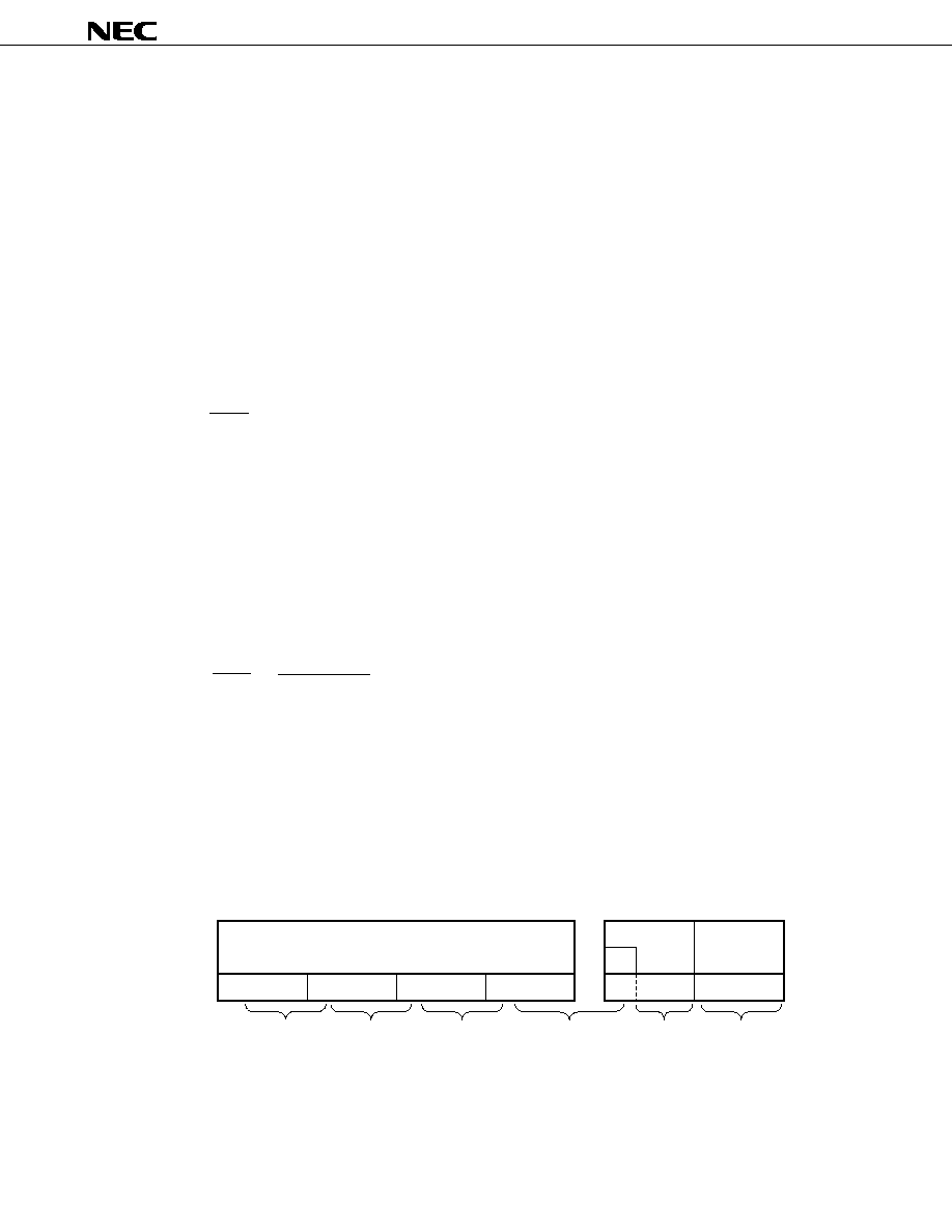
269
�
PD17704, 17705, 17707, 17708, 17709
17.6.2 Pulse swallow mode (HF)
(1) Selecting division mode
Select the pulse swallow mode by using the PLL mode selection register.
(2) Pins used
The VCOL pin is enabled to operate when the pulse swallow mode is selected.
(3) Selecting reference frequency fr
Select the reference frequency by using the PLL reference frequency selection register.
(4) Calculation of division value N
Calculate N as follows:
N =
f
VCOL
fr
f
VCOL
: Input frequency of VCOL pin
fr
: Reference frequency
(5) Example of setting PLL data
How to set data to receive broadcasting in the following SW band is described below.
Reception frequency
: 25.50 MHz (SW band)
Reference frequency
: 5 kHz
Intermediate frequency : +450 kHz
Division value N is calculated as follows:
N =
f
VCOL
=
25500 + 450
= 5190 (decimal)
fr
5
= 1446H (hexadecimal)
Set data to the PLL data register, PLL mode selection register, and PLL reference frequency selection register
as follows:
Caution The division value N is 17 bits long when the pulse swallow mode is selected, and the least
significant bit of the swallow counter is the bit 3 of the PLL mode selection register (PLLSCNF).
To set "1446H" as the division value N, the value to be actually set to the PLL data register
is "0A23H".
Note
PLLSCNF flag
PLL data register (PLLR)
0 0 0 0
0 0 1 0 0 0 1 1
1 0 1 0
PLL mode
selection
register
PLL reference
frequency
selection register
Note
0
0 0 1 0
0 1 1
5 kHz
HF
6
4
4
1

270
�
PD17704, 17705, 17707, 17708, 17709
17.6.3 Pulse swallow mode (VHF)
(1) Selecting division mode
Select the pulse swallow mode by using the PLL mode selection register.
(2) Pins used
The VCOH pin is enabled to operate when the pulse swallow mode is selected.
(3) Selecting reference frequency fr
Select the reference frequency by using the PLL reference frequency selection register.
(4) Calculation of division value N
Calculate N as follows:
N =
f
VCOH
fr
f
VCOH
: Input frequency of VCOH pin
fr
: Reference frequency
(5) Example of setting PLL data
How to set data to receive broadcasting in the following FM band is described below.
Reception frequency
: 98.15 MHz (FM band)
Reference frequency
: 50 kHz
Intermediate frequency : +10.7 MHz
Division value N is calculated as follows:
N =
f
VCOH
=
98.15 + 10.7
= 2177 (decimal)
fr
0.050
= 0881H (hexadecimal)
Set data to the PLL data register, PLL mode selection register, and PLL reference frequency selection register
as follows:
Caution The division value N is 17 bits long when the pulse swallow mode is selected, and the least
significant bit of the swallow counter is the bit 3 of the PLL mode selection register (PLLSCNF).
To set "0881H" as the division value N, the value to be actually set to the PLL data register
is "0440H".
PLL data register (PLLR)
0 0 0 0
0 1 0 0 0 0 0 0
0 1 0 0
PLL mode
selection
register
PLL reference
frequency
selection register
Note
1
0 1 0
50 kHz
VHF
1
8
8
0
0 1 1 1
Note
PLLSCNF flag

271
�
PD17704, 17705, 17707, 17708, 17709
Note that data must be set to the PLLSCNF flag before a write (PUT) instruction is executed to the PLL data
register (PLLR).
Example
SET1
PLLSCNF
MOV
DBF0, #0
MOV
DBF1, #4
MOV
DBF2, #4
PUT
PLLR, DBF
17.7 Status at Reset
17.7.1 At power-ON reset
The PLL frequency synthesizer is disabled because the PLL reference frequency selection register is initialized
to 1111B.
17.7.2 At WDT&SP reset
The PLL frequency synthesizer is disabled because the PLL reference frequency selection register is initialized
to 1111B.
17.7.3 On execution of clock stop instruction
The PLL frequency synthesizer is disabled because the PLL reference frequency selection register is initialized
to 1111B.
17.7.4 At CE reset
The PLL frequency synthesizer is disabled because the PLL reference frequency selection register is initialized
to 1111B.
17.7.5 In halt status
The set status is retained if the CE pin is high.

272
�
PD17704, 17705, 17707, 17708, 17709
18. FREQUENCY COUNTER
18.1 Outline of Frequency Counter
Figure 18-1 outlines the frequency counter.
The frequency counter has an IF counter function to count the intermediate frequency (IF) of an external input signal
and an external gate counter (FCG: Frequency Counter for external Gate signal) to detect the pulse width of an external
input signal.
The IF counter function counts the frequency input to the P1C0/FMIFC or P1C1/AMIFC pin at fixed intervals (1
ms, 4 ms, 8 ms, or open) by using a 16-bit counter.
The external gate counter function counts the frequency of the internal clock (1 kHz, 100 kHz, 900 kHz) from the
rising to the falling of the signal input to the P2A1/FCG1 or P2A0/FCG0 pin.
The IF counter and external gate counter functions cannot be used at the same time.
Figure 18-1. Outline of Frequency Counter
I/O selection
block
Gate time
control block
Start/stop control
block
IF counter
(16 bits)
P2A1/FCG1
FCGCH1 flag
FCGCH0 flag
IFCCK1 flag
IFCCK0 falg
IFCSTRT flag
DBF
IFCGOSTT flag
IFCRES flag
IFCMD1 flag
IFCMD0 flag
P2A0/FCG0
P1C0/FMIFC
P1C1/AMIFC
Remarks 1.
FCGCH1 and FCGCH0 (bits 1 and 0 of FCG channel selection register: refer to Figure 18-4) select
the pin used for the external gate counter function.
2.
IFCMD1 and IFCMD0 (bits 3 and 2 of IF counter mode selection register: refer to Figure 18-3) select
the IF counter or external gate counter function.
3.
IFCCK1 and IFCCK0 (bits 1 and 0 of IF counter mode selection register: refer to Figure 18-3) select
the gate time of the IF counter function and the reference frequency of the external gate counter
function.
4.
IFCSTRT (bit 1 of IF counter control register: refer to Figure 18-6) control starting of the IF counter
and external gate counter functions.
5.
IFCGOSTT (bit 0 of IF counter gate status detection register: refer to Figure 18-7) detects opening/
closing the gate of the IF counter function.
6.
IFCRES (bit 0 of IF counter control register: refer to Figure 18-6) reset the count value of the IF
counter.

273
�
PD17704, 17705, 17707, 17708, 17709
18.2 Input/Output Selection Block and Gate Time Control Block
Figure 18-2 shows the configuration of the input/output selection block and gate time control block.
The input/output selection block consists of an IF counter input selection block and FCG I/O selection block.
The IF counter input selection block selects whether the frequency counter is used as an IF counter or an external
gate counter, by using the IF counter mode register. When the frequency counter is used as the IF counter, either
P1C0/FMIFC or P1C1/AMIFC pin and a count mode are selected. The pin not used for the IF counter is used as a
general-purpose input port pin.
The FCG I/O selection block selects the P2A1/FCG1 or P2A0/FCG0 pin by using the FCG channel selection
register, when the frequency counter is used as the external gate counter. The pin not used is used as a general-
purpose I/O port pin.
When using the frequency counter as the external gate counter, the pin to be used must be set in the input mode
by using the port 2A bit I/O selection register. This is because the pin is set in the general-purpose output port mode
if it is set in the output mode even if the external gate counter function is selected by the IF counter mode selection
register and FCG channel selection register.
The gate time control block selects gate time by using the IF counter mode selection register when the frequency
counter is used as the IF counter, or a count frequency when the frequency counter is used as the external gate counter.
Figure 18-3 shows the configuration of the IF counter mode selection register.
Figure 18-4 shows the configuration of the FCG channel selection register.
Figure 18-2. Configuration of I/O Selection Block and Gate Time Control Block
1/2
P2A1/FCG1
P2A0/FCG0
P1C0/FMIFC
P1C1/AMIFC
Input port
FMIFC
AMIFC
Gate signal
generator
Frequency generator
Selector
Frequency
Gate signal
To start/stop control
block
I/O port
FCGCH1 flag
FCGCH0 flag
IFCMD1 flag
IFCMD0 flag
FCG
IFCCK1 flag
IFCCK0 flag
Selector
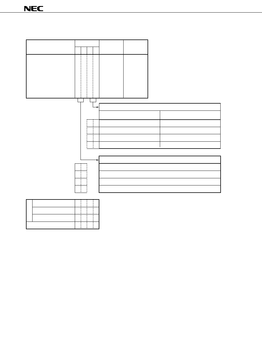
274
�
PD17704, 17705, 17707, 17708, 17709
Figure 18-3. Configuration of IF Counter Mode Selection Register
Caution The IF counter and external gate counter functions cannot be used at the same time.
Name
Flag symbol
b
3
I
F
C
M
D
1
b
2
I
F
C
M
D
0
b
1
I
F
C
C
K
1
b
0
I
F
C
C
K
0
Address
22H
Read/Write
R/W
IF counter mode selection
Power-ON reset
WDT&SP reset
CE reset
Clock stop
At reset
0
1
0
1
0
0
0
0
1 ms
4 ms
8 ms
Open
1 kHz
100 kHz
900 kHz
Setting prohibited
Selects gate time of IF counter and reference frequency of external gate counter
Gate time of IF counter
Reference frequency of
external gate counter
0
0
0
0
0
0
0
0
0
0
1
1
0
0
0
0
0
1
0
1
External gate counter (FCG)
IF counter (AMIFC pin, AMIF count mode)
IF counter (FMIFC pin, FMIF count mode, 1/2 division)
IF counter (FMIFC pin, AMIF count mode)
Selects function of IF counter or external gate counter
0
0
1
1
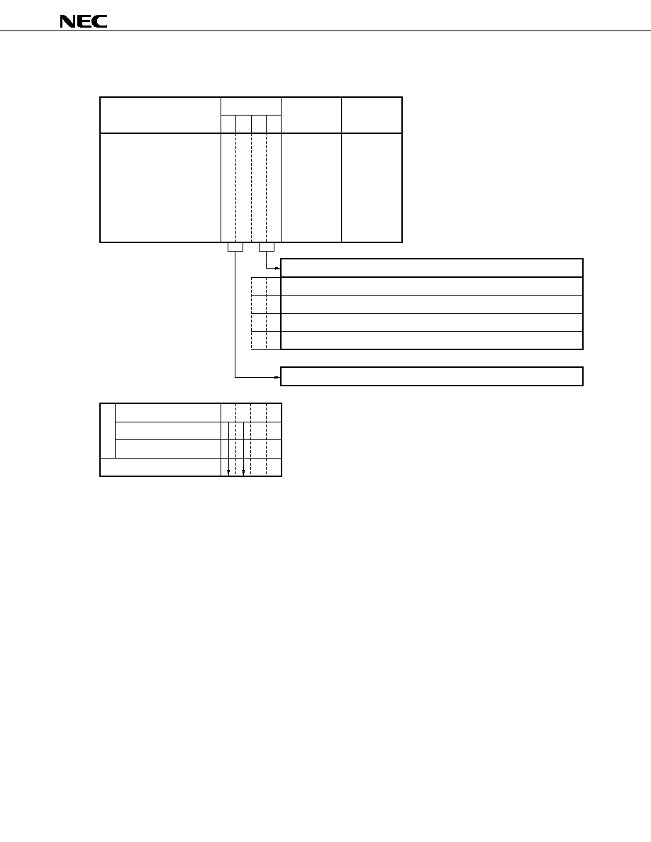
275
�
PD17704, 17705, 17707, 17708, 17709
Figure 18-4. Configuration of FCG Channel Selection Register
Name
Flag symbol
b
3
0
b
2
0
b
1
F
C
G
C
H
1
b
0
F
C
G
C
H
0
Address
20H
Read/Write
R/W
FCG channel selection
Power-ON reset
WDT&SP reset
CE reset
Clock stop
At reset
0
1
0
1
0
0
0
0
FCG not used (general-purpose I/O port)
P2A0/FCG0 pin
P2A1/FCG1 pin
Setting prohibited
Fixed to 0
Selects pin used for FCG
0
0
0
0
1
1
0
0
0
0

276
�
PD17704, 17705, 17707, 17708, 17709
18.3 Start/Stop Control Block and IF Counter
18.3.1 Configuration of start/stop control block and IF counter
Figure 18-5 shows the configuration of the start/stop control block and IF counter.
The start/stop control block starts the frequency counter or detects the end of counting.
The counter is started by the IF counter control register.
The end of counting is detected by the IF counter gate status detection register. When the external gate counter
function is used, however, the end of counting cannot be detected by the IF counter gate status detection register.
Figure 18-6 shows the configuration of the IF counter control register.
Figure 18-7 shows the configuration of the IF counter gate status detection register.
18.3.2 and 18.3.3 describe the gate operation when the IF counter function is selected and that when the external
gate counter function is selected.
The IF counter is a 16-bit binary counter that counts up the input frequency when the IF counter function or external
gate counter function is selected.
When the IF counter function is selected, the frequency input to a selected pin is counted while the gate is opened
by an internal gate signal. The frequency count is counted without alteration in the AMIF count mode. In the FMIF
counter mode, however, the frequency input to the pin is halved and counted.
When the external gate counter function is selected, the internal frequency is counted while the gate is opened
by the signal input to the pin.
When the IF counter counts up to FFFFH, it remains at FFFFH until reset.
The count value is read by the IF counter data register (IFC) via data buffer.
The count value is reset by the IF counter control register.
Figure 18-8 shows the configuration of the IF counter data register.
Figure 18-5. Configuration of Start/Stop Control Block and IF Counter
Start/Stop
control
IF counter
(16 bits)
16
IF counter data
register (IFC)
DBF
IFCSTRT flag
IFCRES flag
IFCGOSTT flag
Gate signal
Frequency
From gate time
selection block
16
RES

277
�
PD17704, 17705, 17707, 17708, 17709
Figure 18-6. Configuration of IF Counter Control Register
Name
Flag symbol
b
3
0
b
2
0
b
1
I
F
C
S
T
R
T
b
0
I
F
C
R
E
S
Address
23H
Read/Write
W
IF counter control
0
1
Nothing is affected
Resets counter
Resets data of IF counter and external gate counter
Nothing is affected
Resets counter
Fixed to 0
Start IF counter and external gate counter
0
1
Power-ON reset
WDT&SP reset
CE reset
Clock stop
At reset
0
0
0
0
0
0
0
0
0
0

278
�
PD17704, 17705, 17707, 17708, 17709
Figure 18-7. Configuration of IF Counter Gate Status Detection Register
Cautions 1.
Do not read the contents of the IF counter data register (IFC) to the data buffer while the
IFCGOSTT flag is set to 1.
2.
The gate of the external gate counter cannot be opened or closed by the IFCGOSTT flag. Use
the IFCSTRT flag to open or close the gate.
Name
Flag symbol
b
3
0
b
2
0
b
1
0
b
0
I
F
C
G
O
S
T
T
Address
21H
Read/Write
R
IF counter gate status
detection
0
1
Detects opening/closing of gate of frequency counter
When IF counter function is selected
When external gate counter
function is selected
Fixed to
"
0
"
Power-ON reset
WDT&SP reset
CE reset
Clock stop
At reset
0
0
0
0
0
0
0
Sets IFCSTRT flag to
"
1
"
and is set to
1 until gate is closed
Sets IFCSTRT flag to
"
1
"
and is set to
1 while gate is open, regardless of
input of P2A0/FCG0 and P2A1/FCG1
pins

279
�
PD17704, 17705, 17707, 17708, 17709
18.3.2 Operation of gate when IF counter function is selected
(1) When gate time of 1, 4, or 8 ms is selected
The gate is opened for 1, 4, or 8 ms from the rising of the internal 1-kHz signal after the IFCSTRT flag has
been set to 1, as illustrated below.
While this gate is open, the frequency input from a selected pin is counted by a 16-bit counter.
When the gate is closed, the IFCG flag is cleared to 0.
The IFCGOSTT flag is automatically set to 1 when the IFCSTRT flag is set.
(2) When gate is open
If opening of the gate is selected by the IFCCK1 and IFCCK0 flags, the gate is opened as soon as its opening
has been selected, as illustrated below.
If the counter is started by using the IFCSTRT flag while the gate is open, the gate is closed after undefined
time.
To open the gate, therefore, do not set the IFCSTRT flag to 1.
However, the counter can be reset by the IFCRES flag.
Sets IFCCK1 = IFCCK0 = 1
Gate is actually opened at this point.
If gate is opened while IFCGOSTT flag is 1, it is closed after undefined time
Count period
Gate is closed after undefined time if IFCSTRT flag is set during this period
H
Internal 1 kHz L
OPEN
CLOSE
Gate
The gate is opened or closed in the following two ways when opening the gate is selected as the gate time.
Gate is actually opened at this point
Count period (IFCGOSTT flag = 1)
IFCSTRT flag is set
IFCGOSTT flag is set at this point
End of counting
IFGOSTT flag is cleared
H
Internal 1 kHz
1 ms
Gate time
4 ms
8 ms
L
OPEN
CLOSE

280
�
PD17704, 17705, 17707, 17708, 17709
(a) Resetting the gate to other than open by using IFCCK1 and IFCCK0 flags
(b) Unselect pin used by using IFCMD1 and IFCMD0 flags
In this way, the gate remains open, and counting is stopped by disabling input from the pin.
18.3.3 Gate operation when external gate counter function is selected
The gate is opened from the rising to the next rising of the signal input to a selected pin after the IFCSTRT flag
has been set to 1, as illustrated below.
While the gate is open, the internal frequency (1 kHz, 100 kHz, 900 kHz) is counted by a 16-bit counter.
The IFCGOSTT flag is set to 1 from the rising to the next rising of the external signal after the IFCSTRT flag has
been set.
In other words, the opening or closing of the gate cannot be detected by the IFCG flag when the external gate
counter function is selected.
If reset and started while gate is open
IFCCK1 = IFCCK0 = 1
Count period
Resetting the gate to other than open
by IFCCK1 and IFCCK0 flags
OPEN
Gate
CLOSE
Gate
OPEN
CLOSE
Sets IFCCK1 = IFCCK0 = 1
Count period
Sets IFCMD1 = IFCMD0 = 0 (FCG)
FMIFC and AMIFC pins are unselected and
count signal cannot be input
H
L
OPEN
CLOSE
External signal
Gate
Count period
Gate is opened at
this point
End of counting
IFCGOSTT flag is
"
0
"
IFCSTRT flag
1
H
L
OPEN
CLOSE
External signal
Gate
Count period
Count period
IFCSTRT flag
1
Gate is opened at
this point
End of counting
IFCGOSTT flag is
"
0
"
IFCSTRT flag
1

281
�
PD17704, 17705, 17707, 17708, 17709
18.3.4 Function and operation of 16-bit counter
The 16-bit counter counts up the frequency input within selected gate time.
The 16-bit counter can be reset by writing "1" to the IFCRES flag of the IF counter control register.
Once the 16-bit counter has counted up to FFFFH, it remains at FFFFH until it is reset.
The following paragraphs (1) and (2) describe the operations when the IF counter function is selected and when
the external gate counter function is selected.
The value of the IF counter data register is read via data buffer.
Figure 18-8 shows the configuration and function of the IF counter data register.
(1) When IF counter is selected
The frequency input to the P1C0/FMIFC or P1C1/AMIFC pin is counted while the gate is open. Note, however,
that the frequency input to the P1C0/FMIFC is divided by two and counted.
The relationship between count value "x (decimal)" and input frequencies (f
FMIFC
and f
AMIFC
) is shown below.
� FMIFC
f
FMIFC
=
x
�
2 (kHz)
t
GATE
: gate time (1 ms, 4 ms, 8 ms)
t
GATE
� AMIFC
f
AMIFC
=
x
(kHz)
t
GATE
: gate time (1 ms, 4 ms, 8 ms)
t
GATE
(2) When external gate counter (FCG) is selected
The internal frequency is counted while the gate is opened by the signal input to the P2A1/FCG1 or P2A0/
FCG0 pin.
The relationship between the count value "x (decimal)" and the gate width t
GATE
of the input signal is shown
below.
t
GATE
=
x
(ms)
fr: internal frequency (1, 100, 900 kHz)
fr

282
�
PD17704, 17705, 17707, 17708, 17709
Figure 18-8. Configuration of IF Counter Data Register
Data buffer
DBF3
DBF2
Name
IF counter
data register
Symbol
IFC
Peripheral address
43H
DBF1
DBF0
b
3
b
2
b
1
b
0
b
6
b
5
b
4
b
10
b
9
b
8
b
7
b
13
b
12
b
15
b
14
b
11
Peripheral register
0
Transfer data
Valid data
GET can be executed
PUT changes nothing
16
Count value of frequency counter
x
2
16
�1 (FFFFH)
IF counter function
� FMIF count mode of FMIFC pin
Counts rising edge of signal input to
P1C0/FMIFC pin via 1/2 divider
� AMIF count mode of AMIFC pin
Counts rising edge of signal input to
P1C1/AMIFC pin
� AMIF count mode of FMIFC pin
Counts rising edge of signal input to
P1C0/FMIFC pin
External gate counter function
Counts rising edge of internal reference
frequency signal from rising edge to next
rising edge of signal input to
P2A0/FCG0 or P2A1/FCG1 pin
Once the IF counter data register has counted up to FFFFH, it remains at FFFFH until the counter is reset.

283
�
PD17704, 17705, 17707, 17708, 17709
18.4 Using IF Counter
The following sections 18.4.1 through 18.4.3 describe how to use the hardware of the IF counter, a program
example, and count error.
18.4.1 Using hardware of IF counter
Figure 18-9 shows the block diagram when the P1C0/FMIFC and P1C1/AMIFC pins.
As shown in the figure, the IF counter uses an input pin with an AC amplifier, the DC component of the input signal
must be cut with a capacitor.
When the P1C0/FMIFC or P1C1/AMIFC pin is selected for the IF counter function, switch SW turns ON, and the
voltage level on each pin reaches about 1/2V
DD
.
If the voltage has not risen to a sufficient intermediate level at this time, the IF counter does not operate normally
because the AC amplifier is not in the normal operating range.
Therefore, make sure that a sufficient wait time elapses after each pin has been specified to be used for the IF
counter until counting is started.
Figure 18-9. IF Count Function Block Diagram of Each Pin
To internal counter
SW
R
C
FMIFC
AMIFC
External frequecny

284
�
PD17704, 17705, 17707, 17708, 17709
18.4.2 Program example of IF counter
A program example of the IF counter is shown below.
As shown in this example, make sure that a wait time elapses after an instruction that selects the P1C0/FMIFC
or P1C1/AMIFC pin for the IF counter function has been executed until counting is started.
This is because, as described in 18.4.1, the internal AC amplifier does not operate normally immediately after a
pin has been selected for the IF counter.
Example To count the frequency input to the P1C0/FMIFC pin (FMIF count mode) (gate time: 8 ms)
INITFLG IFCMD1, NOT IFCMD0, IFCCK1, NOT IFCCK0
; Selects FMIFC pin (FMIF count mode), and sets gate time to 8 ms
Wait
; Internal AC amplifier stabilization time
SET1
IFCRES
; Resets counter
SET1
IFCSTRT
; Starts counting
LOOP:
SKT1
IFCG0STT
; Detects opening or closing of gate
BR
READ
; Branches to READ: if gate is closed
Processing A
BR
LOOP
; Do not read data of IF counter with this processing A
READ:
GET
DBF, IFC
; Reads value of IF counter data register to data buffer
18.4.3 Error of IF counter
The errors of the IF counter include a gate time error and a count error. The following paragraphs (1) and (2)
describe each of these errors.
(1) Gate time error
The gate time of the IF counter is created by dividing the 4.5-MHz clock. Therefore, if the system clock is
shifted from 4.5 MHz by "+x" ppm, the gate time is shifted by "�x" ppm.
(2) Count error
The IF counter counts frequency by the rising edge of the input signal.
If a high level is input to the pin when the gate is open, therefore, one excess pulse is counted.
If the gate is closed, however, a count error due to the status of the pin does not occur.
Therefore, the count error is "+1, �0".

285
�
PD17704, 17705, 17707, 17708, 17709
18.5 Using External Gate Counter
18.5.1 Program example of external gate counter
A program example of the external gate counter is shown below.
Example To use the P2A0/FCG0 pin as external gate input pin
INITFLG NOT IFCMD1, NOT IFCMD0, IFCCK1, NOT IFCCK0
; Selects external gate counter function and sets gate
time to 8 ms
INITFLG NOT FCGCH1, FCGCH0 ; Selects FCG0 pin as external gate input pin
SET1
IFCRES
; Resets counter
SET1
IFCSTRT
; Starts counting
LOOP:
SKF1
IFCGOSTT
; Detects opening or closing of gate
BR
READ
; Branches to READ: if gate is closed
Processing A
; Do not read data of IF counter with this processing A
BR
LOOP
READ:
GET
DBF, IFC
; Reads value of IF counter data register to data buffer
18.5.2 Error of external gate counter
The errors of the external gate counter include an internal frequency error and a count error. The following
paragraphs (1) and (2) describe each of these errors.
(1) Internal frequency error
The internal frequency of the external gate counter is created by dividing the 4.5-MHz clock. Therefore, if
the system clock is shifted from 4.5 MHz by "+x" ppm, the gate time is shifted by "�x" ppm.
(2) Count error
The external gate counter counts the frequency by the rising edge of the internal frequency.
If the internal frequency is low when the gate is opened (when the signal input to the pin rises), one excess
pulse is counted.
If the gate is closed (when the signal rises next time), the excess pulse is not counted due to the count level
of the internal frequency.
Therefore, the count error is "+1, �0".

286
�
PD17704, 17705, 17707, 17708, 17709
18.6 Status at Reset
18.6.1 At power-ON reset
The P1C0/FMIFC, P1C1/AMIFC, P2A0/FCG0, and P2A1/FCG1 pins are set in the general-purpose input port
mode.
18.6.2 At WDT&SP reset
The P1C0/FMIFC, P1C1/AMIFC, P2A0/FCG0, and P2A1/FCG1 pins are set in the general-purpose input port
mode.
18.6.3 On execution of clock stop instruction
The P1C0/FMIFC and P1C1/AMIFC pins are set in the general-purpose input port mode.
The P2A0/FCG0 and P2A1/FCG1 pins are set in the general-purpose I/O port mode, and retain the previous input
or output status.
18.6.4 At CE reset
The P1C0/FMIFC and P1C1/AMIFC pins are set in the general-purpose input port mode.
The P2A0/FCG0 and P2A1/FCG1 pins are set in the general-purpose I/O port mode, and retain the previous input
or output status.
18.6.5 In halt status
The P1C0/FMIFC, P1C1/AMIFC, P2A0/FCG0, and P2A1/FCG1 pins retain the status immediately before the halt
mode is set.

287
�
PD17704, 17705, 17707, 17708, 17709
19. BEEP
19.1 Outline of BEEP
Figure 19-1 outlines BEEP.
BEEP outputs a clock of 1, 3, 4, or 6.7 kHz from the P1D0/BEEP0 pin, and a clock of 4 kHz, 3 kHz, 200 Hz, or
67 Hz from the P1D1/BEEP1 pin.
The duty factor of the BEEP output is 50%.
Figure 19-1. Outline of BEEP
P1D0/BEEP0
P1D1/BEEP1
P1DBIO0 flag
BEEP0SEL flag
BEEP0CK1 falg
BEEP0CK0 falg
P1DBIO1 flag
BEEP1SEL flag
BEEP1CK1 flag
BEEP1CK0 flag
I/O selection
block
Output selection
flag
Clock
selection
block
I/O selection
block
Output selection
flag
Clock
selection
block
Output latch
Output latch
Clock generation
block
1 kHz
3 kHz
4 kHz
6.7 kHz
67 Hz
200 Hz
Remarks 1.
BEEP0CK1 and BEEP0CK0 (bits 1 and 0 of BEEP clock selection register: refer to Figure 19-4)
select the output frequency of BEEP0.
2.
BEEP1CK1 and BEEP1CK0 (bits 3 and 2 of BEEP clock selection register: refer to Figure 19-4)
select the output frequency of BEEP1.
3.
BEEP1SEL and BEEP0SEL (bits 1 and 0 of BEEP/general-purpose port pin function selection
register: refer to Figure 19-3) select general-purpose I/O port and BEEP.
4.
P1DBIO1 and P1DBIO0 (bits 1 and 0 of port 1D bit I/O selection register: refer to Figure 19-2) select
the input or output mode of the port.

288
�
PD17704, 17705, 17707, 17708, 17709
19.2 I/O Selection Block and Output Selection Block
The I/O selection block selects the input or output mode of the P1D0/BEEP0 and P1D1/BEEP1 pins by using the
port 1D bit I/O selection register. Set the pin to be used as a BEEP pin in the output mode.
The output selection block sets the P1D0/BEEP0 and P1D1/BEEP1 pins in the general-purpose output port mode
or BEEP output mode by using the BEEP/general-purpose port pin function selection register.
Figure 19-2 shows the configuration of the port 1D bit I/O selection register.
Figure 19-3 shows the configuration of the BEEP/general-purpose port pin function selection registerion.
Figure 19-2. Configuration of Port 1D Bit I/O Selection Register
Name
Flag symbol
b
3
P
1
D
B
I
O
3
b
2
P
1
D
B
I
O
2
b
1
P
1
D
B
I
O
1
b
0
P
1
D
B
I
O
0
Address
(BANK15)
6CH
Read/Write
R/W
Port 1D bit I/O selection
Power-ON reset
WDT&SP reset
CE reset
Clock stop
At reset
0
1
0
0
0
0
0
0
0
0
0
1
Sets P1D0/BEEP0 pin in input mode
Sets P1D0/BEEP0 pin in output mode.
Selects input or output port mode
Sets P1D1/BEEP1 pin in input mode
Sets P1D1/BEEP1 pin in output mode
Selects input or output port mode
Sets P1D2 pin in input mode
Sets P1D2 pin in output mode
Selects input or output port mode
Sets P1D3 pin in input mode
Sets P1D3 pin in output mode
Selects input or output port mode
0
1
0
1
Retained
Retained
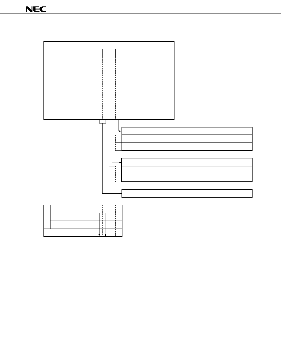
289
�
PD17704, 17705, 17707, 17708, 17709
Figure 19-3. Configuration of BEEP/General-Purpose Port Pin Function Selection Register
Name
Flag symbol
b
3
0
b
2
0
b
1
B
E
E
P
1
S
E
L
b
0
B
E
E
P
0
S
E
L
Address
13H
Read/Write
R/W
BEEP/general-purpose port
pin function selection
Power-ON reset
WDT&SP reset
CE reset
Clock stop
At reset
0
0
0
0
0
0
0
0
0
0
0
1
Uses P1D0/BEEP0 pin as general-purpose I/O port
Uses P1D0/BEEP0 pin for BEEP
Selects general-purpose I/O port or BEEP
Uses P1D1/BEEP1 pin as general-purpose I/O port
Uses P1D1/BEEP1 pin for BEEP
Selects general-purpose I/O port or BEEP
Fixed to 0
0
1
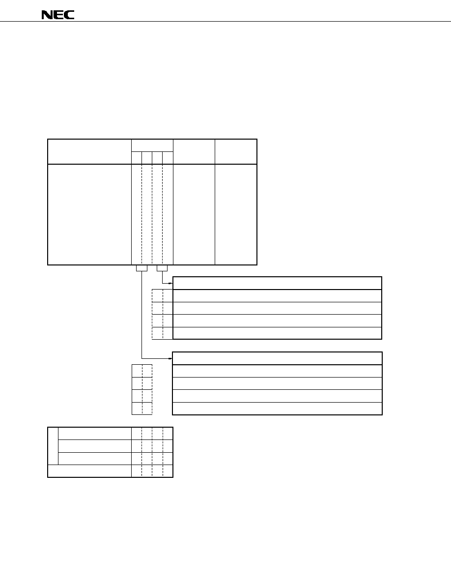
290
�
PD17704, 17705, 17707, 17708, 17709
19.3 Clock Selection Block and Clock Generation Block
The clock selection block selects the output frequency of BEEP1 and BEEP0 by using the BEEP clock selection
register.
The clock generation block generates the clock to be output to BEEP0 and BEEP1.
The clock frequency generated is 1 kHz, 3 kHz, 4 kHz, 6.7 kHz, 67 Hz, or 200 Hz.
Figure 19-4. Configuration of BEEP Clock Selection Register
Name
Flag symbol
b
3
B
E
E
P
1
C
K
1
b
2
B
E
E
P
1
C
K
0
b
1
B
E
E
P
0
C
K
1
b
0
B
E
E
P
0
C
K
0
Address
14H
Read/Write
R/W
BEEP clock selection
Power-ON reset
WDT&SP reset
CE reset
Clock stop
At reset
0
0
0
0
0
0
0
0
0
0
0
0
0
0
0
0
0
1
0
1
1 kHz
3 kHz
4 kHz
6.7 kHz
Sets output frequency of BEEP0
4 kHz
3 kHz
200 Hz
67 Hz
Sets output frequency of BEEP1
0
0
1
1
0
1
0
1
0
0
1
1

291
�
PD17704, 17705, 17707, 17708, 17709
19.4 Output Waveform of BEEP
The duty factor of the BEEP output waveform is 50%.
Example
f = 3 kHz
f = 1 kHz
f = 200 Hz
f: output frequency of BEEP
166.7 s 166.7 s
500 s
2.5 ms
2.5 ms
500 s
�
�
�
�
19.5 Status at Reset
19.5.1 At power-ON reset
The P1D0/BEEP0 and P1D1/BEEP1 pins are set in the general-purpose input port mode.
19.5.2 At WDT&SP reset
The P1D0/BEEP0 and P1D1/BEEP1 pins are set in the general-purpose input port mode.
19.5.3 On execution of clock stop instruction
The P1D0/BEEP0 and P1D1/BEEP1 pins are set in the general-purpose I/O port mode, and retain the previous
input or output status.
19.5.4 At CE reset
The P1D0/BEEP0 and P1D1/BEEP1 pins are set in the general-purpose I/O port mode, and retain the previous
input or output status.
19.5.5 In halt status
The previous status is retained.
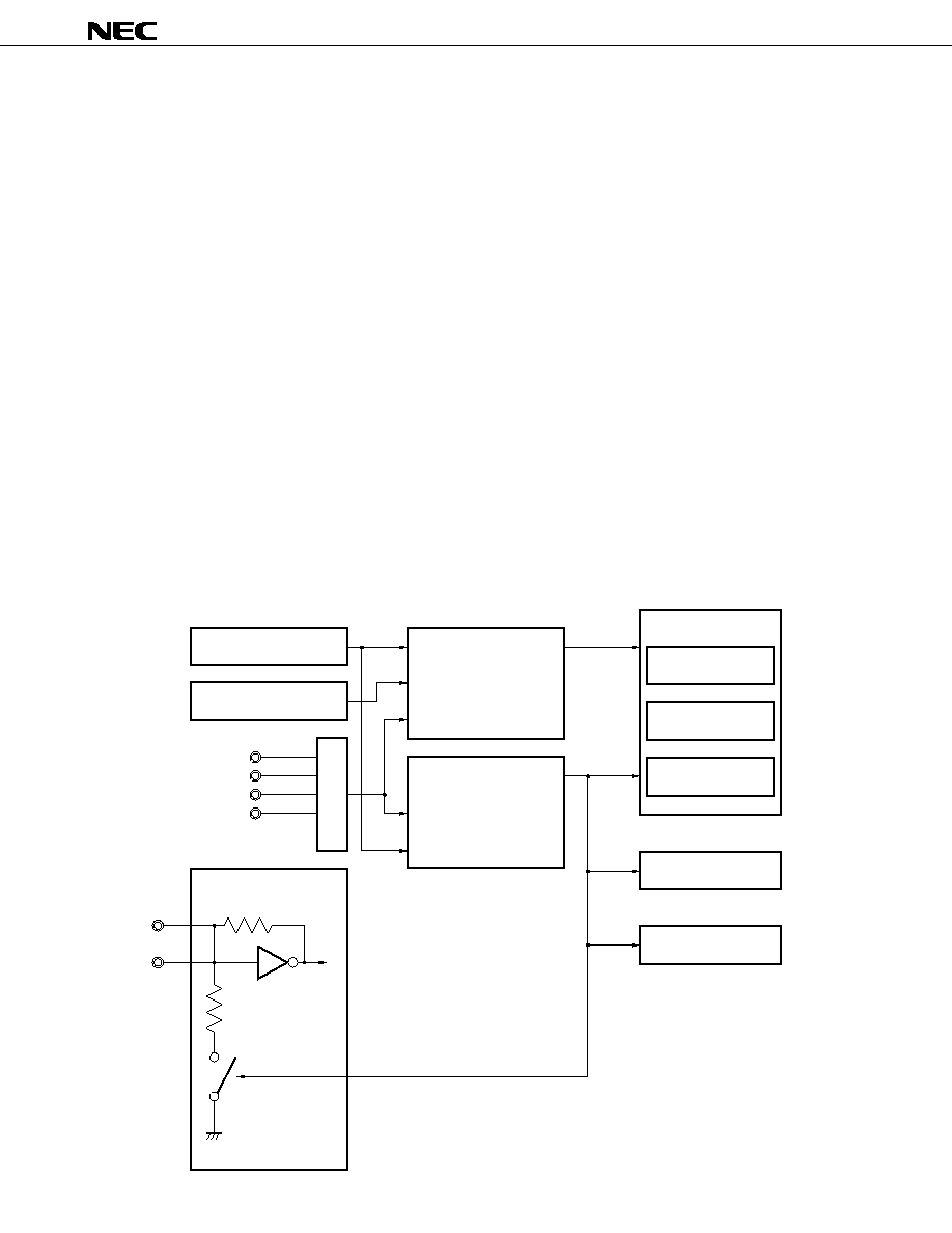
292
�
PD17704, 17705, 17707, 17708, 17709
20. STANDBY
The standby function is used to reduce the current consumption of the device while the device is backed up.
20.1 Outline of Standby Function
Figure 20-1 outlines the standby block.
The standby function reduces the current consumption of the device by partly or totally stopping the device
operation.
The following three types of standby functions are available for selection as the application requires.
�
Halt function
�
Clock stop function
�
Device operation control function by CE pin
The halt function reduces the current consumption of the device by stopping the CPU operation by using a dedicated
instruction "HALT h".
The clock stop function reduces the current consumption of the device by stopping the oscillation of the oscillation
circuit by using a dedicated instruction "STOP s".
The CE pin can be said to be one of the standby functions because it can be used to control the operation of the
PLL frequency synthesizer and to reset the device.
Figure 20-1. Outline of Standby Block
Interrupt control block
BTM0CY
P0D3/AD3
P0D2/AD2
P0D1/AD1
P0D0/AD0
Input latch
Oscillation circuit
X
OUT
X
IN
Halt control circuit
HALT h
Clock stop
control circuit
STOP s
CPU
Program counter
ALU
System register
Control register
Instruction decoder
293
�
PD17704, 17705, 17707, 17708, 17709
20.2 Halt Function
20.2.1 Outline of halt function
The halt function stops the operating clock of the CPU by executing the "HALT h" instruction.
When this instruction is executed, the program is stopped until the halt status is later released. Therefore, the
current consumption of the device in the halt status is reduced by the operating current of the CPU.
The halt status is released by using basic timer 0 carry FF, interrupt, or port input (P0D).
The release condition is specified by operand "h" of the "HALT h" instruction.
20.2.2 Halt status
In the halt status, all the operations of the CPU are stopped. In other words, execution of the program is stopped
at the "HALT h" instruction. However, the peripheral hardware units continue the operation specified before execution
of the "HALT h" instruction.
For the operation of each peripheral hardware unit, refer to 20.4 Device Operation in Halt and Clock Stop Status.
20.2.3 Halt release condition
Figure 20-2 shows the halt release condition.
The halt release condition is specified by 4-bit data specified by operand "h" of the "HALT h" instruction.
The halt status is released when the condition specified by "1" in operand "h".
When the halt status is released, program execution is started from the instruction after the "HALT h" instruction.
If the halt status is released by an interrupt, the operation to be performed after the halt status has been released
differs depending on whether the interrupts are enabled (EI status) or disabled (DI status) when an interrupt source
(IRQxxx = 1) is issued with the interrupt (IPxxx = 1) enabled.
If two or more releasing conditions are specified, the halt status is released when one of the specified condition
is satisfied.
If 0000B is set as halt release condition "h", no releasing condition is set. If the device is reset (by means of power-
ON reset, WDT&SP reset, or CE reset) at this time, the halt status is released.
Figure 20-2. Halt Release Condition
Operand
HALT h (4 bits)
b
3
b
2
b
1
b
0
0
1
Released when high level is input to port 0D
Released when basic timer 0 carry FF is set to 1
Undefined (Fix this bit to "0".)
Released when interrupt is accepted
Not released even if condition is satisfied
Released if condition is satisfied
Sets halt status releasing condition
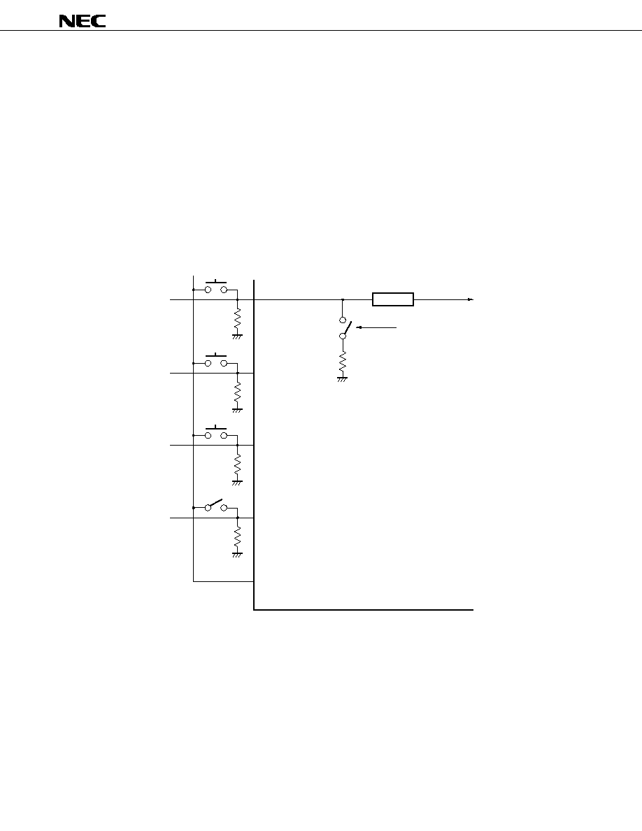
294
�
PD17704, 17705, 17707, 17708, 17709
20.2.4 Releasing halt by input port (P0D)
The halt releasing condition using an input port is specified by the "HALT 0001B" instruction.
When the halt releasing condition using an input port is specified, the halt status is released if a high level is input
to one of the P0D0 through P0D3 pins.
The P0D0 through P0D3 pins are multiplexed with the A/D converter input pins AD0 through AD3, and the halt status
is not released when these pins are used as A/D converter input pins.
An example is given below.
�
To use as key matrix
The P0D0 through P0D3 pins are general-purpose input port pins which can be set in the input or output mode
in 1-bit units and can be connected to an internal pull-down resistor. If connection of the internal pull-down
resistor is specified by software, an external resistor can be eliminated as shown in this example (the internal-
pull down resistor is connected at power-ON reset).
The "HALT 0001B" instruction is executed after the general-purpose output ports for key source signal are made
high. Note that if an alternate switch is used as shown by switch A in the above figure, the halt status is released
immediately because a high level is input to the P0D0/AD0 pin while switch A is closed.
P0D3/AD3
P0DPLD3 flag
P0D2/AD2
P0D1/AD1
P0D0/AD0
Switch A
General-purpose output port
Latch

295
�
PD17704, 17705, 17707, 17708, 17709
20.2.5 Releasing halt status by basic timer 0 carry FF
Releasing the halt status by using the basic timer 0 carry FF is specified by the "HALT 0010B" instruction.
When releasing the halt status by the basic timer 0 carry FF is specified, the halt status is released as soon as
the basic timer 0 carry FF has been set to 1.
The basic timer 0 carry FF corresponds to the BTM0CY flag on a one-to-one basis and is set at fixed time intervals
(100, 50, 20, or 10 ms). Therefore, the halt status can be released at fixed time intervals.
Example To release halt status every 100 ms to execute processing A
HLTTMR
DAT
0010B
; Symbol definition
INITFLG
NOT BTM0CK1, NOT BTM0CK0 ; Sets time interval of basic timer 0 to 100 ms
LOOP:
HALT
HLTTMR
; Specifies setting of basic timer 0 carry FF as halt releasing condition
SKT1
BTMOCY
; Embedded macro
BR
LOOP
; Branches to LOOP if BTM0CY flag is not set
Processing A
; Executes processing A if carry occurs
BR
LOOP
20.2.6 Releasing halt status by interrupt
Releasing the halt status by an interrupt is specified by the "HALT 1000B" instruction.
When releasing the halt status by an interrupt is specified, the halt status is released as soon as the interrupt has
been accepted.
Many interrupt sources are available as described in 12. INTERRUPTS. Which interrupt source is used to release
the halt status must be specified in advance in software.
To accept an interrupt, each interrupt request must be issued from each interrupt source and each interrupt must
be enabled (by setting the corresponding interrupt enable flag).
Therefore, the interrupt is not accepted even if the interrupt request is issued, and the halt status is not released.
When the halt status is released by accepting an interrupt, the program flow branches to the vector address of the
interrupt.
When the RETI instruction is executed after interrupt servicing, the program flow is restored to the instruction after
the HALT instruction.
If all the interrupts are disabled (DI status), the halt status is released by enabling an interrupt (IPxxx = 1) and issuing
an interrupt source (IRQxxx = 1), and the flow of the program goes to the instruction after the HALT instruction.

296
�
PD17704, 17705, 17707, 17708, 17709
Example Releasing halt status by timer 0 and INT0 pin interrupts
In this example, the halt status is released and processing B is executed when timer 0 interrupt is
accepted. And processing A is executed when INT0 pin interrupt is accepted.
Each time the halt status has been released, processing C is executed.
HLTINT
DAT
1000B
; Symbol definition
START:
; Address 0000H
BR
MAIN
;*** Interrupt vector address ***
NOP
; SI01
NOP
; SI00
NOP
; TIMER3
NOP
; TIMER2
NOP
; TIMER1
BR
INTTM0
; Branches to timer 0 interrupt processing
NOP
; INT4
NOP
; INT3
NOP
; INT2
NOP
; INT1
BR
INT0
; Branches to INT0 interrupt processing
NOP
; CE DOWN EDGE
INT0:
; INT0 pin interrupt vector address (000BH)
Processing A
; INT0 pin interrupt processing
EI
RETI
INTMM0:
Processing B
; Timer 0 interrupt processing
EI
RETI
MAIN:
INITFLG
NOT TMOCK1, TM0CK0
; Sets timer 0 count clock to 100
�
s
MOV
DBF1, #0
MOV
DBF0, #0AH
PUT
TM0M,DBF
; Sets time interval of timer 0 interrupt to 1 ms
SET2
TM0RES, TM0EN
; Resets and starts timer 0
SET2
IPTM0, IP0
; Enables INT0 and timer 0 interrupts
LOOP:
Processing C
; Main routine processing
EI
; Enables all interrupts
HALT
HLTINT
; Specifies releasing halt status by interrupt
;<1>
BR
LOOP
If the INT0 pin interrupt request and timer 0 interrupt request are issued simultaneously in the halt status,
processing A for the INT0 pin, which has the higher hardware priority, is executed.
After execution of processing A and when "RETI" is executed, the program branches to the "BR LOOP"
instruction of <1>. However, the "BR LOOP" instruction is not executed, and timer 0 interrupt is immediately
accepted.
When the "RETI" instruction is executed after processing B of timer 0 interrupt has been executed, the
"BR LOOP" instruction is executed.

297
�
PD17704, 17705, 17707, 17708, 17709
Caution To reset the interrupt request flag (IRQxxx) once before the halt instruction is executed, insert
a NOP instruction (or one or more other instructions) between the HALT instruction and the
instruction that resets the interrupt request flag (IRQxxx) as shown below. If a NOP instruction
(or one or more other instructions) is not inserted, the interrupt request flag is not reset, and
therefore, the halt status is released immediately.
Example
:
:
; IRQxxx is set at certain timing
:
CLR1
IRQ
���
; Resets IRQxxx flag once
NOP
; Resets IRQxxx flag at this timing
; Unless this period is missing, the IRQxxx flag is not reset,
; and the next HALT instruction is immediately released
HALT
1000B
;

298
�
PD17704, 17705, 17707, 17708, 17709
20.2.7 If two or more releasing conditions are specified at same time
If two or more halt releasing conditions are specified at same time, the halt status is released when one of the
conditions is satisfied.
The following program example shows how the releasing conditions are identified if two or more conditions are
satisfied at the same time.
Example
HLTINT
DAT
1000B
HLTBTM
DAT
0010B
HLTP0D
DAT
0001B
P0D
MEM
0.73H
START:
BR
MAIN
;*** Interrupt vector address ***
NOP
; SI01
NOP
; SI00
NOP
; TIMER3
NOP
; TIMER2
NOP
; TIMER1
NOP
; TIMER0
NOP
; INT4
NOP
; INT3
NOP
; INT2
NOP
; INT1
BR
INT0
; Branches to INT0 interrupt processing
NOP
; CE DOWN EDGE
INT0:
; INT0 pin interrupt vector address (000BH)
Processing A
; INT0 pin interrupt processing
EI
RETI
BTMOUP:
; Timer carry FF processing
Processing B
RET
P0DP:
; P0D input processing
Processing C
RET
MAIN:
INITFLG NOT BTM0CK1, NOT BTM0CK0
; Selects 100 ms as clock of basic timer 0
SET1
IP0
; Enables INT0 pin interrupt
EI
LOOP:
HALT HLTINT OR HLTBTM OR HLTP0C
; Selects interrupt, timer carry FF, and P0D input as halt releasing conditions
SKF1
BTM0CY
; Detects BTM0CY flag
CALL
BTM0UP
; Timer carry FF processing if flag is set to 1
SKF
P0D, 1111B
; Detects P0D input
CALL
P0DP
; Port input processing if P0D is high
BR
LOOP

299
�
PD17704, 17705, 17707, 17708, 17709
In the above example, three halt status releasing conditions, INT0 pin interrupt, 100-ms basic timer 0 carry FF, and
port 0D input, are specified.
To identify which condition has released the halt status, a vector address (interrupt), BTM0CY flag (timer carry FF),
and port register (port input) are detected.
To use two or more releasing conditions, the following two points must be noted.
�
When the halt status is released, all the specified releasing conditions must be detected.
�
The releasing condition with the higher priority must be detected first.
20.3 Clock Stop Function
20.3.1 Outline of clock stop function
The clock stop function stops the oscillation circuit of a 4.5-MHz crystal resonator by executing the "STOP s"
instruction (clock stop status).
Therefore, the current consumption of the device is reduced to 30
�
A MAX.
20.3.2 Clock stop status
In the clock stop status, all the device operations of the CPU and peripheral hardware units are stopped because
the generation circuit of the crystal resonator is stopped.
For the operations of the CPU and peripheral hardware units, refer to 20.4 Device Operation in Halt and Clock
Stop Status.
In the clock stop status, the power failure detection circuit does not operate even if the supply voltage V
DD
of the
device is raised to 2.2 V. Therefore, the data memory can be backed up at a low voltage. For the power failure detection
circuit, refer to 21. RESET.
20.3.3 Releasing clock stop status
Figure 20-3 shows the stop status releasing conditions.
The stop status releasing condition is specified by 4-bit data specified by operand "s" of the "STOP s" instruction.
The stop status is released when the condition specified by "1" in operand "s" is satisfied.
When the stop status has been released, a halt period which is half the time (t
SET
/2) specified by the basic timer
0 clock selection register as oscillation circuit stabilization wait time has elapsed, and the program execution is started
from the instruction next to the "STOP s" instruction. If releasing the stop status by an interrupt is specified, however,
the program operation after the stop status has been released differs depending on whether the interrupt is enabled
(EI status) or disabled (DI status) when an interrupt source is issued (IRQxxx = 1) with the interrupt enabled (IPxxx
= 1).
If all the interrupts are enabled (EI status), the stop status is released when the interrupt is enabled (IPxxx = 1)
and the interrupt source is issued (IRQxxx = 1), and the program flow returns to the instruction next to the STOP
instruction.
If all the interrupts are disabled (DI status), the stop status is released when the interrupt is enabled (IPxxx = 1)
and the interrupt resource is issued (IRQxxx = 1), and the program flow returns to the instruction next to the STOP
instruction.
If two or more releasing conditions are specified at one time, and if one of the conditions is satisfied, the stop status
is released.
If 0000B is specified as stop releasing condition "s", no releasing condition is satisfied. If the device is reset at
this time (by means of power-ON reset, or CE reset), the stop status is released.
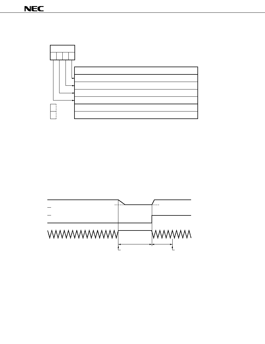
300
�
PD17704, 17705, 17707, 17708, 17709
Figure 20-3. Stop Releasing Conditions
Operand
STOP s (4 bits)
b
3
b
2
b
1
b
0
0
1
Releases when high level is input to port 0D
Undefined (Fix this bit to "0".)
Undefined (Fix this bit to "0".)
Released by interrupt of falling edge of INT0 through INT4 pins and CE pin
Not released even if condition is statisfied
Released if condition is satisfied
Specifies stop status releasing condition
The "STOP s" instruction is executed as a "NOP" instruction when the CE pin rises and when the CE reset counter
operates.
The operating status of the CE reset counter can be detected by the CECNTSTT flag (for the CE reset counter,
refer to 21. RESET).
20.3.4 Releasing clock stop status by high level input of port 0D
Figure 20-4 illustrates how the clock stop status is released by the high level input to port 0D.
Figure 20-4. Releasing Clock Stop Status By High Level Input of Port 0D
V
DD
P0D
X
OUT
5 V
0 V
H
L
2.2 V
STOP s instruction
Starts from instruction next to
STOP s
Oscillation stops
t
SET
/2
HALT period
t
SET
: basic timer 0 setting time
20.3.5 Cautions on releasing clock stop status
For the cautions on releasing the clock stop status, refer to (2) Releasing from clock stop status in 21.4.4
Cautions on raising supply voltage V
DD
.

301
�
PD17704, 17705, 17707, 17708, 17709
20.4 Device Operation in Halt and Clock Stop Status
Table 20-1 shows the operations of the CPU and peripheral hardware units in the halt and clock stop status.
In the halt status, all the peripheral hardware units continue the normal operation until instruction execution is
stopped.
In the clock stop status, all the peripheral hardware units stop operation.
The control registers that control the operations of the peripheral hardware units operate normally (not initialized)
in the halt status, but are initialized to specified values when the clock stop instruction is executed.
In other words, all peripheral hardware continues the operation specified by the control register in the halt status,
and the operation is determined by the initialized value of the control register in the clock stop status.
For the values of the control registers in the clock stop status, refer to 8. REGISTER FILE (RF).
Table 20-1. Device Operation in Halt and Clock Stop Status
Peripheral Hardware
Status
Halt
Clock stop
Program counter
Stops at address of HALT instruction
Stops at address of STOP instruction
System register
Retained
Retained
Peripheral register
Retained
Partly initialized
Note 1
Control register
Retained
Partly initialized
Note 1
Timer
Normal operation
Operation stops
PLL frequency synthesizer
Normal operation
Note 2
Operation stops
A/D converter
Normal operation
Operation stops
D/A converter
Normal operation
Stops operation and used as general-
purpose output port
Serial interface
Stops operation when internal clock (master)
Stops operation and used as general-
is selected and continues operation when
purpose I/O port
external clock (slave) is selected
Frequency counter
Normal operation
Stops operation and used as general-
purpose input port
BEEP output
Normal operation
Stops operation and used as general-
purpose I/O port
General-purpose I/O port
Normal operation
Retained
General-purpose input port
Normal operation
Input port
General-purpose output port
Normal operation
Retains output latch
Notes 1. For the value to which these registers are initialized, refer to 5. SYSTEM REGISTER (SYSREG) and
8. REGISTER FILE (RF).
2. The PLL frequency synthesizer is automatically disabled by the low level input to the CE pin.
20.5 Cautions on Processing of Each Pin in Halt and Clock Stop Status
The halt status is used to reduce the current consumption when, say, only the watch is used.
The clock stop function is used to reduce the current consumption of the device to only use the data memory.
Therefore, the current consumption must be reduced as much as possible in the halt status or clock stop status.
At this time, the current consumption significantly varies depending on the status of each pin, and the points shown
in Table 20-2 must be noted.

302
�
PD17704, 17705, 17707, 17708, 17709
Table 20-2. Status of Each Pin in Halt and Clock Stop Status and Cautions (1/2)
Pin Function
Pin Symbol
Status of Each Pin and Cautions on Processing
Halt status
Clock stop status
General-
Port 0A
P0A3/SDA
purpose
P0A2/SCL
I/O port
P0A1/SCK0
P0A0/SO0
Port 0B
P0B3/SI0
P0B2/SCK1
P0B1/SO1
P0B0/SI1
Port 0C
P0C3-P0C0
Port 1D
P1D3
P1D2
P1D1/BEEP1
P1D0/BEEP0
Port 2A
P2A2
P2A1/FCG1
P2A0/FCG0
Port 2B
P2B3-P2B0
Port 2C
P2C3-P2C0
Port 2D
P2D2-P2D0
Port 3A
P3A3-P3A0
Port 3B
P3B3-P3B0
Port 3C
P3C30P3C0
Port 3D
P3D3-P3D0
General-
Port 0D
P0D3/AD3
purpose
|
input port
P0D0/AD0
Port 1A
P1A3/INT4
P1A2/INT3
P1A1
P1A0/TM0G
Port 1C
P1C3/AD5
P1C2/AD4
P1C1/AMIFC
P1C0/FMIFC
General-
Port 1B
P1B3
purpose
P1B2/PWM2
output port
|
P1B0/PWM0
Retains status before halt
(1) When specified as output pin
Current consumption increases if pin
is externally pulled down while it
outputs high level, or externally pulled
up while it outputs low level.
Exercise care in using N-ch open-
drain output (P0A3, P0A2, P1B3
through P1B0)
(2) When specified as input pin
Current consumption increases due
to noise if pin is floated
(3) Port 0D (P0D3/AD3 through P0D0/
AD0)
Current consumption increases if pin
is externally pulled up because it is
provided with pull-down resistor
selectable by software
(4) Port 1C (P1C3/AD5, P1C2/AD4,
P1C1/AMIFC, P1C0/FMIFC)
When P1C1/AMIFC or P1C0/FMIFC
pin is used for IF counter, current
consumption increases because
internal amplifier operates
All port pins are set in general-purpose
port mode (except P0D3/AD3 through
P0D0/AD0, P1A3/INT4, P1A2/INT3,
P1C3/AD5, and P1C2/AD4)
Input or output mode of general-purpose
I/O port set before clock stop status is
retained.
(1) When specified as general-purpose
output port
Current consumption increases due
to noise if pin is floated
(2) When specified as general-purpose
input port
Current consumption does not
increase due to noise even if pin is
floated
(3) P1A3/INT4, P1A2/INT3
Set as interrupt pin and current
consumption increases due to external
noise if pin is floated
(4) P0D3/AD3 through P0D0/AD0,
P1C3/AD5, P1C2/AD4
Pin used for A/D converter is retained
as is.
Pull-down resistor of P0D3 through
P0D0 pin retains previous status
Specified as general-purpose output port.
Output contents are retained as is. If pin
is externally pulled down while it outputs
high level or externally pulled up while it
outputs low level, current consumption
increases

303
�
PD17704, 17705, 17707, 17708, 17709
Table 20-2. Status of Each Pin in Halt and Clock Stop Status and Cautions (2/2)
Pin Function
Pin Symbol
Status of Each Pin and Cautions on Processing
Halt status
Clock stop status
External interrupt
INT4-INT0
Current consumption increases due to noise if pin is floated
PLL frequency
VCOL
synthesizer
VCOH
EO0
EO1
Crystal oscillation
X
IN
circuit
X
OUT
20.6 Device Operation Control Function of CE Pin
The CE pin controls the following functions by the input level and rising edge of the signal input from an external
source.
�
PLL frequency synthesizer
�
Interrupt by falling edge of CE pin
�
Resetting of device
20.6.1 Controlling operation of PLL frequency synthesizer
The PLL frequency synthesizer can operate only when the CE pin is high.
It is automatically disabled when the CE pin is low.
When the synthesizer is disabled, the VCOH and VCOL pins are internally pulled down, and the EO0 and EO1
pins are floated. For details, refer to 17.5 PLL Disabled Status.
The PLL frequency synthesizer can be disabled in software even when the CE pin is high.
20.6.2 Controlling interrupt by falling edge input of CE pin
An interrupt can be generated by the falling edge of the CE pin. For details, refer to 12. INTERRUPTS.
Current consumption increases during PLL
operation.
When PLL is disabled, pin is in following
status:
VCOH, VCOL : internally pulled down
EO1, EO0
: floated
PLL is automatically disabled if CE pin
goes low
PLL is disabled
VCOH, VCOL : internally pulled down
EO1, EO0
: floated
Current consumption changes due to
oscillation waveform of crystal oscillation
circuit.
The higher oscillation amplitude, the lower
current consumption.
Oscillation amplitude must be evaluated
because it is influenced by crystal resonator
or load capacitor used
X
IN
pin is internally pulled down, and X
OUT
pin outputs high level

304
�
PD17704, 17705, 17707, 17708, 17709
20.6.3 Resetting device
The device can be reset (CE reset) by raising the CE pin.
The device can also be reset as follows:
�
Power-ON reset on application of supply voltage V
DD
�
Watchdog timer reset for software hang-up detection and stack overflow/underflow reset
�
Reset by RESET pin
For details, refer to 21. RESET.
20.6.4 Signal input to CE pin
The CE pin does not accept a low level or high level of less than 167
�
s to prevent malfunctioning due to noise.
The level of the signal input to the CE pin can be detected by the CE pin status detection flag of the CE pin interrupt
request register (RF address 3FH).
Figure 20-5 shows the relationship between the input signal and CE flag.
Figure 20-5. Relationship between Input Signal of CE Pin and CE Flag
CE pin
CE flag
H
L
1
0
Less than 167
s
167
s
PLL can operate
PLL disabled
PLL disabled
Note
CE reset is effected in
synchronization with next
basic timer 0 carry FF
(When CE reset count
register is "1")
Less than 167
s
167
s
CE reset
�
�
�
�
Note
Unless the PLL mode selection register and PLL reference frequency selection register are rewritten by
software, the PLL disabled status is retained.

305
�
PD17704, 17705, 17707, 17708, 17709
20.6.5 Configuration and function of CE pin interrupt request register
The CE pin interrupt request register detects the input signal level of the CE pin.
Figure 20-6 shows the configuration of the CE pin interrupt request register.
Figure 20-6. Configuration of CE Pin Interrupt Request Register
Name
Flag symbol
b
3
C
E
b
2
0
b
1
C
E
C
N
T
S
T
T
b
0
I
R
Q
C
E
Address
3FH
Read/Write
R
Note
CE pin interrupt request
Power-ON reset
WDT&SP reset
CE reset
Clock stop
At Reset
U
U
U
U
0
0
0
0
0
0
0
R
R
0
1
No interrupt request
Interrupt request
Sets interrupt request issuance status of CE pin
Stops
Operates
Detects status of CE reset counter
Low level is input
High level is input
Detects status of CE pin
Fixed to
"
0
"
0
1
0
1
U: Undefined R: Retained
Note
IRQCE is a R/W flag.

306
�
PD17704, 17705, 17707, 17708, 17709
21. RESET
21.1 Outline of Reset
The reset function is used to initialize the device.
The
�
PD17709 can be reset in the following ways:
�
CE reset
�
Power-ON reset
�
Reset by RESET pin
�
WDT&SP reset
Figure 21-1. Configuration of Reset Block
X
OUT
X
IN
V
DD
RESET
CE
STOP s
instruction
Voltage
detection
circuit
Falling
detection
circuit
Rising
detection
circuit
BTM0CY flag read
Power failure detection block
Timer FF block
Divider
Selector
Basic timer 0
carry
R
S
Q
Basic timer 0
carry disable FF
Power-ON clear signal (POC)
Reset
control
circuit
STOP instruction
CE reset timer
carry counter
Watchdog timer stack
overflow/underflow
detection block
CE reset signal
WDT&SP reset signal
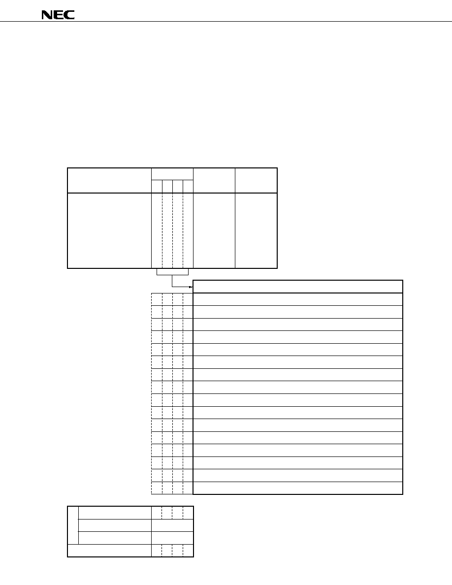
307
�
PD17704, 17705, 17707, 17708, 17709
21.2 CE Reset
CE reset is effected by raising the CE pin.
When the CE pin goes high, the next rising edge of the basic timer 0 carry FF setting pulse is counted. When the
count value coincides with the value set to the CE reset timer carry counter register (1 to 15 counts), the reset signal
is generated.
When CE reset is effected, the program counter, stack, system registers, and some of the control registers are
initialized to the initial values, and program execution is started from address 0000H. For the initial value of each
register, refer to the description of each register.
Figure 21-2. Configuration of CE Reset Timer Carry Counter Register
Name
Flag symbol
b
3
C
E
C
N
T
3
b
2
C
E
C
N
T
2
b
1
C
E
C
N
T
1
b
0
C
E
C
N
T
0
Address
06H
Read/Write
R/W
CE reset timer carry counter
Power-ON reset
WDT&SP reset
CE reset
Clock stop
At reset
0
0
0
0
0
0
0
0
1
1
1
1
1
1
1
1
0
0
0
1
0
1
0
1
0
1
0
1
0
1
0
1
0
1
1
1
Setting prohibited
1 count
2 counts
3 counts
4 counts
5 counts
6 counts
7 counts
8 counts
9 counts
10 counts
11 counts
12 counts
13 counts
14 counts
15 counts
Sets number of counts of timer carry counter for CE reset
0
0
0
0
1
1
1
1
0
0
0
0
1
1
1
1
0
0
0
0
1
1
0
0
1
1
0
0
1
1
0
0
1
1
0
0
Retained
Retained
308
�
PD17704, 17705, 17707, 17708, 17709
The operation of CE reset differs depending on whether the clock stop instruction is used or not.
This difference is described in 21.2.1 and 21.2.2 below.
21.2.3 describes the points to be noted when CE reset is effected.
21.2.1 CE reset without clock stop (STOP s) instruction
Figure 21-2 shows the operation.
When the CE pin has gone high, the CE reset timer carry counter starts counting at the rising edge of the basic
timer 0 carry FF setting pulse.
Figure 21-3. CE Reset Operation without Clock Stop Instruction (1/2)
(a) Normal operation
�
When "N" is set to CE reset timer carry counter
�
When "1" is set to CE reset timer carry counter
V
DD
CE
X
OUT
BTM0CY flag
setting pulse
CE reset timer
carry counter
Set value of CE reset timer
carry counter
CE reset signal
5 V
0 V
H
L
H
L
H
L
H
L
H
H
L
L
t
SET
0
1
2
3
N�2
N�1
N
0
N
CE reset
V
DD
CE
X
OUT
BTM0CY flag
setting pulse
CE reset timer
carry counter
Set value of CE reset
timer carry counter
CE reset signal
CE reset
5 V
0 V
H
L
H
L
H
L
H
L
H
H
L
L
t
SET
0
1
0
1
309
�
PD17704, 17705, 17707, 17708, 17709
Figure 21-3. CE Reset Operation without Clock Stop Instruction (2/2)
(b) If status of CE pin changes while CE counter operates
At this time, the CE reset timer carry counter status is not affected.
21.2.2 CE reset with clock stop (STOP s) instruction used
Figure 21-4 shows the operation.
When the clock stop instruction is used, the clock stop signal is output when the "STOP s" instruction is executed,
and oscillation is stopped and the device operation is stopped.
When the CE pin goes high, the clock stop status is released, and oscillation is started (high level input of P0D
or INT pin interrupt can also be used as the clock stop status releasing conditions. For details, refer to 20. STANDBY).
If the basic timer 0 carry FF setting pulse goes high after the CE pin has gone high, the halt status is released,
and program execution is started from address 0 (CE reset).
As the set time (t
SET
) of the basic timer 0 carry FF setting pulse, the value immediately before the clock stop
instruction is executed is retained.
Because the set value of the CE reset timer carry counter is initialized to 1, CE reset is effected t
SET
/2 after the
CE pin has gone high.
V
DD
CE
X
OUT
BTM0CY flag
setting pulse
CE reset timer
carry counter
Set value of CE reset
timer carry counter
CE reset signal
5 V
0 V
H
L
H
L
H
L
H
L
H
H
L
L
t
SET
0
1
2
3
N�2
N�1
N
0
N
CE reset

310
�
PD17704, 17705, 17707, 17708, 17709
Figure 21-4. CE Reset Operation with Clock Stop Instruction
21.2.3 Cautions on CE reset
Because CE reset is effected regardless of the instruction under execution, the following points (1) and (2) must
be noted.
(1) Time to execute timer processing such as watch
When creating a watch program by using the basic timer 0 carry, the processing time of the program must be
kept to within a specific time.
For details, refer to 13.2.6 Cautions on using basic timer 0.
(2) Processing of data and flags used in program
Exercise care in rewriting the data and flags whose contents must not be changed even when CE reset is
effected, such as security code.
An example is shown below.
V
DD
CE
X
OUT
BTM0CY flag
setting pulse
CE reset timer
carry counter
Set value of CE reset
timer carry counter
Normal operation
5 V
0 V
H
L
H
L
H
L
H
L
H
H
L
L
t
SET
N
1
1
0
Clock stop status
Halt
status
t
SET
/2
STOP s instruction
Clock stop
status
released.
Oscillation
starts
CE reset
Program execution starts from address 0
CE reset signal

311
�
PD17704, 17705, 17707, 17708, 17709
Example 1.
R1
MEM
0.01H
; 1st digit of key input data of security code
R2
MEM
0.02H
; 2nd digit of key input data of security code
R3
MEM
0.03H
; 1st digit data when security code is changed
R4
MEM
0.04H
; 2nd digit data when security code is changed
M1
MEM
0.11H
; 1st digit of current security code
M2
MEM
0.12H
; 2nd digit of current security code
START:
Key input processing
R1
contents of key A
; Security code input wait mode
R2
contents of key B
; Substitutes contents of pressed key to R1 and R2
SET2
CMP, Z
; <1> ; Compares security code and input data
SUB
R1, M1
SUB
R2, M2
SKT1
Z
BR
ERROR
; Input data differs from security code
MAIN:
Key input processing
R3
contents of key C
; Security code rewriting mode
R4
contents of key D
; Substitutes contents of pressed key to R3 and R4
ST
M1, R3
; <2> ; Rewrites security code
ST
M2, R4
; <3>
BR
MAIN
ERROR:
Must not operate
Suppose the security code is "12H" in the program in Example 1. The contents of data memory addresses M1
and M2 are "1H" and "2H", respectively.
If CE reset is effected, the contents of key input and security code "12H" are compared in <1>. If the two are the
same, the normal processing is performed.
If the security code is changed in the main processing, the new code is written to M1 and M2 in <2> and <3>.
Suppose the security code is changed to "34H". Then "3H" and "4H" are written to M1 and M2 in <2> and <3>.
If CE reset is effected as soon as <2> has been executed, program execution is started from address 0000H, without
<3> being executed.
Consequently, the security code is set to "32H", making it impossible to clear the security system.
In this case, create the program shown in Example 2.

312
�
PD17704, 17705, 17707, 17708, 17709
Example 2.
R1
MEM
0.01H
; 1st digit of key input data of security code
R2
MEM
0.02H
; 2nd digit of key input data of security code
R3
MEM
0.03H
; 1st digit data when security code is changed
R4
MEM
0.04H
; 2nd digit data when security code is changed
M1
MEM
0.11H
; 1st digit of current security code
M2
MEM
0.12H
; 2nd digit of current security code
CHANGE
FLG
0.13H.0
; "1" while security code is changed
START:
Key input processing
R1
contents of key A
; Security code input wait mode
R2
contents of key B
; Substitutes contents of pressed key to R1 and R2
SKT1
CHANGE
; <4> ; If CHANGE flag is "1"
BR
SECURITY_CHK
ST
M1, R3
; Rewrites M1 and M2
ST
M2, R4
CLR1
CHANGE
SECURITY_CHK:
SET2
CMP, Z
; <1> ; Compares security code and input data
SUB
R1, M1
SUB
R2, M2
SKT1
Z
BR
ERROR
; Input data differs from security code
MAIN:
Key input processing
R3
contents of key C
; Security code rewriting mode
R4
contents of key D
; Substitutes contents of pressed key to R3 and R4
SET1
CHANGE
; <5> ; Until security code is changed,
; Sets CHANGE flag to "1"
ST
M1, R3
; <2> ; Rewrites security code
ST
M2, R4
; <3>
CLR1
CHANGE
; If security code has been changed,
; Sets CHANGE flag to "0"
BR
MAIN
ERROR:
Must not operate
The program in Example 2 sets the CHANGE flag to "1" in <5> before the security code is rewritten in <2> and
<3>.
Therefore, even if CE reset is effected before <3> is executed, the security code is rewritten in <4>.

313
�
PD17704, 17705, 17707, 17708, 17709
21.3 Power-ON Reset
Power-ON reset is effected by raising the supply voltage V
DD
of the device from a specific level (called a power-
ON clear voltage).
If supply voltage V
DD
is lower than the power-ON clear voltage, a power-ON clear signal (POC) is output from the
voltage detection circuit shown in Figure 21-1.
When the power-ON clear signal is input to the reset control circuit, the crystal oscillation circuit is stopped and
consequently, the device operation is stopped.
At this time, the program counter, stack, system registers, and control registers are initialized (for the initial value,
refer to the description of each register).
If supply voltage V
DD
exceeds the power-ON clear voltage, the power-ON clear signal is deasserted, crystal
oscillation is started, and the device waits for release of the halt status by the basic timer 0 carry which has been
initialized to 100 ms. Program execution is started from address 0 at the rising edge of the basic timer 0 carry FF
setting signal 50 ms after the supply voltage has exceeded the power-ON clear voltage.
Normally, the power-ON clear voltage is 3.5 V, but it is 2.2 V in the clock stop status.
The operations of power-ON reset are described in 21.3.1 and 21.3.2.
The operation when supply voltage V
DD
is raised from 0 V is described in 21.3.3.
Caution Although it is stated that the normal power-ON clear voltage is 3.5 V (MAX.) and that in the clock
stop status is 2.2 V (MAX.), the actual power-ON clear voltage does not exceed these maximum
values.
Figure 21-5. Operation of Power-ON Reset
V
DD
CE
Power-ON clear signal
X
OUT
BTM0CY flag
setting pulse
5 V
0 V
H
L
H
L
H
H
L
L
Power-ON
clear voltage
Power-ON clear released
Oscillation starts
Program starts from
address 0
50 ms
Halt status
Device operation stops
Normal operation

314
�
PD17704, 17705, 17707, 17708, 17709
21.3.1 Power-ON reset during normal operation
Figure 21-6 (a) shows the operation.
As shown, the power-ON clear signal is output and the device operation is stopped if the supply voltage V
DD
drops
below 3.5 V, regardless of the input level of the CE pin.
If V
DD
rises beyond 3.5 V again, program execution starts from address 0000H after a halt of 50 ms.
Normal operation means operation without the clock stop instruction, and includes the halt status set by the halt
instruction.
21.3.2 Power-ON reset in clock stop status
Figure 21-6 (b) shows the operation.
As shown, the power-ON clear signal is output and the device operation is stopped when supply voltage V
DD
drops
below 2.2 V.
However, it does not appear that device operation has changed because the device is in the clock stop status.
If V
DD
rises beyond 3.5 V, program execution starts from address 0000H after a halt of 50 ms.
21.3.3 Power-ON reset when supply voltage V
DD
rises from 0 V
Figure 21-6 (c) shows the operation.
As shown, the power-ON clear signal is output until supply voltage V
DD
rises from 0 V to 3.5 V.
When V
DD
exceeds the power-ON clear voltage, the crystal oscillation circuit starts operating, and program execution
starts from address 0000H after a half of 50 ms.
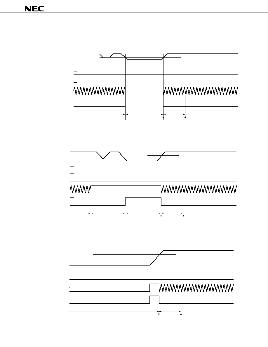
315
�
PD17704, 17705, 17707, 17708, 17709
Figure 21-6. Power-ON Reset and Supply Voltage V
DD
(a) Normal operation (including halt status)
V
DD
CE
Power-ON
clear signal
X
OUT
5 V
3.5 V
0 V
H
L
H
L
H
L
Power-ON clear voltage
Normal operation
Device operation stops
Halt status
50 ms
Power-ON clear released
Oscillation starts
Program starts from address 0
(c) If supply voltage V
DD
rises from 0 V
V
DD
CE
Power ON
clear signal
X
OUT
5 V
3.5 V
2.2 V
0 V
H
L
H
L
H
L
Power-ON clear voltage
Normal operation
STOP s instruction
Clock stop
Device operation stops
Halt status
50 ms
Power-ON clear released
Oscillation starts
Program starts from address 0
(b) In clock stop status
V
DD
CE
Power-ON
clear signal
X
OUT
5 V
3.5 V
0 V
H
L
H
L
H
L
Power-ON clear voltage
Device operation stops
Halt status
50 ms
Power-ON clear released
Oscillation starts
Program starts from address 0

316
�
PD17704, 17705, 17707, 17708, 17709
21.4 Relationship between CE Reset and Power-ON Reset
On the first application of supply voltage V
DD
, power-ON reset and CE reset are performed at the same time.
The reset operations at this time are described in 21.4.1 through 21.4.3.
21.4.4 describes the points to be noted when raising supply voltage V
DD
.
21.4.1 If V
DD
pin and CE pin go high at the same time
Figure 21-7 (a) shows the operation.
At this time, the program starts from address 0000H because of power-ON reset.
21.4.2 If CE pin rises in forced halt status set by power-ON reset
Figure 21-7 (b) shows the operation.
At this time, the program starts from address 0000H because of power-ON reset, in the same manner as 21.4.1.
21.4.3 If CE pin rises after power-ON reset
Figure 21-7 (c) shows the operation.
At this time, the program starts from address 0000H because of power-ON reset, and the program starts from
address 0000H again at the rising edge of the next basic timer 0 carry FF setting signal because of CE reset.
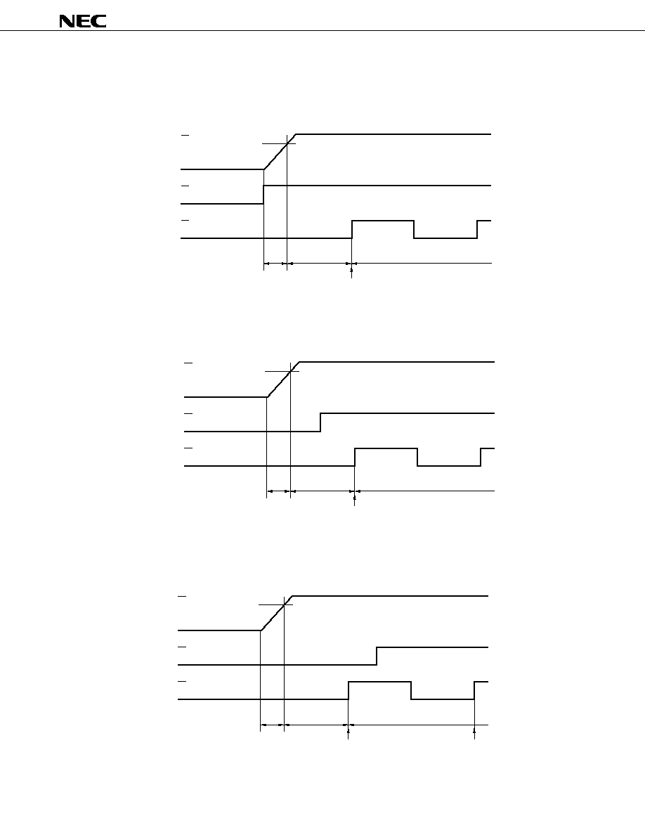
317
�
PD17704, 17705, 17707, 17708, 17709
Figure 21-7. Relationship between Power-ON Reset and CE Reset
(a) When V
DD
and CE pin rise at the same time
(b) If CE pin rises in halt status
(c) If CE pin rises after power-ON reset
V
DD
CE
BTM0CY flag
setting pulse
5 V
3.5 V
0 V
H
L
H
L
Power-ON clear voltage
Opera-
tion
stops
Halt status
50 ms
Normal operation
Power-ON reset
Program starts
CE reset
Program starts
(If CE reset timer carry counter is set to "1")
V
DD
CE
BTM0CY flag
setting pulse
5 V
3.5 V
0 V
H
L
H
L
Power-ON clear voltage
Opera-
tion
stops
Halt status
50 ms
Normal operation
Power-ON reset
Program starts
V
DD
CE
BTM0CY flag
setting pulse
5 V
3.5 V
0 V
H
L
H
L
Power-ON clear voltage
Opera-
tion
stops
Halt status
50 ms
Normal operation
Power-ON reset
Program starts

318
�
PD17704, 17705, 17707, 17708, 17709
21.4.4 Cautions on raising supply voltage V
DD
The following points (1) and (2) must be noted when raising supply voltage V
DD
.
(1) To raise supply voltage V
DD
from level lower than power-ON clear voltage
Supply voltage V
DD
must be raised once to a level higher than 3.5 V.
Figure 21-8 illustrates this.
As shown in the figure, if a voltage less than 3.5 V is applied on application of V
DD
in a program that backs
up V
DD
at 2.2 V by using the clock stop instruction, the power-ON clear signal remains output, and the program
is not executed.
At this time, the output ports of the device output undefined values, increasing the current consumption in some
cases.
Consequently, the backup time when the device is backed up by batteries is substantially shortened.
Figure 21-8. Cautions on Raising V
DD
V
DD
BTM0CY flag
setting pulse
X
OUT
5 V
3.5 V
2.2 V
0 V
H
L
H
L
Power-ON
clear signal
H
L
Power-ON
clear voltage
Operation stops
Halt status
50 ms
Because output ports are
undefined during this period,
current consumption may increase.
Power-ON reset
Progarm starts
Opera-
tion
stops
Normal operation
Back up
Initialize during this
period and then
execute clock stop
instruction
STOP s instruction

319
�
PD17704, 17705, 17707, 17708, 17709
(2) Releasing from clock stop status
If the device is released from the backup status when supply voltage V
DD
is backed up at 2.2 V by using the
clock stop status, V
DD
must be raised to 3.5 V or more within t
SET
/2 after the clock stop status has been released
by INT pin interrupt or high level input to port 0D.
As shown in Figure 21-9, the device is released from the clock stop status by means of CE reset. However,
because the power-ON clear voltage is changed to 3.5 V t
SET
/2 after the clock stop status has been released,
power-ON reset is effected unless V
DD
is 3.5 V or higher.
The same applies when V
DD
is raised.
Figure 21-9. Releasing from Clock Stop Status
P0D
BTM0CY flag
setting pulse
X
OUT
5 V
3.5 V
2.2 V
0 V
0 V
H
L
H
L
Power-ON
clear signal
H
L
Power-ON
clear voltage
Backup in clock stop
status
Halt status
t
SET
/2
Power-ON clear voltage changes
to 3.5 V at this point.
Therefore, V
DD
must be 3.5 V
or higher before this point.
Normal operation
Backup
STOP s instruction
H
V
DD
Program starts
Power-ON clear voltage changes
to 2.2 V at this point.
Therefore, V
DD
must be 3.5 V
or higher before this point.
t
SET
: basic timer 0 setting time
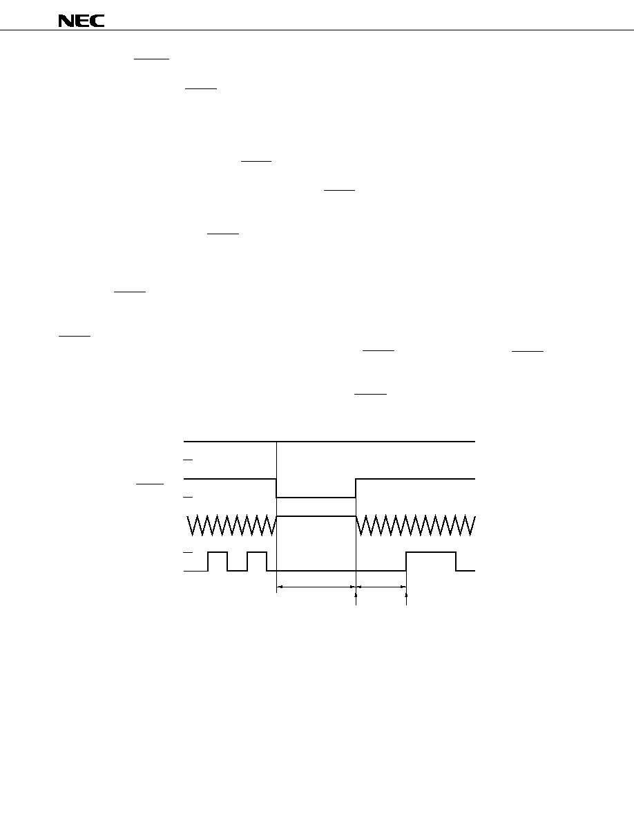
320
�
PD17704, 17705, 17707, 17708, 17709
21.5 Reset by RESET Pin
The device is reset by the RESET pin in the following cases:
�
To reset the device at voltage higher than power-ON clear voltage
�
External reset input in case of software hang-up
Caution If the device is reset by the RESET pin during program execution, the data in the data memory
may be corrupted.
Therefore, be careful when resetting with the RESET pin.
The reset operation is the same as that performed at power-ON reset.
When a low level is input to the RESET pin, an internal reset signal is generated, the crystal oscillation circuit is
stopped, and the device stops operation.
At this point, the program counter, stack, system registers, and control registers are initialized (for the initial value,
refer to the description of each register).
When the RESET pin is raised next time, the crystal oscillation is started, and the device waits to be released from
the halt wait status by the basic timer 0 carry which has been initialized to a 100-ms cycle. The program starts from
address 0 at the rising edge of the basic timer 0 carry FF setting signal 50 ms after a high level has been input to the
RESET pin.
Because the
�
PD17709 has a power-ON reset function, connect the RESET pin to V
DD
via resistor if the RESET
pin is not used for the above application.
Figure 21-10. Reset Operation by RESET Pin
V
DD
RESET
X
OUT
BTM0CY flag
setting pulse
5 V
0 V
H
L
H
L
H
L
Device opeation stops
Halt status
50 ms
Oscillation starts
Program starts
from address 0
321
�
PD17704, 17705, 17707, 17708, 17709
21.6 WDT&SP Reset
WDT&SP reset includes the following:
�
Watchdog timer reset
�
Stack pointer overflow/underflow reset
Figure 21-11. Outline of WDT&SP Reset
21.6.1 Watchdog timer reset
The watchdog timer is a circuit that generates a reset signal when the execution sequence of the program is
abnormal (hung-up).
Hanging-up means that the program jumps to an unexpected routine due to external noise, entering a specific
infinite loop and causing the system to be deadlocked. By using the watchdog timer, the program can be restored
from this hang-up status because a reset signal is generated from the watchdog timer at fixed time intervals and
program execution is started from address 0.
The watchdog timer does not function in the clock stop mode and halt mode.
Resetting by the watchdog timer initializes all the registers except the stack overflow selection register, watchdog
timer counter reset register, basic timer 0 carry register, and CE reset timer carry counter.
The watchdog timer reset is detected by the WDTCY flag (R&Reset).
Instruction
count clock
65536
instruction
counter
131072
instruction
counter
Stack overflow/under
flow reset detection
circuit
WDTRES
ASPRES flag
ISPRES flag
WDTCK1 flag
WDTCK0 falg
WDTCY flag
WDT&SP
reset signal

322
�
PD17704, 17705, 17707, 17708, 17709
21.6.2 Watchdog timer setting flags
These flags can be set only once after power-ON reset on power application or reset by the RESET pin.
The WDTCK0 and WDTCK1 flags select an interval at which the reset signal is output.
The reference time can be selected to the following three conditions:
�
655356 instructions
�
131072 instructions
�
Watchdog timer not set
On power application, 131072 instructions are selected.
If the reset signal generation interval is specified to be 131072 instructions, the watchdog timer FF must be reset
at intervals not exceeding 131072 instructions. The valid reset period is from 1 to 131071 instructions.
If the reset signal generation interval is 65536 instructions, the watchdog timer FF must be reset at intervals not
exceeding 65536 instrutions. The valid reset period is from 1 to 65535 instructions.
Figure 21-12. Configuration of Watchdog Timer Clock Selection Register
Name
Flag symbol
b
3
0
b
2
0
b
1
W
D
T
C
K
1
b
0
W
D
T
C
K
0
Address
02H
Read/Write
R/W
Note
Watchdog timer
clock selection
Power-ON reset
WDT&SP reset
CE reset
Clock stop
At reset
0
0
1
1
0
1
0
1
Does not set watchdog timer
65536 instructions
Setting prohibited
131072 instructions
Selects clock of watchdog timer
Fixed to "0"
0
0
1
1
Retained
Retained
Retained
Note
Can be written only once.

323
�
PD17704, 17705, 17707, 17708, 17709
The WDTRES flag is used to reset the watchdog timer counter.
When this flag is set to 1, the watchdog timer counter is automatically reset.
If the WDTRES flag is set to 1 once within a reference time in which the WDTCK0 and WDTCK1 flags are set, the
reset signal is not output by the watchdog timer.
Figure 21-13. Configuration of Watchdog Timer Counter Reset Register
Name
Flag symbol
b
3
W
D
T
R
E
S
b
2
0
b
1
0
b
0
0
Address
03H
Read/Write
W&Reset
Watchdog timer
counter reset
Power-ON reset
WDT&SP reset
CE reset
Clock stop
At reset
U
U
U
U
0
0
0
0
1
Invalid
Resets watchdog timer counter
Resets watchdog timer counter
Fixed to "0"
U: Undefined

324
�
PD17704, 17705, 17707, 17708, 17709
21.6.3 Stack pointer overflow/underflow reset
A reset signal is generated if the address or interrupt stack overflows or underflows.
Stack pointer overflow/underflow reset can be used to detect a program hang-up in the same manner as watchdog
timer reset.
The reset signal is generated under the following conditions:
� Interrupt due to overflow or underflow of interrupt stack (4 levels)
� Interrupt due to overflow or underflow of address stack (15 levels)
Reset by stack pointer overflow or underflow initializes all the registers, except the stack overflow selection register,
watchdog timer counter reset register, basic timer 0 carry register, and CE reset timer carry counter.
Generation of stack pointer overflow or underflow reset is detected by the WDTCY flag (R&Reset).
21.6.4 Stack pointer setting flag
The stack overflow/underflow reset selection register can be set only once after power-ON reset on power application
or reset by the RESET pin. This register specifies whether reset by address stack overflow or underflow and reset
by interrupt stack overflow or underflow are enabled or disabled.

325
�
PD17704, 17705, 17707, 17708, 17709
Figure 21-14. Configuration of Stack Overflow/Underflow Reset Selection Register
Note
Can be written only once.
Name
Flag symbol
b
3
0
b
2
0
b
1
I
S
P
R
E
S
b
0
A
S
P
R
E
S
Address
05H
Read/Write
R/W
Note
Stack overflow/underflow
reset selection
Power-ON reset
WDT&SP reset
CE reset
Clock stop
At reset
0
0
1
1
0
1
Disables reset
Enables reset
Selects address stack overflow/underflow reset
0
1
Disables reset
Enables reset
Selects interrupt stack overflow/underflow reset
Fixed to "0"
Retained
Retained
Retained

326
�
PD17704, 17705, 17707, 17708, 17709
Figure 21-15. Configuration of WDT&SP Reset Selection Register
Name
Flag symbol
b
3
0
b
2
0
b
1
0
b
0
W
D
T
C
Y
Address
16H
Read/Write
R&Reset
WDT&SP reset
status detection
Power-ON reset
WDT&SP reset
CE reset
Clock stop
At reset
0
0
0
0
1
R
R
0
1
No reset request
Reset request
Detects occurrence of WDT&SP reset
Fixed to "0"
R: Retained

327
�
PD17704, 17705, 17707, 17708, 17709
21.7 Power Failure Detection
Power failure detection is used to identify whether the device has been reset by application of supply voltage V
DD
,
RESET pin, or CE pin.
Because the contents of the data memory and output ports are "undefined" on power application, these contents
are initialized by using power failure detection.
Power failure detection can be performed in two ways: by detecting the BTM0CY flag and the contents of the data
memory (RAM judgment).
21.7.1 and 21.7.2 describe the power failure detection circuit and power failure detection by using the BTM0CY
flag.
21.7.3 and 21.7.4 describe power failure detection by RAM judgment method.
Figure 21-16. Power Failure Detection Flowchart
Program starts
Power failure
detection
Not power failure
Power failure
Initializes data
memory and output
ports
21.7.1 Power failure detection circuit
The power failure detection circuit consists of a voltage detection circuit, and basic timer 0 carry disable flip-flop
that is set by the output (power-ON clear signal) of the voltage detection circuit, and timer carry, as shown in Figure
21-1.
The basic timer 0 carry disable FF is set to 1 by the power-ON clear signal, and is reset to 0 when an instruction
that reads the BTM0CY flag is executed.
When the basic timer 0 carry disable FF is set to 1, the BTM0CY flag is not set to 1.
If the power-ON clear signal is output (at power-ON reset), the program starts with the BTM0CY flag reset. After
that, the BTM0CY flag is disabled from being set until an instruction that reads the flag is executed.
Once the instruction that reads this flag has been executed, the BTM0CY flag is set each time the basic timer 0
carry FF setting pulse rises. Therefore, by detecting the content of the BTM0CY flag when the device is reset, whether
the device has been reset by power-ON reset (power failure) or CE reset (not power failure) can be identified. That
is, the device has been reset by power-ON reset if the BTM0CY flag has been reset to 0. It has been reset by CE
reset if the flag has been set to 1.
Because the voltage at which a power failure can be detected is the same as that at which power-ON reset is
executed, V
DD
= 3.5 V during crystal oscillation and V
DD
= 2.2 V in the clock stop status.
The operation of the BTM0CY flag is the same regardless of whether the device has been reset by the RESET
pin or by power-ON reset.

328
�
PD17704, 17705, 17707, 17708, 17709
21.7.2 Cautions on detecting power failure by BTM0CY flag
The following points must be noted when counting the watch timer by using the BTM0CY flag.
(1) Updating watch
When creating a watch program using the timer carry, the watch must be updated after a power failure has
been detected.
This is because the BTM0CY flag is reset to 0 because it is read after a power failure has been detected. As
a result, counting of the watch is overlooked once.
(2) Watch updating processing time
Updating the watch must be completed before the next basic timer 0 carry FF setting pulse rises.
This is because CE reset is executed before the watch updating processing has been completed if the CE pin
goes high during watch updating processing.
For the details of (1) and (2), refer to (3) Compensating basic timer 0 carry at CE reset in 13.2.6.
The following points must be noted when performing processing in case of a power failure.
(3) Timing to detect power failure
When counting the watch by using the BTM0CY flag, the BTM0CY flag must be read to detect a power failure
before the next basic timer 0 carry FF setting pulse rises after the program has been started from address
0000H.
This is because, if the basic timer 0 carry FF setting time is set to, say, 10 ms, and if the power failure is detected
11 ms after the program has been started, the BTM0CY flag is overlooked once.
For further information, refer to (3) Compensating basic timer 0 carry at CE reset in 13.2.6.
Power failure detection and initial processing must be performed within the time in which the basic timer 0 carry
FF is set, as shown in the example below.
This is because, if the CE pin rises and CE reset is executed during power failure processing or initial processing,
the processing is stopped in midway, causing a problem.
To update the basic timer 0 carry FF setting time in the initial processing, the instruction that changes the setting
time must be executed at the end of the initial processing.
This is because, if the basic timer 0 carry FF setting time is changed before the initial processing, the initial
processing may not be executed to the end because CE reset may be executed.

329
�
PD17704, 17705, 17707, 17708, 17709
Example
START:
; Program address 0000H
; <1>
Processing at reset
; <2>
SKT1
BTM0CY
; Power failure detection
BR
INITIAL
BACKUP:
; <3>
Watch updating
BR
MAIN
INITIAL:
; <4>
Initial processing
; <5>
INITFLG BTM0CK1, BTM0CK0
; Embedded macro
; Sets basic timer 0 carry FF
; Sets time to 10 ms
MAIN:
Main processing
SKT1
BTM0CY
BR
MAIN
Watch updating
BR
MAIN
Operation example (if CE reset timer counter is set to "1")
V
DD
CE
10-ms pluse
50-ms pluse
BTM0CY flag
setting pulse
5 V
0 V
H
L
H
L
50 ms
10 ms
50 ms
<1>
<4>
<1>
<3>
<2>
<2>
Power failure detection
If processing time of <1> + <4> is longer
than 100 ms, CE reset is executed
in the middle of processing <4>.
<5>
CE reset
Power failure detection
If processing time of <1> + <3> is
too long, CE reset is executed.
CE reset
CE reset may be executed immediately depending on when
the basic timer 0 carry FF setting time is changed.
Therefore, if <5> is executed before <4>, power failure
processing <4> may not be executed to the end.

330
�
PD17704, 17705, 17707, 17708, 17709
21.7.3 Power failure detection by RAM judgment method
By the RAM judgment method, a power failure is detected by judging whether the contents of the data memory
at a specific address are a specific value when the device has been reset.
An example of a program that detects a power failure by RAM judgment method is shown below.
By the RAM judgment method, a power failure is detected by comparing an "undefined" value and a "specific" value
because the contents of the data memory are "undefined" on application of supply voltage V
DD
.
Therefore, a power failure may be judged by mistake by this method as described in 21.7.4 Cautions on power
failure detection by RAM judgment method.
Example Program example of power failure detection by RAM judgment method
M012
MEM
0.12H
M034
MEM
0.34H
M056
MEM
0.56H
M107
MEM
1.07H
M128
MEM
1.28H
M16F
MEM
1.6FH
DATA0
DAT
1010B
DATA1
DAT
0101B
DATA2
DAT
0110B
DATA3
DAT
1001B
DATA4
DAT
1100B
DATA5
DAT
0011B
START:
SET2
CMP, Z
SUB
M012, #DATA0
; If M012 = DATA0, and
SUB
M034, #DATA1
; M034 = DATA1, and
SUB
M056, #DATA2
; M056 = DATA2, and
BANK1
SUB
M107, #DATA3
; M107 = DATA3, and
SUB
M128, #DATA4
; M128 = DATA4, and
SUB
M16F, #DATA5
; M16F = DATA5,
BANK0
SKF1
Z
BR
BACKUP
; branches to BACKUP
; INITIAL:
Initial processing
MOV
M012, #DATA0
MOV
M034, #DATA1
MOV
M056, #DATA2
BANK1
MOV
M107, #DATA3
MOV
M128, #DATA4
MOV
M16F, #DATA5
BR
MAIN
BACKUP:
Backup processing
MAIN:
Main processing

331
�
PD17704, 17705, 17707, 17708, 17709
Data memory destruction start voltage
5 V
0 V
V
DD
Values of data memory addresses not used for RAM judgment may be destroyed.
Data memory for RAM judgment (normal)
Data memory
21.7.4 Cautions on power failure detection by RAM judgment method
Because the values of the data memory on application of supply voltage V
DD
are basically "undefined", the following
points (1) and (2) must be noted.
(1) Data to be compared
Where the number of bits of the data memory to be compared by the RAM judgment method is "n bits", the
probability that the value of the data memory happens to coincide the value to be compared on application
of V
DD
is (1/2)
n
.
In other words, a power failure detected by the RAM judgment method may be judged as backup at a probability
of (1/2)
n
.
To minimize this probability, compare as many bits as possible.
Because the contents of the data memory on application of V
DD
are likely to be the same value such as "0000B"
and "1111B", it is recommended that the data to be compared consist of a combination of "0"s and "1"s, such
as "1010B" and "0110B".
(2) Cautions on program
If V
DD
rises from a level at which the contents of the data memory are destroyed as shown in Figure 21-17,
even if the value of the data memory to be compared is normal, the other parts of the data memory may be
destroyed.
If a power failure detection is performed by the RAM judgment method at this time, it is judged to be a backup.
Therefore, the program must be designed so that a hang-up does not occur even if the contents of the data
memory are destroyed.
Figure 21-17. V
DD
and Destruction of Data Memory Contents
(3) Cautions on using RESET pin
Caution If the device is reset by the RESET pin during program execution, the data in the data memory
may be corrupted.
Therefore, be careful when resetting with the RESET pin.

332
�
PD17704, 17705, 17707, 17708, 17709
22. INSTRUCTION SET
22.1 Outline of Instruction Set
b
14
-b
11
b
15
0
1
BIN
HEX
0000
0
ADD
r,m
ADD
m,#n4
0001
1
SUB
r,m
SUB
m, #n4
0010
2
ADDC
r,m
ADDC
m,#n4
0011
3
SUBC
r,m
SUBC
m,#n4
0100
4
AND
r,m
AND
m,#n4
0101
5
XOR
r,m
XOR
m,#n4
0110
6
OR
r,m
OR
m,#n4
INC
AR
INC
IX
RORC
r
MOVT
DBF,@AR
PUSH
AR
POP
AR
GET
DBF,p
PUT
p,DBF
PEEK
WR,rf
POKE
rf,WR
0111
7
BR
@AR
CALL
@AR
SYSCAL
entry
RET
RETSK
RETI
EI
DI
STOP
s
HALT
h
NOP
1000
8
LD
r,m
ST
m,r
1001
9
SKE
m,#n4
SKGE
m,#n4
1010
A
MOV
@r,m
MOV
m,@r
1011
B
SKNE
m,#n4
SKLT
m,#n4
1100
C
BR
addr (page 0)
CALL
addr (page 0)
1101
D
BR
addr (page 1)
MOV
m,#n4
1110
E
BR
addr (page 2)
SKT
m,#n4
1111
F
BR
addr (page 3)
SKF
m,#n

333
�
PD17704, 17705, 17707, 17708, 17709
22.2 Legend
AR
: Address register
ASR
: Address stack register indicated by stack pointer
addr
: Program memory address (low-order 11 bits)
BANK
: Bank register
CMP
: Compare flag
CY
: Carry flag
DBF
: Data buffer
entry
: Program memory address (bits 10 through 8, bits 3 through 0)
entry
H
: Program memory address (bits 10 through 8)
entry
L
: Program memory address (bits 3 through 0)
h
: Halt release condition
INTEF
: Interrupt enable flag
INTR
: Register automatically saved to stack when interrupt occurs
INTSK
: Interrupt stack register
IX
: Index register
MP
: Data memory row address pointer
MPE
: Memory pointer enable flag
m
: Data memory address indicated by m
R
, m
C
m
R
: Data memory row address (high-order)
m
C
: Data memory column address (low-order)
n
: Bit position (4 bits)
n4
: Immediate data (4 bits)
PAGE
: Page (bits 12 and 11 of program counter)
PC
: Program counter
P
: Peripheral address
p
H
: Peripheral address (high-order 3 bits)
p
L
: Peripheral address (low-order 4 bits)
r
: General register column address
rf
: Register file address
rf
R
: Register file row address (high-order 3 bits)
rf
C
: Register file column address (low-order 4 bits)
SGR
: Segment register (bit 13 of program counter)
SP
: Stack pointer
s
: Stop release condition
WR
: Window register
(x)
: Contents addressed by x
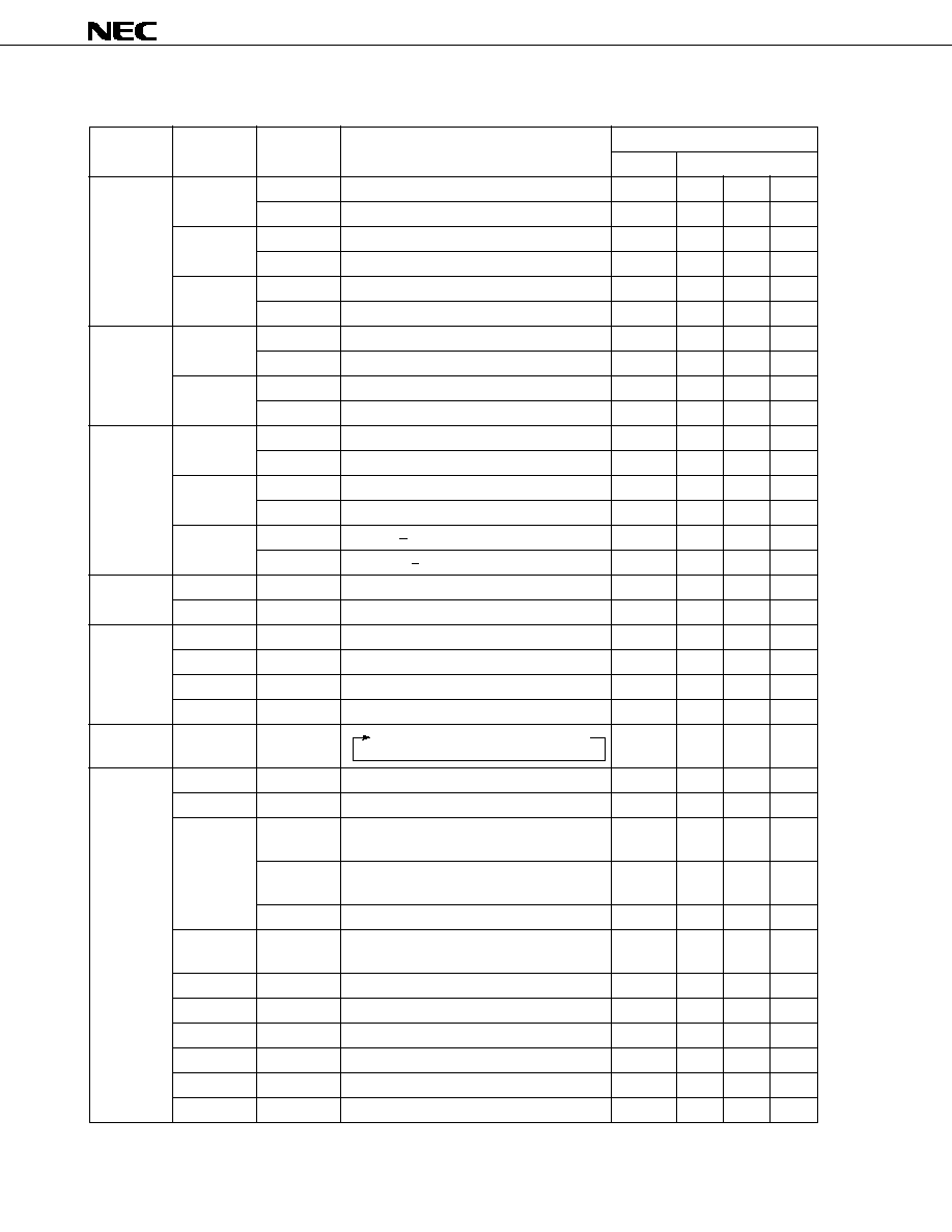
334
�
PD17704, 17705, 17707, 17708, 17709
22.3 Instruction List
Instructions
Mnemonic
Operand
Operation
Instruction Code
Op code
Operand
Add
ADD
r,m
(r)
(r) + (m)
00000
m
R
m
C
r
m,#n4
(m)
(m) + n4
10000
m
R
m
C
n4
ADDC
r,m
(r)
(r) + (m) + CY
00010
m
R
m
C
r
m,#n4
(m)
(m) + n4 + CY
10010
m
R
m
C
n4
INC
AR
AR
AR + 1
00111
000
1001
0000
IX
IX
IX + 1
00111
000
1000
0000
Subtract
SUB
r,m
(r)
(r) � (m)
00001
m
R
m
C
r
m,#n4
(m)
(m) � n4
10001
m
R
m
C
n4
SUBC
r,m
(r)
(r) � (m) � CY
00011
m
R
m
C
r
m,#n4
(m)
(m) � n4 � CY
10011
m
R
m
C
n4
Logical
OR
r,m
(r)
(r) v (m)
00110
m
R
m
C
r
operation
m,#n4
(m)
(m) v n4
10110
m
R
m
C
n4
AND
r,m
(r)
(r) (m)
00100
m
R
m
C
r
m,#n4
(m)
(m) n4
10100
m
R
m
C
n4
XOR
r,m
(r)
(r) v (m)
00101
m
R
m
C
r
m,#n4
(m)
(m) v n4
10101
m
R
m
C
n4
Judge
SKT
m,#n
CMP
0, if (m) n = n, then skip
11110
m
R
m
C
n
SKF
m,#n
CMP
0, if (m) n = 0, then skip
11111
m
R
m
C
n
Compare
SKE
m,#n4
(m) � n4, skip if zero
01001
m
R
m
C
n4
SKNE
m,#n4
(m) � n4, skip if not zero
01011
m
R
m
C
n4
SKGE
m,#n4
(m) � n4, skip if not borrow
11001
m
R
m
C
n4
SKLT
m,#n4
(m) � n4, skip if borrow
11011
m
R
m
C
n4
Rotate
RORC
r
CY
(r) b
3
(r) b
2
(r) b
1
(r) b
0
00111
000
0111
r
Transfer
LD
r,m
(r)
(m)
01000
m
R
m
C
r
ST
m,r
(m)
(r)
11000
m
R
m
C
r
MOV
@r,m
if MPE = 1 : (MP, (r))
(m)
01010
m
R
m
C
r
if MPE = 0 : (BANK, m
R
, (r))
(m)
m, @r
if MPE = 1 : (m)
(MP, (r))
11010
m
R
m
C
r
if MPE = 0 : (m)
(BANK, m
R
, (r))
m,#n4
(m)
n4
11101
m
R
m
C
n4
MOVT
DBF,@AR
SP
SP � 1, ASR
PC, PC
AR,
00111
000
0001
0000
DBF
(PC), PC
ASR, SP
SP + 1
PUSH
AR
SP
SP � 1, ASR
AR
00111
000
1101
0000
POP
AR
AR
ASR, SP
SP + 1
00111
000
1100
0000
GET
DBF,p
DBF
(p)
00111
p
H
1011
p
L
PUT
p,DBF
(p)
DBF
00111
p
H
1010
p
L
PEEK
WR,rf
WR
(rf)
00111
rf
R
0011
rf
C
POKE
rf,WR
(rf)
WR
00111
rf
R
0010
rf
C
v
v
v
v

335
�
PD17704, 17705, 17707, 17708, 17709
Instructions
Mnemonic
Operand
Operation
Instruction Code
Op code
Operand
Branch
BR
addr
PC
10�0
addr, PAGE
0
01100
addr
PC
10�0
addr, PAGE
1
01101
PC
10�0
addr, PAGE
2
01110
PC
10�0
addr, PAGE
3
01111
@AR
PC
AR
00111
000
0100
0000
Subroutine
CALL
addr
SP
SP � 1, ASR
PC
11100
addr
PC
11
0, PC
10�0
addr
@AR
SP
SP � 1, ASR
PC
00111
000
0101
0000
PC
AR
SYSCAL
entry
SP
SP � 1, ASR
PC, SGR
1
00111
entry
H
0010
entry
L
PC
12, 11
0, PC
10�8
entry
H
, PC
7�4
0,
PC
3�0
entry
L
RET
PC
ASR, SP
SP + 1
00111
000
1110
0000
RETSK
PC
ASR, SP
SP + 1 and skip
00111
001
1110
0000
RETI
PC
ASR, INTR
INTSK, SP
SP + 1
00111
010
1110
0000
Interrupt
EI
INTEF
1
00111
000
1111
0000
DI
INTEF
0
00111
001
1111
0000
Others
STOP
s
STOP
00111
010
1111
s
HALT
h
HALT
00111
011
1111
h
NOP
No operation
00111
100
1111
0000
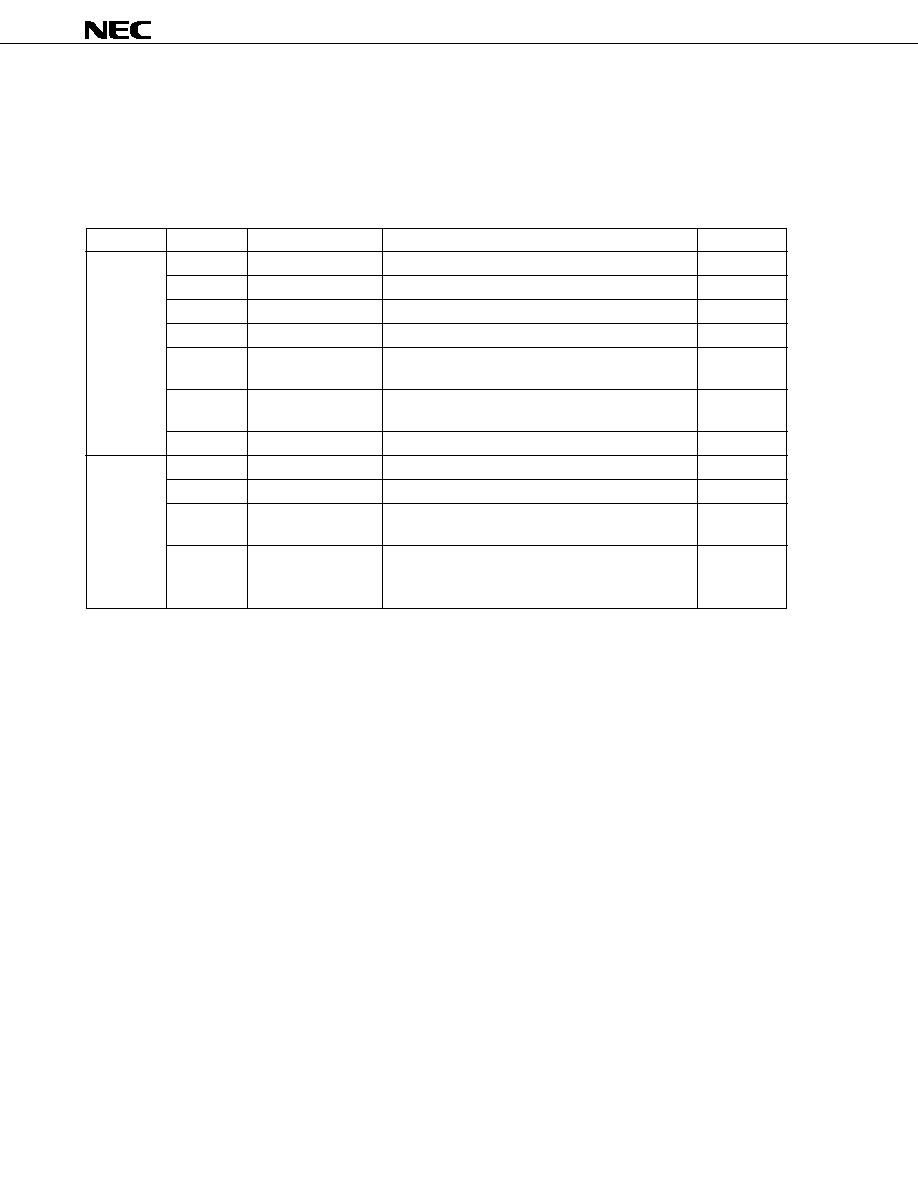
336
�
PD17704, 17705, 17707, 17708, 17709
22.4 Assembler (RA17K) Embedded Macro Instruction
Legend
flag n : FLG symbol
n
: Bit number
< >
: Can be omitted
Mnemonic
Operand
Operation
n
Embedded
SKTn
flag 1, ... flag n
if (flag1) ~ (flag n) = all "1", then skip
1
n
4
macro
SKFn
flag 1, ... flag n
if (flag 1) ~ (flag n) = all "0", then skip
1
n
4
SETn
flag 1, ... flag n
(flag 1) ~ (flag n)
1
1
n
4
CLRn
flag 1, ... flag n
(flag 1) ~ (flag n)
0
1
n
4
NOTn
flag 1, ... flag n
if (flag n) = "0", then (flag n)
1
1
n
4
if (flag n) = "1", then (flag n)
0
INITFLG
<NOT> flag 1,
if description = NOT flag n, then (flag n)
0
1
n
4
... <<NOT> flag n>
if description = flag n, then (flag n)
1
BANKn
(BANK)
n
0
n
15
Expanded
BRX
Label
Jump Label
--
instruction
CALLX
function-name
CALL sub-routine
--
SYSCALX
function-name or
CALL system sub-routine
--
expression
INITFLGX
<NOT/INV> flag 1,
if description = NOT (or INV)
n
4
... <NOT/INV> flag n
flag, (flag)
0
if description = flag, (flag)
1

337
�
PD17704, 17705, 17707, 17708, 17709
23. RESERVED SYMBOLS
23.1 Data Buffer (DBF)
Symbol Name Attribute
Value
R/W
Description
DBF3
MEM
0.0CH
R/W
Bits 15 through 12 of data buffer
DBF2
MEM
0.0DH
R/W
Bits 11 through 8 of data buffer
DBF1
MEM
0.0EH
R/W
Bits 7 through 4 of data buffer
DBF0
MEM
0.0FH
R/W
Bits 3 through 0 of data buffer
23.2 System Registers (SYSREG)
Symbol Name Attribute
Value
R/W
Description
AR3
MEM
0.74H
R/W
Bits 15 through 12 of address register
AR2
MEM
0.75H
R/W
Bits 11 through 8 of address register
AR1
MEM
0.76H
R/W
Bits 7 through 4 of address register
AR0
MEM
0.77H
R/W
Bits 3 through 0 of address register
WR
MEM
0.78H
R/W
Window register
BANK
MEM
0.79H
R/W
Bank register
IXH
MEM
0.7AH
R/W
Bits 10 through 8 of index register
MPH
MEM
0.7AH
R/W
Bits 6 through 4 of memory pointer
MPE
FLG
0.7AH.3
R/W
Memory pointer enable flag
IXM
MEM
0.7BH
R/W
Bits 7 through 4 of index register
MPL
MEM
0.7BH
R/W
Bits 3 through 0 of memory pointer
IXL
MEM
0.7CH
R/W
Bits 3 through 0 of index register
RPH
MEM
0.7DH
R/W
Bits 6 through 3 of general register pointer
RPL
MEM
0.7EH
R/W
Bits 2 through 0 of general register pointer
BCD
FLG
0.7EH.0
R/W
BCD operation flag
PSW
MEM
0.7FH
R/W
Program status word
CMP
FLG
0.7FH.3
R/W
Compare flag
CY
FLG
0.7FH.2
R/W
Carry flag
Z
FLG
0.7FH.1
R/W
Zero flag
IXE
FLG
0.7FH.0
R/W
Index enable flag
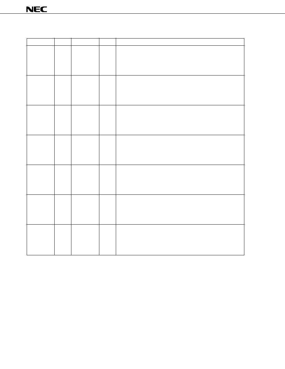
338
�
PD17704, 17705, 17707, 17708, 17709
� � � � � � � � � � � � � � � � � � � � � � � � � � � � � � � � � � � � � � � � � � � � � � � � � � � � � � � � � � � � � � � � � � � � � � � � � � � � � � � � � � � � � � � � � � � � � �
� � � � � � � � � � � � � � � � � � � � � � � � � � � � � � � � � � � � � � � � � � � � � � � � � � � � � � � � � � � � � � � � � � � � � � � � � � � � � � � � � � � � � � � � � � � � � �
� � � � � � � � � � � � � � � � � � � � � � � � � � � � � � � � � � � � � � � � � � � � � � � � � � � � � � � � � � � � � � � � � � � � � � � � � � � � � � � � � � � � � � � � � � � � � �
23.3 Port Registers
Symbol Name Attribute
Value
R/W
Description
P0A3
FLG
0.70H.3
R/W
Bit 3 of port 0A
P0A2
FLG
0.70H.2
R/W
Bit 2 of port 0A
P0A1
FLG
0.70H.1
R/W
Bit 1 of port 0A
P0A0
FLG
0.70H.0
R/W
Bit 0 of port 0A
P0B3
FLG
0.71H.3
R/W
Bit 3 of port 0B
P0B2
FLG
0.71H.2
R/W
Bit 2 of port 0B
P0B1
FLG
0.71H.1
R/W
Bit 1 of port 0B
P0B0
FLG
0.71H.0
R/W
Bit 0 of port 0B
P0C3
FLG
0.72H.3
R/W
Bit 3 of port 0C
P0C2
FLG
0.72H.2
R/W
Bit 2 of port 0C
P0C1
FLG
0.72H.1
R/W
Bit 1 of port 0C
P0C0
FLG
0.72H.0
R/W
Bit 0 of port 0C
P0D3
FLG
0.73H.3
R
Note
Bit 3 of port 0D
P0D2
FLG
0.73H.2
R
Note
Bit 2 of port 0D
P0D1
FLG
0.73H.1
R
Note
Bit 1 of port 0D
P0D0
FLG
0.73H.0
R
Note
Bit 0 of port 0D
P1A3
FLG
1.70H.3
R
Note
Bit 3 of port 1A
P1A2
FLG
1.70H.2
R
Note
Bit 2 of port 1A
P1A1
FLG
1.70H.1
R
Note
Bit 1 of port 1A
P1A0
FLG
1.70H.0
R
Note
Bit 0 of port 1A
P1B3
FLG
1.71H.3
R/W
Bit 3 of port 1B
P1B2
FLG
1.71H.2
R/W
Bit 2 of port 1B
P1B1
FLG
1.71H.1
R/W
Bit 1 of port 1B
P1B0
FLG
1.71H.0
R/W
Bit 0 of port 1B
P1C3
FLG
1.72H.3
R
Note
Bit 3 of port 1C
P1C2
FLG
1.72H.2
R
Note
Bit 2 of port 1C
P1C1
FLG
1.72H.1
R
Note
Bit 1 of port 1C
P1C0
FLG
1.72H.0
R/W
Bit 0 of port 1C
Note
These are input ports. However, even if an instruction that outputs data to these ports is described, the
assembler and in-circuit emulator do not output an error message. Moreover, nothing is affected in terms
of operation even if such an instruction is actually executed on the device.
� � � � � � � � � � � � � � � � � � � � � � � � � � � � � � � � � � � � � � � � � � � � � � � � � � � � � � � � � � � � � � � � � � � � � � � � � � � � � � � � � � � � � � � � � � � � � �
� � � � � � � � � � � � � � � � � � � � � � � � � � � � � � � � � � � � � � � � � � � � � � � � � � � � � � � � � � � � � � � � � � � � � � � � � � � � � � � � � � � � � � � � � � � � � �
� � � � � � � � � � � � � � � � � � � � � � � � � � � � � � � � � � � � � � � � � � � � � � � � � � � � � � � � � � � � � � � � � � � � � � � � � � � � � � � � � � � � � � � � � � � � � �
� � � � � � � � � � � � � � � � � � � � � � � � � � � � � � � � � � � � � � � � � � � � � � � � � � � � � � � � � � � � � � � � � � � � � � � � � � � � � � � � � � � � � � � � � � � � � �
� � � � � � � � � � � � � � � � � � � � � � � � � � � � � � � � � � � � � � � � � � � � � � � � � � � � � � � � � � � � � � � � � � � � � � � � � � � � � � � � � � � � � � � � � � � � � �
� � � � � � � � � � � � � � � � � � � � � � � � � � � � � � � � � � � � � � � � � � � � � � � � � � � � � � � � � � � � � � � � � � � � � � � � � � � � � � � � � � � � � � � � � � � � � �
� � � � � � � � � � � � � � � � � � � � � � � � � � � � � � � � � � � � � � � � � � � � � � � � � � � � � � � � � � � � � � � � � � � � � � � � � � � � � � � � � � � � � � � � � � � � � �
� � � � � � � � � � � � � � � � � � � � � � � � � � � � � � � � � � � � � � � � � � � � � � � � � � � � � � � � � � � � � � � � � � � � � � � � � � � � � � � � � � � � � � � � � � � � � �
� � � � � � � � � � � � � � � � � � � � � � � � � � � � � � � � � � � � � � � � � � � � � � � � � � � � � � � � � � � � � � � � � � � � � � � � � � � � � � � � � � � � � � � � � � � � � �
� � � � � � � � � � � � � � � � � � � � � � � � � � � � � � � � � � � � � � � � � � � � � � � � � � � � � � � � � � � � � � � � � � � � � � � � � � � � � � � � � � � � � � � � � � � � � �
� � � � � � � � � � � � � � � � � � � � � � � � � � � � � � � � � � � � � � � � � � � � � � � � � � � � � � � � � � � � � � � � � � � � � � � � � � � � � � � � � � � � � � � � � � � � � �
� � � � � � � � � � � � � � � � � � � � � � � � � � � � � � � � � � � � � � � � � � � � � � � � � � � � � � � � � � � � � � � � � � � � � � � � � � � � � � � � � � � � � � � � � � � � � �
� � � � � � � � � � � � � � � � � � � � � � � � � � � � � � � � � � � � � � � � � � � � � � � � � � � � � � � � � � � � � � � � � � � � � � � � � � � � � � � � � � � � � � � � � � � � � �
� � � � � � � � � � � � � � � � � � � � � � � � � � � � � � � � � � � � � � � � � � � � � � � � � � � � � � � � � � � � � � � � � � � � � � � � � � � � � � � � � � � � � � � � � � � � � �
� � � � � � � � � � � � � � � � � � � � � � � � � � � � � � � � � � � � � � � � � � � � � � � � � � � � � � � � � � � � � � � � � � � � � � � � � � � � � � � � � � � � � � � � � � � � � �
� � � � � � � � � � � � � � � � � � � � � � � � � � � � � � � � � � � � � � � � � � � � � � � � � � � � � � � � � � � � � � � � � � � � � � � � � � � � � � � � � � � � � � � � � � � � � �
� � � � � � � � � � � � � � � � � � � � � � � � � � � � � � � � � � � � � � � � � � � � � � � � � � � � � � � � � � � � � � � � � � � � � � � � � � � � � � � � � � � � � � � � � � � � � �
� � � � � � � � � � � � � � � � � � � � � � � � � � � � � � � � � � � � � � � � � � � � � � � � � � � � � � � � � � � � � � � � � � � � � � � � � � � � � � � � � � � � � � � � � � � � � �
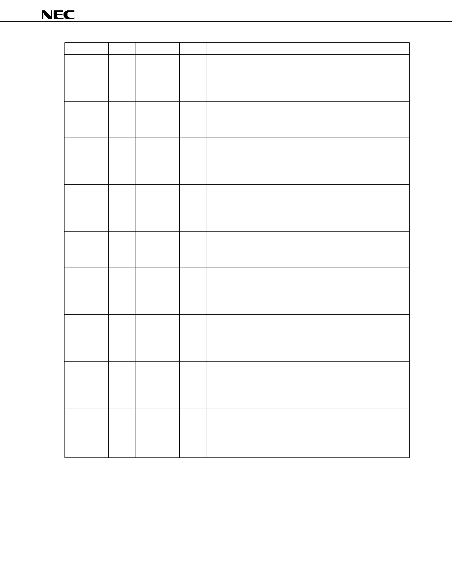
339
�
PD17704, 17705, 17707, 17708, 17709
Symbol Name Attribute
Value
R/W
Description
P1D3
FLG
1.73H.3
R/W
Bit 3 of port 1D
P1D2
FLG
1.73H.2
R/W
Bit 2 of port 1D
P1D1
FLG
1.73H.1
R/W
Bit 1 of port 1D
P1D0
FLG
1.73H.0
R/W
Bit 0 of port 1D
P2A2
FLG
2.70H.2
R/W
Bit 2 of port 2A
P2A1
FLG
2.70H.1
R/W
Bit 1 of port 2A
P2A0
FLG
2.70H.0
R/W
Bit 0 of port 2A
P2B3
FLG
2.71H.3
R/W
Bit 3 of port 2B
P2B2
FLG
2.71H.2
R/W
Bit 2 of port 2B
P2B1
FLG
2.71H.1
R/W
Bit 1 of port 2B
P2B0
FLG
2.71H.0
R/W
Bit 0 of port 2B
P2C3
FLG
2.72H.3
R/W
Bit 3 of port 2C
P2C2
FLG
2.72H.2
R/W
Bit 2 of port 2C
P2C1
FLG
2.72H.1
R/W
Bit 1 of port 2C
P2C0
FLG
2.72H.0
R/W
Bit 0 of port 2C
P2D2
FLG
2.73H.2
R/W
Bit 2 of port 2D
P2D1
FLG
2.73H.1
R/W
Bit 1 of port 2D
P2D0
FLG
2.73H.0
R/W
Bit 0 of port 2D
P3A3
FLG
3.70H.3
R/W
Bit 3 of port 3A
P3A2
FLG
3.70H.2
R/W
Bit 2 of port 3A
P3A1
FLG
3.70H.1
R/W
Bit 1 of port 3A
P3A0
FLG
3.70H.0
R/W
Bit 0 of port 3A
P3B3
FLG
3.71H.3
R/W
Bit 3 of port 3B
P3B2
FLG
3.71H.2
R/W
Bit 2 of port 3B
P3B1
FLG
3.71H.1
R/W
Bit 1 of port 3B
P3B0
FLG
3.71H.0
R/W
Bit 0 of port 3B
P3C3
FLG
3.72H.3
R/W
Bit 3 of port 3C
P3C2
FLG
3.72H.2
R/W
Bit 2 of port 3C
P3C1
FLG
3.72H.1
R/W
Bit 1 of port 3C
P3C0
FLG
3.72H.0
R/W
Bit 0 of port 3C
P3D3
FLG
3.73H.3
R/W
Bit 3 of port 3D
P3D2
FLG
3.72H.2
R/W
Bit 2 of port 3D
P3D1
FLG
3.73H.1
R/W
Bit 1 of port 3D
P3D0
FLG
3.73H.0
R/W
Bit 0 of port 3D
� � � � � � � � � � � � � � � � � � � � � � � � � � � � � � � � � � � � � � � � � � � � � � � � � � � � � � � � � � � � � � � � � � � � � � � � � � � � � � � � � � � � � � � � � � � � � �
� � � � � � � � � � � � � � � � � � � � � � � � � � � � � � � � � � � � � � � � � � � � � � � � � � � � � � � � � � � � � � � � � � � � � � � � � � � � � � � � � � � � � � � � � � � � � �
� � � � � � � � � � � � � � � � � � � � � � � � � � � � � � � � � � � � � � � � � � � � � � � � � � � � � � � � � � � � � � � � � � � � � � � � � � � � � � � � � � � � � � � � � � � � � �
� � � � � � � � � � � � � � � � � � � � � � � � � � � � � � � � � � � � � � � � � � � � � � � � � � � � � � � � � � � � � � � � � � � � � � � � � � � � � � � � � � � � � � � � � � � � � �
� � � � � � � � � � � � � � � � � � � � � � � � � � � � � � � � � � � � � � � � � � � � � � � � � � � � � � � � � � � � � � � � � � � � � � � � � � � � � � � � � � � � � � � � � � � � � �
� � � � � � � � � � � � � � � � � � � � � � � � � � � � � � � � � � � � � � � � � � � � � � � � � � � � � � � � � � � � � � � � � � � � � � � � � � � � � � � � � � � � � � � � � � � � � �
� � � � � � � � � � � � � � � � � � � � � � � � � � � � � � � � � � � � � � � � � � � � � � � � � � � � � � � � � � � � � � � � � � � � � � � � � � � � � � � � � � � � � � � � � � � � � �
� � � � � � � � � � � � � � � � � � � � � � � � � � � � � � � � � � � � � � � � � � � � � � � � � � � � � � � � � � � � � � � � � � � � � � � � � � � � � � � � � � � � � � � � � � � � � �
� � � � � � � � � � � � � � � � � � � � � � � � � � � � � � � � � � � � � � � � � � � � � � � � � � � � � � � � � � � � � � � � � � � � � � � � � � � � � � � � � � � � � � � � � � � � � �
� � � � � � � � � � � � � � � � � � � � � � � � � � � � � � � � � � � � � � � � � � � � � � � � � � � � � � � � � � � � � � � � � � � � � � � � � � � � � � � � � � � � � � � � � � � � � �
� � � � � � � � � � � � � � � � � � � � � � � � � � � � � � � � � � � � � � � � � � � � � � � � � � � � � � � � � � � � � � � � � � � � � � � � � � � � � � � � � � � � � � � � � � � � � �
� � � � � � � � � � � � � � � � � � � � � � � � � � � � � � � � � � � � � � � � � � � � � � � � � � � � � � � � � � � � � � � � � � � � � � � � � � � � � � � � � � � � � � � � � � � � � �
� � � � � � � � � � � � � � � � � � � � � � � � � � � � � � � � � � � � � � � � � � � � � � � � � � � � � � � � � � � � � � � � � � � � � � � � � � � � � � � � � � � � � � � � � � � � � �
� � � � � � � � � � � � � � � � � � � � � � � � � � � � � � � � � � � � � � � � � � � � � � � � � � � � � � � � � � � � � � � � � � � � � � � � � � � � � � � � � � � � � � � � � � � � � �
� � � � � � � � � � � � � � � � � � � � � � � � � � � � � � � � � � � � � � � � � � � � � � � � � � � � � � � � � � � � � � � � � � � � � � � � � � � � � � � � � � � � � � � � � � � � � �
� � � � � � � � � � � � � � � � � � � � � � � � � � � � � � � � � � � � � � � � � � � � � � � � � � � � � � � � � � � � � � � � � � � � � � � � � � � � � � � � � � � � � � � � � � � � � �
� � � � � � � � � � � � � � � � � � � � � � � � � � � � � � � � � � � � � � � � � � � � � � � � � � � � � � � � � � � � � � � � � � � � � � � � � � � � � � � � � � � � � � � � � � � � � �
� � � � � � � � � � � � � � � � � � � � � � � � � � � � � � � � � � � � � � � � � � � � � � � � � � � � � � � � � � � � � � � � � � � � � � � � � � � � � � � � � � � � � � � � � � � � � �
� � � � � � � � � � � � � � � � � � � � � � � � � � � � � � � � � � � � � � � � � � � � � � � � � � � � � � � � � � � � � � � � � � � � � � � � � � � � � � � � � � � � � � � � � � � � � �
� � � � � � � � � � � � � � � � � � � � � � � � � � � � � � � � � � � � � � � � � � � � � � � � � � � � � � � � � � � � � � � � � � � � � � � � � � � � � � � � � � � � � � � � � � � � � �
� � � � � � � � � � � � � � � � � � � � � � � � � � � � � � � � � � � � � � � � � � � � � � � � � � � � � � � � � � � � � � � � � � � � � � � � � � � � � � � � � � � � � � � � � � � � � �
� � � � � � � � � � � � � � � � � � � � � � � � � � � � � � � � � � � � � � � � � � � � � � � � � � � � � � � � � � � � � � � � � � � � � � � � � � � � � � � � � � � � � � � � � � � � � �
� � � � � � � � � � � � � � � � � � � � � � � � � � � � � � � � � � � � � � � � � � � � � � � � � � � � � � � � � � � � � � � � � � � � � � � � � � � � � � � � � � � � � � � � � � � � � �
� � � � � � � � � � � � � � � � � � � � � � � � � � � � � � � � � � � � � � � � � � � � � � � � � � � � � � � � � � � � � � � � � � � � � � � � � � � � � � � � � � � � � � � � � � � � � �
� � � � � � � � � � � � � � � � � � � � � � � � � � � � � � � � � � � � � � � � � � � � � � � � � � � � � � � � � � � � � � � � � � � � � � � � � � � � � � � � � � � � � � � � � � � � � �

340
�
PD17704, 17705, 17707, 17708, 17709
23.4 Register File (Control Registers)
Symbol Name Attribute
Value
R/W
Description
SP
MEM
0.81H
R/W
Stack pointer
WDTCK
MEM
0.82H
R/W
Watchdog timer clock selection flag (can be set only once after power
application)
WDTCK1
FLG
0.82H.1
R/W
Watchdog timer clock selection flag (can be set only once after power
application)
WDTCK0
FLG
0.82H.0
R/W
Watchdog timer clock selection flag (can be set only once after power
application)
WDTRES
FLG
0.83H.3
R/W
Watchdog timer counter reset (when read: 0)
DBFSP
MEM
0.84H
R
DBF stack pointer
SPRSEL
MEM
0.85H
R/W
Stack overflow/underflow reset selection flag (can be set only once after
power application)
ISPRES
FLG
0.85H.1
R/W
Stack overflow/underflow reset selection flag (can be set only once after
power application)
ASPRES
FLG
0.85H.0
R/W
Stack overflow/underflow reset selection flag (can be set only once after
power application)
CECNT3
FLG
0.86H.3
R/W
CE reset timer carry counter
CECNT2
FLG
0.86H.2
R/W
CE reset timer carry counter
CECNT1
FLG
0.86H.1
R/W
CE reset timer carry counter
CECNT0
FLG
0.86H.0
R/W
CE reset timer carry counter
MOVTSEL1
FLG
0.87H.1
R/W
MOVT bit selection flag
MOVTSEL0
FLG
0.87H.0
R/W
MOVT bit selection flag
SYSRSP
MEM
0.88H
R
System register stack pointer
SIO0WSTT
FLG
0.8AH.0
R
Serial interface 0 wait status judgment flag
SBMD
FLG
0.8BH.2
R/W
I
2
C bus slave transmission operation mode selection flag
SIO0CK1
FLG
0.8BH.1
R/W
Serial interface 0 I/O clock selection flag
SIO0CK0
FLG
0.8BH.0
R/W
Serial interface 0 I/O clock selection flag
SIO0IMD3
FLG
0.8CH.3
R/W
Serial interface 0 interrupt mode selection flag (dummy)
SIO0IMD2
FLG
0.8CH.2
R/W
Serial interface 0 interrupt mode selection flag (dummy)
SIO0IMD1
FLG
0.8CH.1
R/W
Serial interface 0 interrupt mode selection flag
SIO0IMD0
FLG
0.8CH.0
R/W
Serial interface 0 interrupt mode selection flag
SIO0SF8
FLG
0.8DH.3
R
8-count detection flag of serial interface 0 clock counter
SIO0SF9
FLG
0.8DH.2
R
9-count detection flag of serial interface 0 clock counter
SBSTT
FLG
0.8DH.1
R
Serial interface 0 (I
2
C mode) communication status detection flag
(1: Start condition detected)
SBBSY
FLG
0.8DH.0
R
Serial interface 0 (I
2
C mode) communication status detection flag
(1: Start condition detected, 0: Stop condition detected)
SBACK
FLG
0.8EH.3
R/W`
Serial interface 0 (I
2
C mode) ACK signal setting/detection flag
SIO0NWT
FLG
0.8EH.2
R/W
Serial interface 0 wait status setting/detection flag
(1: Wait status released (no wait))
SIO0WRQ1
FLG
0.8EH.1
R/W
Bit 1 of serial interface 0 wait condition setting flag
SIO0WRQ0
FLG
0.8EH.0
R/W
Bit 0 of serial interface 0 wait condition setting flag
� � � � � � � � � � � � � � � � � � � � � � � � � � � � � � � � � � � � � � � � � � � � � � � � � � � � � � � � � � � � � � � � � � � � � � � � � � � � � � � � � � � � � � � � � � � � � �
� � � � � � � � � � � � � � � � � � � � � � � � � � � � � � � � � � � � � � � � � � � � � � � � � � � � � � � � � � � � � � � � � � � � � � � � � � � � � � � � � � � � � � � � � � � � � �
� � � � � � � � � � � � � � � � � � � � � � � � � � � � � � � � � � � � � � � � � � � � � � � � � � � � � � � � � � � � � � � � � � � � � � � � � � � � � � � � � � � � � � � � � � � � � �
� � � � � � � � � � � � � � � � � � � � � � � � � � � � � � � � � � � � � � � � � � � � � � � � � � � � � � � � � � � � � � � � � � � � � � � � � � � � � � � � � � � � � � � � � � � � � �
� � � � � � � � � � � � � � � � � � � � � � � � � � � � � � � � � � � � � � � � � � � � � � � � � � � � � � � � � � � � � � � � � � � � � � � � � � � � � � � � � � � � � � � � � � � � � �
� � � � � � � � � � � � � � � � � � � � � � � � � � � � � � � � � � � � � � � � � � � � � � � � � � � � � � � � � � � � � � � � � � � � � � � � � � � � � � � � � � � � � � � � � � � � � �
� � � � � � � � � � � � � � � � � � � � � � � � � � � � � � � � � � � � � � � � � � � � � � � � � � � � � � � � � � � � � � � � � � � � � � � � � � � � � � � � � � � � � � � � � � � � � �
� � � � � � � � � � � � � � � � � � � � � � � � � � � � � � � � � � � � � � � � � � � � � � � � � � � � � � � � � � � � � � � � � � � � � � � � � � � � � � � � � � � � � � � � � � � � � �
� � � � � � � � � � � � � � � � � � � � � � � � � � � � � � � � � � � � � � � � � � � � � � � � � � � � � � � � � � � � � � � � � � � � � � � � � � � � � � � � � � � � � � � � � � � � � �
� � � � � � � � � � � � � � � � � � � � � � � � � � � � � � � � � � � � � � � � � � � � � � � � � � � � � � � � � � � � � � � � � � � � � � � � � � � � � � � � � � � � � � � � � � � � � �
� � � � � � � � � � � � � � � � � � � � � � � � � � � � � � � � � � � � � � � � � � � � � � � � � � � � � � � � � � � � � � � � � � � � � � � � � � � � � � � � � � � � � � � � � � � � � �
� � � � � � � � � � � � � � � � � � � � � � � � � � � � � � � � � � � � � � � � � � � � � � � � � � � � � � � � � � � � � � � � � � � � � � � � � � � � � � � � � � � � � � � � � � � � � �
� � � � � � � � � � � � � � � � � � � � � � � � � � � � � � � � � � � � � � � � � � � � � � � � � � � � � � � � � � � � � � � � � � � � � � � � � � � � � � � � � � � � � � � � � � � � � �
� � � � � � � � � � � � � � � � � � � � � � � � � � � � � � � � � � � � � � � � � � � � � � � � � � � � � � � � � � � � � � � � � � � � � � � � � � � � � � � � � � � � � � � � � � � � � �
� � � � � � � � � � � � � � � � � � � � � � � � � � � � � � � � � � � � � � � � � � � � � � � � � � � � � � � � � � � � � � � � � � � � � � � � � � � � � � � � � � � � � � � � � � � � � �
� � � � � � � � � � � � � � � � � � � � � � � � � � � � � � � � � � � � � � � � � � � � � � � � � � � � � � � � � � � � � � � � � � � � � � � � � � � � � � � � � � � � � � � � � � � � � �
341
�
PD17704, 17705, 17707, 17708, 17709
Symbol Name Attribute
Value
R/W
Description
SIO0CH
FLG
0.8FH.3
R/W
Serial interface 0 mode selection flag
SB
FLG
0.8FH.2
R/W
Serial interface 0 mode selection flag
SIO0MS
FLG
0.8FH.1
R/W
Serial interface 0 shift clock mode selection flag
SIO0TX
FLG
0.8FH.0
R/W
Serial interface 0 transmission (TX)/reception (RX) selection flag
PLLSCNF
FLG
0.90H.3
R/W
Swallow counter least significant bit setting flag
PLLMD1
FLG
0.90H.1
R/W
PLL mode selection flag
PLLMD0
FLG
0.90H.0
R/W
PLL mode selection flag
PLLRFCK3
FLG
0.91H.3
R/W
PLL reference frequency selection flag
PLLRFCK2
FLG
0.91H.2
R/W
PLL reference frequency selection flag
PLLRFCK1
FLG
0.91H.1
R/W
PLL reference frequency selection flag
PLLRFCK0
FLG
0.91H.0
R/W
PLL reference frequency selection flag
PLLUL
FLG
0.92H.0
R&Reset
PLL unlock FF flag
BEEP1SEL
FLG
0.93H.1
R/W
BEEP1/general-purpose port pin function selection flag
BEEP0SEL
FLG
0.93H.0
R/W
BEEP0/general-purpose port pin function selection flag
BEEP1CK1
FLG
0.94H.3
R/W
BEEP1 clock selection flag
BEEP1CK0
FLG
0.94H.2
R/W
BEEP1 clock selection flag
BEEP0CK1
FLG
0.94H.1
R/W
BEEP0 clock selection flag
BEEP0CK0
FLG
0.94H.0
R/W
BEEP0 clock selection flag
WDTCY
FLG
0.96H.0
R
Watchdog timer/stack pointer reset status detection flag
BTM0CY
FLG
0.97H.0
R
Basic timer 0 carry flag
BTM0CK1
FLG
0.98H.1
R/W
Basic timer 0 clock selection flag
BTM0CK0
FLG
0.98H.0
R/W
Basic timer 0 clock selection flag
SIO1TS
FLG
0.9DH.3
R/W
Serial interface 1 transmission/reception start flag
SIO1HIZ
FLG
0.9DH.2
R/W
Serial interface 1/general-purpose port selection flag
SIO1CK1
FLG
0.9DH.1
R/W
Serial interface 1 I/O clock selection flag
SIO1CK0
FLG
0.9DH.0
R/W
Serial interface 1 I/O clock selection flag
IEG4
FLG
0.9EH.3
R/W
Edge direction selection flag for INT4 pin interrupt request detection
INT4SEL
FLG
0.9EH.2
R/W
INT4 pin interrupt request flag setting disable
IEG3
FLG
0.9EH.1
R/W
Edge direction selection flag for INT3 pin interrupt request detection
INT3SEL
FLG
0.9EH.0
R/W
INT3 pin interrupt request flag setting disable
IEG2
FLG
0.9FH.2
R/W
Edge direction selection flag for INT2 pin interrupt request detection
IEG1
FLG
0.9FH.1
R/W
Edge direction selection flag for INT1 pin interrupt request detection
IEG0
FLG
0.9FH.0
R/W
Edge direction selection flag for INT0 pin interrupt request detection
FCGCH1
FLG
0.0A0H.1
R/W
FGC channel selection flag
FCGCH0
FLG
0.0A0H.0
R/W
FGC channel selection flag
IFCGOSTT
FLG
0.0A1H.0
R
IF counter gate status detection flag (1: Open, 0: Closed)
� � � � � � � � � � � � � � � � � � � � � � � � � � � � � � � � � � � � � � � � � � � � � � � � � � � � � � � � � � � � � � � � � � � � � � � � � � � � � � � � � � � � � � � � � � � � � �
� � � � � � � � � � � � � � � � � � � � � � � � � � � � � � � � � � � � � � � � � � � � � � � � � � � � � � � � � � � � � � � � � � � � � � � � � � � � � � � � � � � � � � � � � � � � � �
� � � � � � � � � � � � � � � � � � � � � � � � � � � � � � � � � � � � � � � � � � � � � � � � � � � � � � � � � � � � � � � � � � � � � � � � � � � � � � � � � � � � � � � � � � � � � �
� � � � � � � � � � � � � � � � � � � � � � � � � � � � � � � � � � � � � � � � � � � � � � � � � � � � � � � � � � � � � � � � � � � � � � � � � � � � � � � � � � � � � � � � � � � � � �
� � � � � � � � � � � � � � � � � � � � � � � � � � � � � � � � � � � � � � � � � � � � � � � � � � � � � � � � � � � � � � � � � � � � � � � � � � � � � � � � � � � � � � � � � � � � � �
� � � � � � � � � � � � � � � � � � � � � � � � � � � � � � � � � � � � � � � � � � � � � � � � � � � � � � � � � � � � � � � � � � � � � � � � � � � � � � � � � � � � � � � � � � � � � �
� � � � � � � � � � � � � � � � � � � � � � � � � � � � � � � � � � � � � � � � � � � � � � � � � � � � � � � � � � � � � � � � � � � � � � � � � � � � � � � � � � � � � � � � � � � � � �
� � � � � � � � � � � � � � � � � � � � � � � � � � � � � � � � � � � � � � � � � � � � � � � � � � � � � � � � � � � � � � � � � � � � � � � � � � � � � � � � � � � � � � � � � � � � � �
� � � � � � � � � � � � � � � � � � � � � � � � � � � � � � � � � � � � � � � � � � � � � � � � � � � � � � � � � � � � � � � � � � � � � � � � � � � � � � � � � � � � � � � � � � � � � �
� � � � � � � � � � � � � � � � � � � � � � � � � � � � � � � � � � � � � � � � � � � � � � � � � � � � � � � � � � � � � � � � � � � � � � � � � � � � � � � � � � � � � � � � � � � � � �
� � � � � � � � � � � � � � � � � � � � � � � � � � � � � � � � � � � � � � � � � � � � � � � � � � � � � � � � � � � � � � � � � � � � � � � � � � � � � � � � � � � � � � � � � � � � � �
� � � � � � � � � � � � � � � � � � � � � � � � � � � � � � � � � � � � � � � � � � � � � � � � � � � � � � � � � � � � � � � � � � � � � � � � � � � � � � � � � � � � � � � � � � � � � �
� � � � � � � � � � � � � � � � � � � � � � � � � � � � � � � � � � � � � � � � � � � � � � � � � � � � � � � � � � � � � � � � � � � � � � � � � � � � � � � � � � � � � � � � � � � � � �
� � � � � � � � � � � � � � � � � � � � � � � � � � � � � � � � � � � � � � � � � � � � � � � � � � � � � � � � � � � � � � � � � � � � � � � � � � � � � � � � � � � � � � � � � � � � � �
� � � � � � � � � � � � � � � � � � � � � � � � � � � � � � � � � � � � � � � � � � � � � � � � � � � � � � � � � � � � � � � � � � � � � � � � � � � � � � � � � � � � � � � � � � � � � �
� � � � � � � � � � � � � � � � � � � � � � � � � � � � � � � � � � � � � � � � � � � � � � � � � � � � � � � � � � � � � � � � � � � � � � � � � � � � � � � � � � � � � � � � � � � � � �
� � � � � � � � � � � � � � � � � � � � � � � � � � � � � � � � � � � � � � � � � � � � � � � � � � � � � � � � � � � � � � � � � � � � � � � � � � � � � � � � � � � � � � � � � � � � � �
� � � � � � � � � � � � � � � � � � � � � � � � � � � � � � � � � � � � � � � � � � � � � � � � � � � � � � � � � � � � � � � � � � � � � � � � � � � � � � � � � � � � � � � � � � � � � �
� � � � � � � � � � � � � � � � � � � � � � � � � � � � � � � � � � � � � � � � � � � � � � � � � � � � � � � � � � � � � � � � � � � � � � � � � � � � � � � � � � � � � � � � � � � � � �
� � � � � � � � � � � � � � � � � � � � � � � � � � � � � � � � � � � � � � � � � � � � � � � � � � � � � � � � � � � � � � � � � � � � � � � � � � � � � � � � � � � � � � � � � � � � � �
� � � � � � � � � � � � � � � � � � � � � � � � � � � � � � � � � � � � � � � � � � � � � � � � � � � � � � � � � � � � � � � � � � � � � � � � � � � � � � � � � � � � � � � � � � � � � �
� � � � � � � � � � � � � � � � � � � � � � � � � � � � � � � � � � � � � � � � � � � � � � � � � � � � � � � � � � � � � � � � � � � � � � � � � � � � � � � � � � � � � � � � � � � � � �

342
�
PD17704, 17705, 17707, 17708, 17709
Symbol Name Attribute
Value
R/W
Description
IFCMD1
FLG
0.0A2H.3
R/W
IF counter mode selection flag (10: AMIF, 11: FCG)
IFCMD0
FLG
0.0A2H.2
R/W
IF counter mode selection flag (00: CGP, 11: FMIF)
IFCCK1
FLG
0.0A2H.1
R/W
IF counter clock selection flag
IFCCK0
FLG
0.0A2H.0
R/W
IF counter clock selection flag
IFCSTRT
FLG
0.0A3H.1
W
IF counter count start flag
IFCRES
FLG
0.0A3H.0
W
IF counter reset flag
ADCCH3
FLG
0.0A4H.3
R/W
A/D converter channel selection flag (dummy)
ADCCH2
FLG
0.0A4H.2
R/W
A/D converter channel selection flag
ADCCH1
FLG
0.0A4H.1
R/W
A/D converter channel selection flag
ADCCH0
FLG
0.0A4H.0
R/W
A/D converter channel selection flag
ADCMD
FLG
0.0A5H.2
R/W
A/D converter compare mode selection flag
ADCSTT
FLG
0.0A5H.1
R
A/D converter operation status detection flag (0: End of conversion, 1:
Conversion in progress)
ADCCMP
FLG
0.0A5H.0
R
A/D converter compare result detection flag
PWMBIT
FLG
0.0A6H.2
R/W
PWM counter bit selection flag (0: 8 bits, 1: 9 bits)
PWMCK
FLG
0.0A6H.0
R/W
PWM timer output clock selection flag
PWM2SEL
FLG
0.0A7H.2
R/W
PWM2/general-purpose port pin function selection flag
PWM1SEL
FLG
0.0A7H.1
R/W
PWM1/general-purpose port pin function selection flag
PWM0SEL
FLG
0.0A7H.0
R/W
PWM0/general-purpose port pin function selection flag
TM3SEL
FLG
0.0A8H.3
R/W
PWM/modulo timer 3 selection flag
TM3EN
FLG
0.0A8H.1
R/W
Modulo timer 3 count start flag
TM3RES
FLG
0.0A8H.0
R/W
Modulo timer 3 reset flag (when read: 0)
TM2EN
FLG
0.0A9H.3
R/W
Modulo timer 2 count start flag
TM2RES
FLG
0.0A9H.2
R/W
Modulo timer 2 reset flag (when read: 0)
TM2CK1
FLG
0.0A9H.1
R/W
Modulo timer 2 clock selection flag
TM2CK0
FLG
0.0A9H.0
R/W
Modulo timer 2 clock selection flag
TM1EN
FLG
0.0AAH.3
R/W
Modulo timer 1 count start flag
TM1RES
FLG
0.0AAH.2
R/W
Modulo timer 1 reset flag (when read: 0)
TM1CK1
FLG
0.0AAH.1
R/W
Modulo timer 1 clock selection flag
TM1CK0
FLG
0.0AAH.0
R/W
Modulo timer 1 clock selection flag
TM0EN
FLG
0.0ABH.3
R/W
Modulo timer 0 count start flag
TM0RES
FLG
0.0ABH.2
R/W
Modulo timer 0 reset flag (when read: 0)
TM0CK1
FLG
0.0ABH.1
R/W
Modulo timer 0 clock selection flag
TM0CK0
FLG
0.0ABH.0
R/W
Modulo timer 0 clock selection flag
TM0OVF
FLG
0.0ACH.3
R
Modulo timer 0 overflow detection flag
TM0GCEG
FLG
0.0ACH.2
R/W
Modulo timer 0 gate close input signal edge selection flag
TM0GOEG
FLG
0.0ACH.1
R/W
Modulo timer 0 gate open input signal edge selection flag
TM0MD
FLG
0.0ACH.0
R/W
Modulo timer 0 modulo counter/gate counter selection flag
� � � � � � � � � � � � � � � � � � � � � � � � � � � � � � � � � � � � � � � � � � � � � � � � � � � � � � � � � � � � � � � � � � � � � � � � � � � � � � � � � � � � � � � � � � � � � �
� � � � � � � � � � � � � � � � � � � � � � � � � � � � � � � � � � � � � � � � � � � � � � � � � � � � � � � � � � � � � � � � � � � � � � � � � � � � � � � � � � � � � � � � � � � � � �
� � � � � � � � � � � � � � � � � � � � � � � � � � � � � � � � � � � � � � � � � � � � � � � � � � � � � � � � � � � � � � � � � � � � � � � � � � � � � � � � � � � � � � � � � � � � � �
� � � � � � � � � � � � � � � � � � � � � � � � � � � � � � � � � � � � � � � � � � � � � � � � � � � � � � � � � � � � � � � � � � � � � � � � � � � � � � � � � � � � � � � � � � � � � �
� � � � � � � � � � � � � � � � � � � � � � � � � � � � � � � � � � � � � � � � � � � � � � � � � � � � � � � � � � � � � � � � � � � � � � � � � � � � � � � � � � � � � � � � � � � � � �
� � � � � � � � � � � � � � � � � � � � � � � � � � � � � � � � � � � � � � � � � � � � � � � � � � � � � � � � � � � � � � � � � � � � � � � � � � � � � � � � � � � � � � � � � � � � � �
� � � � � � � � � � � � � � � � � � � � � � � � � � � � � � � � � � � � � � � � � � � � � � � � � � � � � � � � � � � � � � � � � � � � � � � � � � � � � � � � � � � � � � � � � � � � � �
� � � � � � � � � � � � � � � � � � � � � � � � � � � � � � � � � � � � � � � � � � � � � � � � � � � � � � � � � � � � � � � � � � � � � � � � � � � � � � � � � � � � � � � � � � � � � �
� � � � � � � � � � � � � � � � � � � � � � � � � � � � � � � � � � � � � � � � � � � � � � � � � � � � � � � � � � � � � � � � � � � � � � � � � � � � � � � � � � � � � � � � � � � � � �
� � � � � � � � � � � � � � � � � � � � � � � � � � � � � � � � � � � � � � � � � � � � � � � � � � � � � � � � � � � � � � � � � � � � � � � � � � � � � � � � � � � � � � � � � � � � � �
� � � � � � � � � � � � � � � � � � � � � � � � � � � � � � � � � � � � � � � � � � � � � � � � � � � � � � � � � � � � � � � � � � � � � � � � � � � � � � � � � � � � � � � � � � � � � �
� � � � � � � � � � � � � � � � � � � � � � � � � � � � � � � � � � � � � � � � � � � � � � � � � � � � � � � � � � � � � � � � � � � � � � � � � � � � � � � � � � � � � � � � � � � � � �
� � � � � � � � � � � � � � � � � � � � � � � � � � � � � � � � � � � � � � � � � � � � � � � � � � � � � � � � � � � � � � � � � � � � � � � � � � � � � � � � � � � � � � � � � � � � � �
� � � � � � � � � � � � � � � � � � � � � � � � � � � � � � � � � � � � � � � � � � � � � � � � � � � � � � � � � � � � � � � � � � � � � � � � � � � � � � � � � � � � � � � � � � � � � �
� � � � � � � � � � � � � � � � � � � � � � � � � � � � � � � � � � � � � � � � � � � � � � � � � � � � � � � � � � � � � � � � � � � � � � � � � � � � � � � � � � � � � � � � � � � � � �
� � � � � � � � � � � � � � � � � � � � � � � � � � � � � � � � � � � � � � � � � � � � � � � � � � � � � � � � � � � � � � � � � � � � � � � � � � � � � � � � � � � � � � � � � � � � � �
� � � � � � � � � � � � � � � � � � � � � � � � � � � � � � � � � � � � � � � � � � � � � � � � � � � � � � � � � � � � � � � � � � � � � � � � � � � � � � � � � � � � � � � � � � � � � �
� � � � � � � � � � � � � � � � � � � � � � � � � � � � � � � � � � � � � � � � � � � � � � � � � � � � � � � � � � � � � � � � � � � � � � � � � � � � � � � � � � � � � � � � � � � � � �
� � � � � � � � � � � � � � � � � � � � � � � � � � � � � � � � � � � � � � � � � � � � � � � � � � � � � � � � � � � � � � � � � � � � � � � � � � � � � � � � � � � � � � � � � � � � � �
� � � � � � � � � � � � � � � � � � � � � � � � � � � � � � � � � � � � � � � � � � � � � � � � � � � � � � � � � � � � � � � � � � � � � � � � � � � � � � � � � � � � � � � � � � � � � �
� � � � � � � � � � � � � � � � � � � � � � � � � � � � � � � � � � � � � � � � � � � � � � � � � � � � � � � � � � � � � � � � � � � � � � � � � � � � � � � � � � � � � � � � � � � � � �
� � � � � � � � � � � � � � � � � � � � � � � � � � � � � � � � � � � � � � � � � � � � � � � � � � � � � � � � � � � � � � � � � � � � � � � � � � � � � � � � � � � � � � � � � � � � � �
� � � � � � � � � � � � � � � � � � � � � � � � � � � � � � � � � � � � � � � � � � � � � � � � � � � � � � � � � � � � � � � � � � � � � � � � � � � � � � � � � � � � � � � � � � � � � �
� � � � � � � � � � � � � � � � � � � � � � � � � � � � � � � � � � � � � � � � � � � � � � � � � � � � � � � � � � � � � � � � � � � � � � � � � � � � � � � � � � � � � � � � � � � � � �
� � � � � � � � � � � � � � � � � � � � � � � � � � � � � � � � � � � � � � � � � � � � � � � � � � � � � � � � � � � � � � � � � � � � � � � � � � � � � � � � � � � � � � � � � � � � � �
� � � � � � � � � � � � � � � � � � � � � � � � � � � � � � � � � � � � � � � � � � � � � � � � � � � � � � � � � � � � � � � � � � � � � � � � � � � � � � � � � � � � � � � � � � � � � �
343
�
PD17704, 17705, 17707, 17708, 17709
� � � � � � � � � � � � � � � � � � � � � � � � � � � � � � � � � � � � � � � � � � � � � � � � � � � � � � � � � � � � � � � � � � � � � � � � � � � � � � � � � � � � � � � � � � � � � �
� � � � � � � � � � � � � � � � � � � � � � � � � � � � � � � � � � � � � � � � � � � � � � � � � � � � � � � � � � � � � � � � � � � � � � � � � � � � � � � � � � � � � � � � � � � � � �
� � � � � � � � � � � � � � � � � � � � � � � � � � � � � � � � � � � � � � � � � � � � � � � � � � � � � � � � � � � � � � � � � � � � � � � � � � � � � � � � � � � � � � � � � � � � � �
Symbol Name Attribute
Value
R/W
Description
IPSIO1
FLG
0.0ADH.3
R/W
Serial interface 1 interrupt enable flag
IPSIO0
FLG
0.0ADH.2
R/W
Serial interface 0 interrupt enable flag
IPTM3
FLG
0.0ADH.1
R/W
PWM timer interrupt enable flag
IPTM2
FLG
0.0ADH.0
R/W
Modulo timer 2 interrupt enable flag
IPTM1
FLG
0.0AEH.3
R/W
Modulo timer 1 interrupt enable flag
IPTM0
FLG
0.0AEH.2
R/W
Modulo timer 0 interrupt enable flag
IP4
FLG
0.0AEH.1
R/W
INT4 pin interrupt enable flag
IP3
FLG
0.0AEH.0
R/W
INT3 pin interrupt enable flag
IP2
FLG
0.0AFH.3
R/W
INT2 pin interrupt enable flag
IP1
FLG
0.0AFH.2
R/W
INT1 pin interrupt enable flag
IP0
FLG
0.0AFH.1
R/W
INT0 pin interrupt enable flag
IPCE
FLG
0.0AFH.0
R/W
CE pin interrupt enable flag
IRQSIO1
FLG
0.0B4H.0
R/W
Serial interface 1 interrupt request detection flag
IRQSIO0
FLG
0.0B5H.0
R/W
Serial interface 0 interrupt request detection flag
IRQTM3
FLG
0.0B6H.0
R/W
PWM timer interrupt request detection flag
IRQTM2
FLG
0.0B7H.0
R/W
Modulo timer 2 interrupt request detection flag
IRQTM1
FLG
0.0B8H.0
R/W
Modulo timer 1 interrupt request detection flag
IRQTM0
FLG
0.0B9H.0
R/W
Modulo timer 0 interrupt request detection flag
INT4
FLG
0.0BAH.3
R
INT4 pin status detection flag
IRQ4
FLG
0.0BAH.0
R/W
INT4 pin interrupt request detection flag
INT3
FLG
0.0BBH.3
R
INT3 pin status detection flag
IRQ3
FLG
0.0BBH.0
R/W
INT3 pin interrupt request detection flag
INT2
FLG
0.0BCH.3
R
INT2 pin status detection flag
IRQ2
FLG
0.0BCH.0
R/W
INT2 pin interrupt request detection flag
INT1
FLG
0.0BDH.3
R
INT1 pin status detection flag
IRQ1
FLG
0.0BDH.0
R/W
INT1 pin interrupt request detection flag
INT0
FLG
0.0BEH.3
R
INT0 pin status detection flag
IRQ0
FLG
0.0BEH.0
R/W
INT0 pin interrupt request detection flag
CE
FLG
0.0BFH.3
R
CE pin status detection flag
CECNTSTT
FLG
0.0BFH.1
R
CE reset counter status detection flag
IRQCE
FLG
0.0BFH.0
R/W
CE pin interrupt request detection flag
P0DPLD3
FLG
15.66H.3
R/W
P0D3 pin pull-down resistor selection flag
P0DPLD2
FLG
15.66H.2
R/W
P0D2 pin pull-down resistor selection flag
P0DPLD1
FLG
15.66H.1
R/W
P0D1 pin pull-down resistor selection flag
P0DPLD0
FLG
15.66H.0
R/W
P0D0 pin pull-down resistor selection flag
� � � � � � � � � � � � � � � � � � � � � � � � � � � � � � � � � � � � � � � � � � � � � � � � � � � � � � � � � � � � � � � � � � � � � � � � � � � � � � � � � � � � � � � � � � � � � �
� � � � � � � � � � � � � � � � � � � � � � � � � � � � � � � � � � � � � � � � � � � � � � � � � � � � � � � � � � � � � � � � � � � � � � � � � � � � � � � � � � � � � � � � � � � � � �
� � � � � � � � � � � � � � � � � � � � � � � � � � � � � � � � � � � � � � � � � � � � � � � � � � � � � � � � � � � � � � � � � � � � � � � � � � � � � � � � � � � � � � � � � � � � � �
� � � � � � � � � � � � � � � � � � � � � � � � � � � � � � � � � � � � � � � � � � � � � � � � � � � � � � � � � � � � � � � � � � � � � � � � � � � � � � � � � � � � � � � � � � � � � �
� � � � � � � � � � � � � � � � � � � � � � � � � � � � � � � � � � � � � � � � � � � � � � � � � � � � � � � � � � � � � � � � � � � � � � � � � � � � � � � � � � � � � � � � � � � � � �
� � � � � � � � � � � � � � � � � � � � � � � � � � � � � � � � � � � � � � � � � � � � � � � � � � � � � � � � � � � � � � � � � � � � � � � � � � � � � � � � � � � � � � � � � � � � � �
� � � � � � � � � � � � � � � � � � � � � � � � � � � � � � � � � � � � � � � � � � � � � � � � � � � � � � � � � � � � � � � � � � � � � � � � � � � � � � � � � � � � � � � � � � � � � �
� � � � � � � � � � � � � � � � � � � � � � � � � � � � � � � � � � � � � � � � � � � � � � � � � � � � � � � � � � � � � � � � � � � � � � � � � � � � � � � � � � � � � � � � � � � � � �
� � � � � � � � � � � � � � � � � � � � � � � � � � � � � � � � � � � � � � � � � � � � � � � � � � � � � � � � � � � � � � � � � � � � � � � � � � � � � � � � � � � � � � � � � � � � � �
� � � � � � � � � � � � � � � � � � � � � � � � � � � � � � � � � � � � � � � � � � � � � � � � � � � � � � � � � � � � � � � � � � � � � � � � � � � � � � � � � � � � � � � � � � � � � �
� � � � � � � � � � � � � � � � � � � � � � � � � � � � � � � � � � � � � � � � � � � � � � � � � � � � � � � � � � � � � � � � � � � � � � � � � � � � � � � � � � � � � � � � � � � � � �
� � � � � � � � � � � � � � � � � � � � � � � � � � � � � � � � � � � � � � � � � � � � � � � � � � � � � � � � � � � � � � � � � � � � � � � � � � � � � � � � � � � � � � � � � � � � � �
� � � � � � � � � � � � � � � � � � � � � � � � � � � � � � � � � � � � � � � � � � � � � � � � � � � � � � � � � � � � � � � � � � � � � � � � � � � � � � � � � � � � � � � � � � � � � �
� � � � � � � � � � � � � � � � � � � � � � � � � � � � � � � � � � � � � � � � � � � � � � � � � � � � � � � � � � � � � � � � � � � � � � � � � � � � � � � � � � � � � � � � � � � � � �
� � � � � � � � � � � � � � � � � � � � � � � � � � � � � � � � � � � � � � � � � � � � � � � � � � � � � � � � � � � � � � � � � � � � � � � � � � � � � � � � � � � � � � � � � � � � � �
� � � � � � � � � � � � � � � � � � � � � � � � � � � � � � � � � � � � � � � � � � � � � � � � � � � � � � � � � � � � � � � � � � � � � � � � � � � � � � � � � � � � � � � � � � � � � �
344
�
PD17704, 17705, 17707, 17708, 17709
� � � � � � � � � � � � � � � � � � � � � � � � � � � � � � � � � � � � � � � � � � � � � � � � � � � � � � � � � � � � � � � � � � � � � � � � � � � � � � � � � � � � � � � � � � � � � �
� � � � � � � � � � � � � � � � � � � � � � � � � � � � � � � � � � � � � � � � � � � � � � � � � � � � � � � � � � � � � � � � � � � � � � � � � � � � � � � � � � � � � � � � � � � � � �
� � � � � � � � � � � � � � � � � � � � � � � � � � � � � � � � � � � � � � � � � � � � � � � � � � � � � � � � � � � � � � � � � � � � � � � � � � � � � � � � � � � � � � � � � � � � � �
� � � � � � � � � � � � � � � � � � � � � � � � � � � � � � � � � � � � � � � � � � � � � � � � � � � � � � � � � � � � � � � � � � � � � � � � � � � � � � � � � � � � � � � � � � � � � �
� � � � � � � � � � � � � � � � � � � � � � � � � � � � � � � � � � � � � � � � � � � � � � � � � � � � � � � � � � � � � � � � � � � � � � � � � � � � � � � � � � � � � � � � � � � � � �
� � � � � � � � � � � � � � � � � � � � � � � � � � � � � � � � � � � � � � � � � � � � � � � � � � � � � � � � � � � � � � � � � � � � � � � � � � � � � � � � � � � � � � � � � � � � � �
Symbol Name Attribute
Value
R/W
Description
P3DGIO
FLG
15.67H.3
R/W
P3D input/output selection flag
P3CGIO
FLG
15.67H.2
R/W
P3C input/output selection flag
P3BGIO
FLG
15.67H.1
R/W
P3B input/output selection flag
P3AGIO
FLG
15.67H.0
R/W
P3A input/output selection flag
P2DBIO3
FLG
15.68H.3
R/W
P2D3 input/output selection flag (dummy)
P2DBIO2
FLG
15.68H.2
R/W
P2D2 input/output selection flag
P2DBIO1
FLG
15.68H.1
R/W
P2D1 input/output selection flag
P2DBIO0
FLG
15.68H.0
R/W
P2D0 input/output selection flag
P2CBIO3
FLG
15.69H.3
R/W
P2C3 input/output selection flag
P2CBIO2
FLG
15.69H.2
R/W
P2C2 input/output selection flag
P2CBIO1
FLG
15.69H.1
R/W
P2C1 input/output selection flag
P2CBIO0
FLG
15.69H.0
R/W
P2C0 input/output selection flag
P2BBIO3
FLG
15.6AH.3
R/W
P2B3 input/output selection flag
P2BBIO2
FLG
15.6AH.2
R/W
P2B2 input/output selection flag
P2BBIO1
FLG
15.6AH.1
R/W
P2B1 input/output selection flag
P2BBIO0
FLG
15.6AH.0
R/W
P2B0 input/output selection flag
P2ABIO3
FLG
15.6BH.3
R/W
P2A3 input/output selection flag (dummy)
P2ABIO2
FLG
15.6BH.2
R/W
P2A2 input/output selection flag
P2ABIO1
FLG
15.6BH.1
R/W
P2A1 input/output selection flag
P2ABIO0
FLG
15.6BH.0
R/W
P2A0 input/output selection flag
P1DBIO3
FLG
15.6CH.3
R/W
P1D3 input/output selection flag
P1DBIO2
FLG
15.6CH.2
R/W
P1D2 input/output selection flag
P1DBIO1
FLG
15.6CH.1
R/W
P1D1 input/output selection flag
P1DBIO0
FLG
15.6CH.0
R/W
P1D0 input/output selection flag
P0CBIO3
FLG
15.6DH.3
R/W
P0C3 input/output selection flag
P0CBIO2
FLG
15.6DH.2
R/W
P0C2 input/output selection flag
P0CBIO1
FLG
15.6DH.1
R/W
P0C1 input/output selection flag
P0CBIO0
FLG
15.6DH.0
R/W
P0C0 input/output selection flag
P0BBIO3
FLG
15.6EH.3
R/W
P0B3 input/output selection flag
P0BBIO2
FLG
15.6EH.2
R/W
P0B2 input/output selection flag
P0BBIO1
FLG
15.6EH.1
R/W
P0B1 input/output selection flag
P0BBIO0
FLG
15.6EH.0
R/W
P0B0 input/output selection flag
P0ABIO3
FLG
15.6FH.3
R/W
P0A3 input/output selection flag
P0ABIO2
FLG
15.6FH.2
R/W
P0A2 input/output selection flag
P0ABIO1
FLG
15.6FH.1
R/W
P0A1 input/output selection flag
P0ABIO0
FLG
15.6FH.0
R/W
P0A0 input/output selection flag
� � � � � � � � � � � � � � � � � � � � � � � � � � � � � � � � � � � � � � � � � � � � � � � � � � � � � � � � � � � � � � � � � � � � � � � � � � � � � � � � � � � � � � � � � � � � � �
� � � � � � � � � � � � � � � � � � � � � � � � � � � � � � � � � � � � � � � � � � � � � � � � � � � � � � � � � � � � � � � � � � � � � � � � � � � � � � � � � � � � � � � � � � � � � �
� � � � � � � � � � � � � � � � � � � � � � � � � � � � � � � � � � � � � � � � � � � � � � � � � � � � � � � � � � � � � � � � � � � � � � � � � � � � � � � � � � � � � � � � � � � � � �
� � � � � � � � � � � � � � � � � � � � � � � � � � � � � � � � � � � � � � � � � � � � � � � � � � � � � � � � � � � � � � � � � � � � � � � � � � � � � � � � � � � � � � � � � � � � � �
� � � � � � � � � � � � � � � � � � � � � � � � � � � � � � � � � � � � � � � � � � � � � � � � � � � � � � � � � � � � � � � � � � � � � � � � � � � � � � � � � � � � � � � � � � � � � �
� � � � � � � � � � � � � � � � � � � � � � � � � � � � � � � � � � � � � � � � � � � � � � � � � � � � � � � � � � � � � � � � � � � � � � � � � � � � � � � � � � � � � � � � � � � � � �
� � � � � � � � � � � � � � � � � � � � � � � � � � � � � � � � � � � � � � � � � � � � � � � � � � � � � � � � � � � � � � � � � � � � � � � � � � � � � � � � � � � � � � � � � � � � � �
� � � � � � � � � � � � � � � � � � � � � � � � � � � � � � � � � � � � � � � � � � � � � � � � � � � � � � � � � � � � � � � � � � � � � � � � � � � � � � � � � � � � � � � � � � � � � �
� � � � � � � � � � � � � � � � � � � � � � � � � � � � � � � � � � � � � � � � � � � � � � � � � � � � � � � � � � � � � � � � � � � � � � � � � � � � � � � � � � � � � � � � � � � � � �
� � � � � � � � � � � � � � � � � � � � � � � � � � � � � � � � � � � � � � � � � � � � � � � � � � � � � � � � � � � � � � � � � � � � � � � � � � � � � � � � � � � � � � � � � � � � � �
� � � � � � � � � � � � � � � � � � � � � � � � � � � � � � � � � � � � � � � � � � � � � � � � � � � � � � � � � � � � � � � � � � � � � � � � � � � � � � � � � � � � � � � � � � � � � �
� � � � � � � � � � � � � � � � � � � � � � � � � � � � � � � � � � � � � � � � � � � � � � � � � � � � � � � � � � � � � � � � � � � � � � � � � � � � � � � � � � � � � � � � � � � � � �
� � � � � � � � � � � � � � � � � � � � � � � � � � � � � � � � � � � � � � � � � � � � � � � � � � � � � � � � � � � � � � � � � � � � � � � � � � � � � � � � � � � � � � � � � � � � � �
� � � � � � � � � � � � � � � � � � � � � � � � � � � � � � � � � � � � � � � � � � � � � � � � � � � � � � � � � � � � � � � � � � � � � � � � � � � � � � � � � � � � � � � � � � � � � �
� � � � � � � � � � � � � � � � � � � � � � � � � � � � � � � � � � � � � � � � � � � � � � � � � � � � � � � � � � � � � � � � � � � � � � � � � � � � � � � � � � � � � � � � � � � � � �
� � � � � � � � � � � � � � � � � � � � � � � � � � � � � � � � � � � � � � � � � � � � � � � � � � � � � � � � � � � � � � � � � � � � � � � � � � � � � � � � � � � � � � � � � � � � � �
� � � � � � � � � � � � � � � � � � � � � � � � � � � � � � � � � � � � � � � � � � � � � � � � � � � � � � � � � � � � � � � � � � � � � � � � � � � � � � � � � � � � � � � � � � � � � �
� � � � � � � � � � � � � � � � � � � � � � � � � � � � � � � � � � � � � � � � � � � � � � � � � � � � � � � � � � � � � � � � � � � � � � � � � � � � � � � � � � � � � � � � � � � � � �
� � � � � � � � � � � � � � � � � � � � � � � � � � � � � � � � � � � � � � � � � � � � � � � � � � � � � � � � � � � � � � � � � � � � � � � � � � � � � � � � � � � � � � � � � � � � � �
� � � � � � � � � � � � � � � � � � � � � � � � � � � � � � � � � � � � � � � � � � � � � � � � � � � � � � � � � � � � � � � � � � � � � � � � � � � � � � � � � � � � � � � � � � � � � �
� � � � � � � � � � � � � � � � � � � � � � � � � � � � � � � � � � � � � � � � � � � � � � � � � � � � � � � � � � � � � � � � � � � � � � � � � � � � � � � � � � � � � � � � � � � � � �

345
�
PD17704, 17705, 17707, 17708, 17709
23.5 Peripheral Hardware Registers
Symbol Name Attribute
Value
R/W
Description
ADCR
DAT
02H
R/W
A/D converter reference voltage setting register
SIO0SFR
DAT
03H
R/W
Serial interface 0 presettable shift register
SIO1SFR
DAT
04H
R/W
Serial interface 1 presettable shift register
TM0M
DAT
1AH
R/W
Timer modulo 0 register
TM0C
DAT
1BH
R
Timer modulo 0 counter
TM1M
DAT
1CH
R/W
Timer modulo 1 register
TM1C
DAT
1DH
R
Timer modulo 1 counter
TM2M
DAT
1EH
R/W
Timer modulo 2 register
TM2C
DAT
1FH
R
Timer modulo 2 counter
AR
DAT
40H
R/W
Address register
DBFSTK
DAT
41H
R/W
DBF stack register
PLLR
DAT
42H
R/W
PLL data register
IFC
DAT
43H
R
IF counter data register
PWMR0
DAT
44H
R/W
PWM0 data register
PWMR1
DAT
45H
R/W
PWM1 data register
PWMR2
DAT
46H
R/W
PWM2 data register
TM3M
DAT
46H
R/W
Timer modulo 3 register
23.6 Others
Symbol Name Attribute
Value
Description
DBF
DAT
0FH
Operand of GET/PUT/MOVT/MOVTH/MOVL instruction (DBF)
IX
DAT
01H
Operand of INC instruction (IX)
AR_EPA1
DAT
8040H
Operand of CALL/BR/MOVT/MOVTH/MOVTL instruction (EPA bit on)
AR_EPA0
DAT
4040H
Operand of CALL/BR/MOVT/MOVTH/MOVTL instruction (EPA bit off)
346
�
PD17704, 17705, 17707, 17708, 17709
24. ELECTRICAL CHARACTERISTICS
Absolute Maximum Ratings (T
A
= 25
�
C)
Parameter
Symbol
Condition
Rating
Unit
Supply voltage
V
DD
�0.3 ~ +6.0
V
Input voltage
V
I
Other than CE, INT0 through INT4, and RESET pins
�0.3 ~ V
DD
+0.3
V
CE, INT0 through INT4, and RESET pins
�0.3 ~ V
DD
+0.6
V
Output voltage
V
O
Except P1B0 through P1B3
�0.3 ~ V
DD
+0.3
mA
High-level output current
I
OH
1 pin
�8.0
mA
Total of P2A0 through P2A2, P3A0 through P3A3,
�15.0
mA
and P3B0 through P3B3
Total of P0A0 through P0A3, P0B0 through P0B3,
�25.0
mA
P0C0 through P0C3, P1D0 through P1D3, P2B0
through P2B3, P2C0 through P2C3, P2D0 through
P2D2, P3C0 through P3C3, and P3D0 through P3D3
Low-level output current
I
OL
1 pin of P1B0 through P1B3
12.0
mA
1 pin of P1B0 through P1B3
8.0
mA
Total of P2A0 through P2A2, P3A0 through P3A3,
15.0
mA
and P3B0 through P3B3
Total of P0A0 through P0A3, P0B0 through P0B3,
25.0
mA
P0C0 through P0C3, P1D0 through P1D3, P2B0
through P2B3, P2C0 through P2C3, P2D0 through
P2D2, P3C0 through P3C3, and P3D0 through P3D3
Total of P1B0 through P1B3 pins
25.0
mA
Output voltage
V
BDS
P1B0-P1B3
14.0
V
Total power dissipation
P
t
200
mW
Operating ambient
T
A
�40 ~ +85
�
C
temperature
Storage temperature
T
stg
�55 ~ +125
�
C
Caution If the rated value of even one of the above parameters is exceeded even momentarily, the quality
of the product may be degraded. The absolute maximum ratings define the rated values exceeding
which the product may be physically damaged. Never exceed these ratings.
Recommended Operating Range (T
A
= �40 to +85
�
C)
Parameter
Symbol
Condition
MIN.
TYP.
MAX.
Unit
Supply voltage
V
DD1
When CPU and PLL are operating
4.5
5.0
5.5
V
V
DD2
When CPU and PLL are stopped
3.5
5.0
5.5
V
Recommended Output Voltage (T
A
= �40 to +85
�
C)
Parameter
Symbol
Condition
MIN.
TYP.
MAX.
Unit
Output voltage
V
BDS
P1B0-P1B3
12
V

347
�
PD17704, 17705, 17707, 17708, 17709
DC Characteristics (T
A
= �40 to +85
�
C, V
DD
= 3.5 to 5.5 V)
Parameter
Symbol
Condition
MIN.
TYP.
MAX.
Unit
Supply current
I
DD1
When CPU is operating and PLL is stopped with
1.5
3.0
mA
sine wave input to X
IN
pin.
(f
IN
= 4.5 MHz
�
1%, V
IN
= V
DD
)
I
DD2
When CPU and PLL are stopped with sine wave
0.7
1.5
mA
input to X
IN
pin.
(f
IN
= 4.5 MHz
�
1%, V
IN
= V
DD
)
With HALT instruction
Data retention voltage
V
DDR1
Crystal oscillation
3.5
5.5
V
V
DDR2
Crystal
Power failure detection by timer FF
2.2
5.5
V
V
DDR3
oscillation stops
Data memory retained
2.0
5.5
V
Data retention current
I
DDR1
Crystal
V
DD
= 5 V, T
A
= 25
�
C
2.0
4.0
�
A
I
DDR2
oscillation stops
2.0
30.0
�
A
High-level input voltage
V
IH1
P0A0, P0B1, P0C0-P0C3, P1A0, P1A1, P1C0-P1C3,
0.7V
DD
V
DD
V
P1D0-P1D3, P2A2, P2B0-P2B3, P2C0-P2C3,
P2D0-P2D2, P3A0-P3A3, P3B0-P3B3, P3C0-P3C3,
P3D0-P3D3
V
IH2
P0A1-P0A3, P0B0, P0B2, P0B3, P2A0, P2A1, CE,
0.8V
DD
V
DD
V
INT0-INT4, RESET
V
IH3
P0D0-P0D3
0.55V
DD
V
DD
V
Low-level input voltage
V
IL1
P0A0, P0B1, P0C0-P0C3, P1A0, P1A1, P1C0-P1C3,
0
0.3V
DD
V
P1D0-P1D3, P2A2, P2B0-P2B3, P2C0-P2C3,
P2D0-P2D2, P3A0-P3A3, P3B0-P3B3, P3C0-P3C3,
P3D0-P3D3
V
IL2
P0A1-P0A3, P0B0, P0B2, P0B3, P2A0, P2A1, CE,
0
0.2V
DD
V
INT0-INT4, RESET
V
IL3
P0D0-P0D3
0
0.15V
DD
V
High-level output current
I
OH1
P0A0-P0A3, P0B0-P0B3, P0C0-P0C3, P1D0-P1D3,
�1.0
mA
P2A0-P2A2, P2B0-P2B3, P2C0-P2C3, P2D0-P2D2,
P3A0-P3A3, P3B0-P3B3, P3C0-P3C3, P3D0-P3D3
V
OH
= V
DD
�1 V
I
OH2
EO0, EO1
V
DD
= 4.5~5.5 V, V
OH
= V
DD
�1 V
�3.0
mA
Low-level output current
I
OL1
P0A0-P0A3, P0B0-P0B3, P0C0-P0C3, P1D0-P1D3,
1.0
mA
P2A0-P2A2, P2B0-P2B3, P2C0-P2C3, P2D0-P2D2,
P3A0-PA3A, P3B0-P3B3, P3C0-P3C3, P3D0-P3D3
V
OL
= 1 V
I
OL2
EO0, EO1
V
DD
= 4.5 ~ 5.5 V, V
OL
= 1 V
3.0
mA
I
OL3
P1B0-P1B3
V
OL
= 1 V
7.0
mA
High-level input current
I
IH
P0D0 through P0D3 pulled down
V
IN
= V
DD
5.0
150
�
A
Output off leakage
I
LO1
P1B0-P1B3
V
IN
= 12 V
1.0
�
A
current
I
LO2
EO0, EO1
V
IN
= V
DD
, V
IN
= 0 V
�
1.0
�
A
High-level input leakage
I
LIH
Input pin
V
IN
= V
DD
1.0
�
A
current
Low-level input leakage
I
LIL
Input pin
V
IN
= 0 V
�1.0
�
A
current

348
�
PD17704, 17705, 17707, 17708, 17709
AC Characteristics (T
A
= �40 to +85
�
C, V
DD
= 5 V
�
10%)
Parameter
Symbol
Condition
MIN.
TYP.
MAX.
Unit
Operating frequency
f
IN1
VCOL pin, MF mode, sine wave input
0.5
3
MHz
V
IN
= 0.1 V
p-p
Note
f
IN2
VCOL pin, HF mode, sine wave input
10
40
MHz
V
IN
= 0.1 V
p-p
Note
f
IN3
VCOH pin, VHF mode, sine wave input
60
130
MHz
V
IN
= 0.1 V
p-p
Note
f
IN4
AMIFC pin, sine wave input
0.4
0.5
MHz
V
IN
= 0.15 V
p-p
Note
f
IN5
FMIFC pin, FMIF count mode, sine wave input
10
11
MHz
V
IN
= 0.20 V
p-p
f
IN6
FMIFC pin, AMIF count mode, sine wave input
0.4
0.5
MHz
V
IN
= 0.15 V
p-p
SIO0 input frequency
f
IN7
External clock
1
MHz
SIO1 input frequency
f
IN8
External clock
0.7
MHz
Note
The condition of sine wave input V
IN
= 0.1 V
p-p
is the rated value when the
�
PD17704, 17705, 17707, 17708,
or 17709 alone is operating. Where influence of noise must be taken into consideration, operation under
input amplitude condition of V
IN
= 0.15 V
p-p
is recommended.
A/D Converter Characteristics (T
A
= �40 to +85
�
C, V
DD
= 5 V
�
10%)
Parameter
Symbol
Condition
MIN.
TYP.
MAX.
Unit
A/D conversion total error
8 BIT
�
3.0
LSB
A/D conversion total error
8 BIT
T
A
= 0 ~ 85
�
C
�
2.5
LSB
Reference Characteristics (T
A
= +25
�
C, V
DD
= 5.0 V)
Parameter
Symbol
Condition
MIN.
TYP.
MAX.
Unit
Supply current
I
DD3
When CPU and PLL are operating with sine wave
6.0
12.0
mA
input to VCOH pin
(f
IN
= 130 MHz, V
IN
= 0.3 V
p-p
)

349
�
PD17704, 17705, 17707, 17708, 17709
25. PACKAGE DRAWING
Remark
The dimensions and materials of the ES model are the same as those of the mass-produced model.
80 PIN PLASTIC QFP (14
�
14)
ITEM
MILLIMETERS
INCHES
NOTE
Each lead centerline is located within 0.13 mm (0.005 inch) of
its true position (T.P.) at maximum material condition.
L
0.8�0.2
0.031+0.009
�0.008
M
0.15
0.006
N
0.10
0.004
P
2.7
0.106
A
17.2�0.4
0.677�0.016
B
14.0�0.2
0.551+0.009
�0.008
C
14.0�0.2
0.551+0.009
�0.008
D
17.2�0.4
0.677�0.016
F
0.825
0.032
G
0.825
0.032
H
0.30�0.10
0.012+0.004
�0.005
I
0.13
0.005
J
0.65 (T.P.)
0.026 (T.P.)
Q
0.1�0.1
0.004�0.004
R
5
�
�5
�
5
�
�5
�
+0.10
�0.05
+0.004
�0.003
M
M
L
K
J
H
Q
P
N
R
detail of lead end
I
G
K
1.6�0.2
0.063�0.008
60
61
40
80
1
21
20
41
A
B
C D
F
S
S80GC-65-3B9-4
S
3.0 MAX.
0.119 MAX.
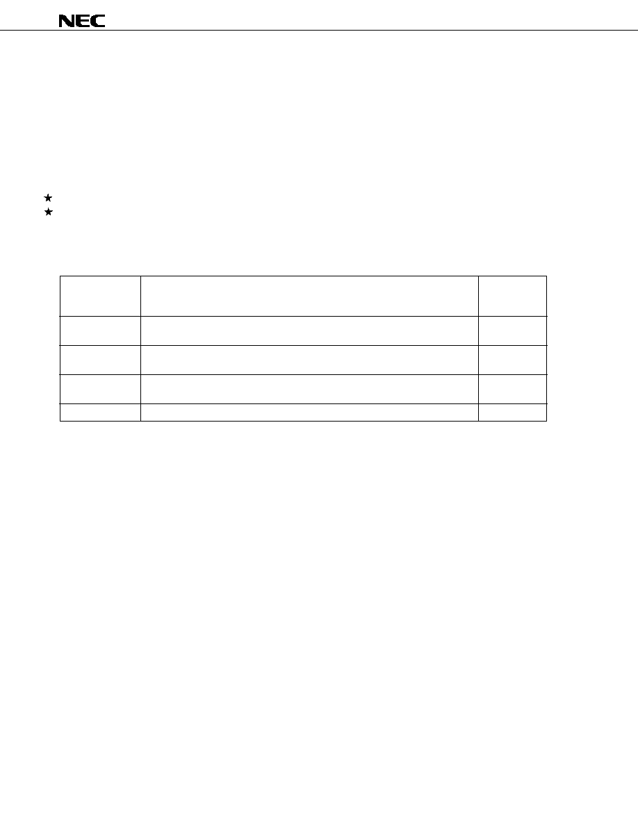
350
�
PD17704, 17705, 17707, 17708, 17709
26. RECOMMENDED SOLDERING CONDITIONS
Solder the
�
PD17709 under the following recommended conditions.
For the details of the recommended soldering conditions, refer to "Semiconductor Device Mounting Technology
Manual" (C10535E).
For the soldering method and conditions other than those recommended, consult NEC.
Table 26-1. Soldering Conditions of Surface Mount Type
�
PD17704GC-xxx-3B9: 80-pin plastic QFP (14
�
14 mm, 0.65 mm pitch)
�
PD17705GC-xxx-3B9: 80-pin plastic QFP (14
�
14 mm, 0.65 mm pitch)
�
PD17707GC-xxx-3B9: 80-pin plastic QFP (14
�
14 mm, 0.65 mm pitch)
�
PD17708GC-xxx-3B9: 80-pin plastic QFP (14
�
14 mm, 0.65 mm pitch)
�
PD17709GC-xxx-3B9: 80-pin plastic QFP (14
�
14 mm, 0.65 mm pitch)
Symbol of
Soldering Method
Soldering Condition
Recommended
Condition
Infrared reflow
Package peak temperature: 235
�
C, Time: 30 seconds MAX. (210
�
C MIN.)
IR35-00-2
Number of times: 2 MAX.
VPS
Package peak temperature: 215
�
C, Time: 40 seconds MAX. (200
�
C MIN.)
VP15-00-2
Number of times: 2 MAX.
Wave soldering
Soldering bath temperature: 260
�
C MAX., Time: 10 seconds MAX., Number of times: 1,
WS60-00-1
Preheating temperature: 120
�
C MAX. (package surface temperature)
Partial heating
Pin temperature: 300
�
C MAX., Time: 3 seconds MAX. (per side of device)
--
Caution Do not use two or more soldering methods in combination (except partial heating method).
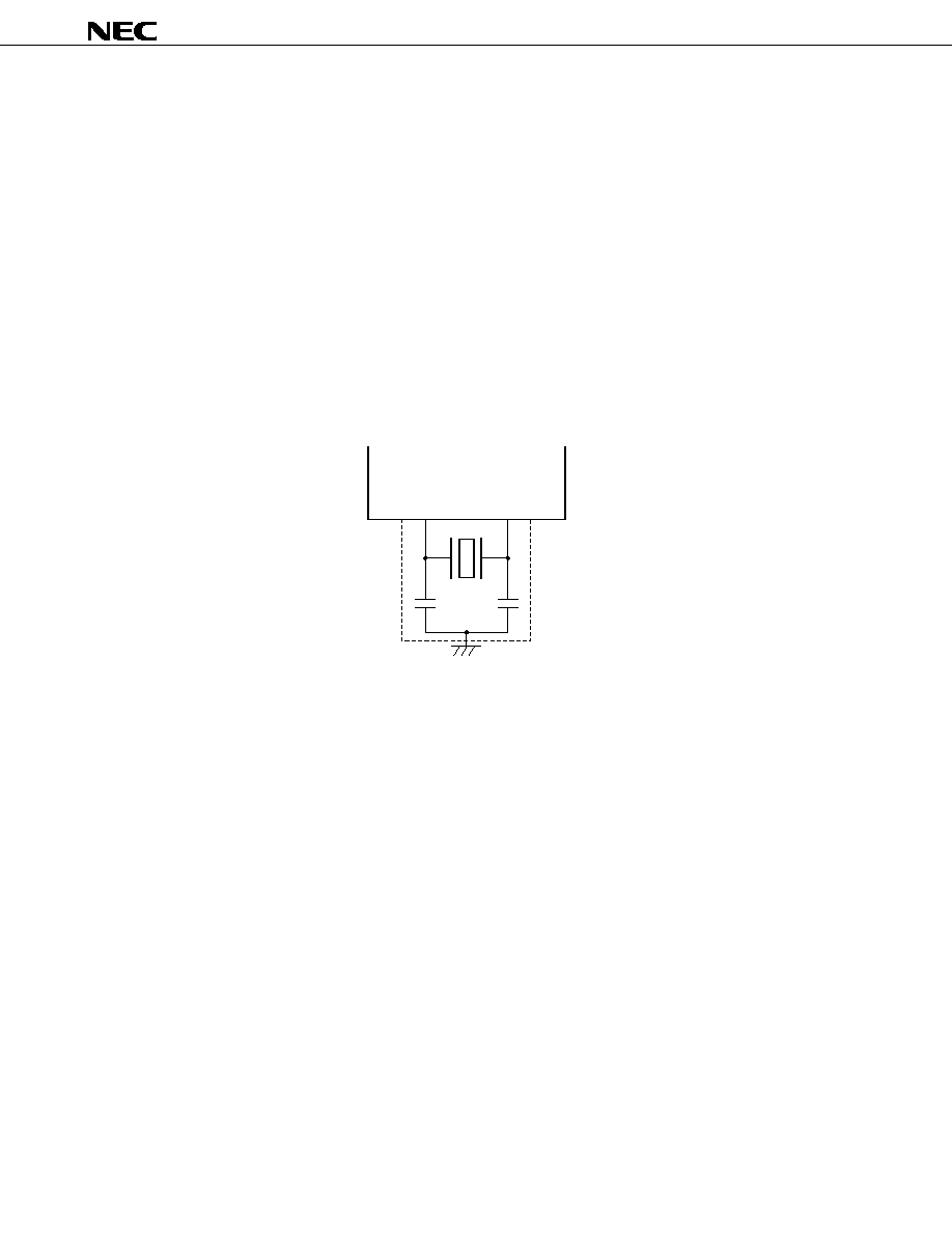
351
�
PD17704, 17705, 17707, 17708, 17709
APPENDIX A. CAUTIONS ON CONNECTING CRYSTAL RESONATOR
When using the system clock oscillation circuit, wire the portion enclosed by the dotted line in the figure below as
follows to prevent adverse influence from wiring capacity.
�
Keep the wiring length as short as possible.
�
If capacitances C1 and C2 are too high, the oscillation start characteristics may be degraded or current consumption
may increase.
�
Generally, connect a trimmer capacitor for adjusting the oscillation frequency to the X
IN
pin. Depending on the
crystal resonator to be used, however, the oscillation stability differs. Therefore, evaluate the crystal resonator
actually used.
�
The crystal oscillation frequency cannot be accurately adjusted when an emulation probe is connected to the
X
OUT
and X
IN
pin, because of the capacitance of the probe. Adjust the frequency while measuring the VCO
oscillation frequency.
PD17709
4.5-MHz crystal resonator
C1
C2
X
OUT
X
IN
�
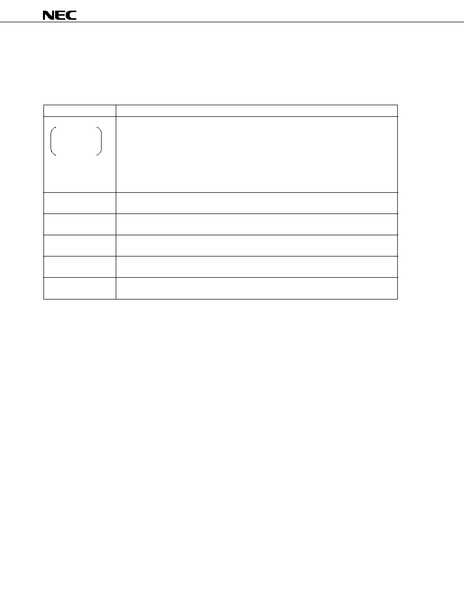
352
�
PD17704, 17705, 17707, 17708, 17709
APPENDIX B. DEVELOPMENT TOOLS
The following development tools are available for development of programs for the
�
PD17709.
Hardware
Name
Outline
IE-17K, IE-17K-ET, and EMU-17K are in-circuit emulators that can be used with any model in the 17K
series.
IE-17K and IE-17K-ET are connected to a host machine, which is PC-9800 series or IBM PC/AT
TM
,
with RS-232C. EMU-17K is mounted to the expansion slot of a host machine, PC-9800 series.
By using these in-circuit emulators with a system evaluation board (SE board) corresponding to each
model, these emulators operate dedicated to the model. When man-machine interface software
SIMPLEHOST
TM
is used, a more sophisticated debugging environment can be created.
EMU-17K also has a function to allow you to check the contents of the data memory real-time.
SE-17709 is an SE board for the
�
PD17709 subseries. This board can be used alone to evaluate a
system, or in combination with an in-circuit emulator for debugging.
EP-17K80GC is an emulation probe for the
�
PD17709 subseries. By using this probe with EV-
9200GC-80
Note 3
, the SE board and target system are connected.
EV-9200GC-80 is a conversion socket for 80-pin plastic QFP (14
�
14 mm). It is used to connect EP-
17K80GC and target system.
PG-1500 is a PROM programmer supporting
�
PD17P709. It can program
�
PD17P709 when connected
with PG-1500 adapter PA-17KDZ and programmer adapter PA-17P709GC.
PA-17P709GC is an adapter to program
�
PD17P709. It is used with PG-1500.
Notes 1. Low-price model: external power supply type
2. This is a product of I.C Corp. For details, consult I.C Corp. ((03) 3447-3793).
3. One EV-9200GC-80 is supplied with the EP-17K80GC. Five EV-9200GC-80 are also available as a set.
Remark
Third party PROM programmers AF-9703, AF-9704, AF-9705, and AF-9706 are available from Ando
Electric Co., Ltd. Use these programmers with programmer adapter PA-17P709GC. For details, consult
Ando Electric Co., Ltd. ((03) 3733-1163).
In-circuit emulator
IE-17K
IE-17K-ET
Note 1
EMU-17K
Note 2
SE board
(SE-17709)
Emulation probe
(EP-17K80GC)
Conversion socket
(EV-9200GC-80
Note 3
)
PROM programmer
(PG-1500)
Programmer adapter
(PA-17P709GC)
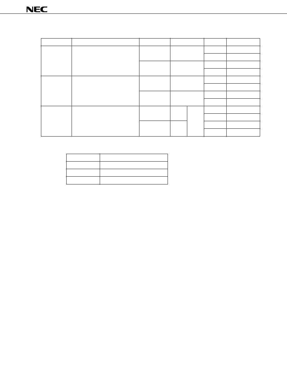
353
�
PD17704, 17705, 17707, 17708, 17709
Software
Name
Outline
Host Machine
OS
Media
Parts Number
17K series
PC-9800 series
MS-DOS
TM
5" 2HD
�
S5A10AS17K
assembler
3.5" 2HD
�
S5A13AS17K
(AS17K)
IBM PC/AT
PC DOS
TM
5" 2HC
�
S7B10AS17K
3.5" 2HC
�
S7B13AS17K
Device file
PC-9800 series
MS-DOS
5" 2HD
�
S5A10AS17707
(AS17707)
3.5" 2HD
�
S5A13AS17707
IBM PC/AT
PC DOS
5" 2HC
�
S7B10AS17707
3.5" 2HC
�
S7B13AS17707
Support
PC-9800 series
MS-DOS Windows
5" 2HD
�
S5A10IE17K
software
3.5" 2HD
�
S5A13IE17K
(
SIMPLEHOST)
IBM PC/AT
PC DOS
5" 2HC
�
S7B10IE17K
3.5" 2HC
�
S7B13IE17K
Remark
The version of the supported OS is as follows:
OS
Version
MS-DOS
Ver.3.30 ~ Ver.5.00A
Note
PC DOS
Ver.3.1~Ver.5.0
Note
Windows
Ver.3.0~Ver.3.1
Note
MS-DOS Ver. 5.00/5.00A and PC DOS Ver. 5.0
have a task swap function, but this function
cannot be used with this software.
AS17K is an assembler that can be
commonly used with 17K series.
To develop programs for the
�
PD17709,
this AS17K and a device file (AS17707)
are used in combination.
AS17707 is a device file for the
�
PD17709 subseries.
It is used with the assembler common
to the 17K series (AS17K).
SIMPLEHOST is man-machine
interface software that runs on
Windows
TM
when a program is
developed by using an in-circuit
emulator and personal computer.

354
�
PD17704, 17705, 17707, 17708, 17709
NOTES FOR CMOS DEVICES
1
PRECAUTION AGAINST ESD FOR SEMICONDUCTORS
Note: Strong electric field, when exposed to a MOS device, can cause destruction
of the gate oxide and ultimately degrade the device operation. Steps must
be taken to stop generation of static electricity as much as possible, and
quickly dissipate it once, when it has occurred. Environmental control must
be adequate. When it is dry, humidifier should be used. It is recommended
to avoid using insulators that easily build static electricity. Semiconductor
devices must be stored and transported in an anti-static container, static
shielding bag or conductive material. All test and measurement tools
including work bench and floor should be grounded. The operator should
be grounded using wrist strap. Semiconductor devices must not be touched
with bare hands. Similar precautions need to be taken for PW boards with
semiconductor devices on it.
2
HANDLING OF UNUSED INPUT PINS FOR CMOS
Note: No connection for CMOS device inputs can be cause of malfunction. If no
connection is provided to the input pins, it is possible that an internal input
level may be generated due to noise, etc., hence causing malfunction. CMOS
device behave differently than Bipolar or NMOS devices. Input levels of
CMOS devices must be fixed high or low by using a pull-up or pull-down
circuitry. Each unused pin should be connected to V
DD
or GND with a
resistor, if it is considered to have a possibility of being an output pin. All
handling related to the unused pins must be judged device by device and
related specifications governing the devices.
3
STATUS BEFORE INITIALIZATION OF MOS DEVICES
Note: Power-on does not necessarily define initial status of MOS device. Produc-
tion process of MOS does not define the initial operation status of the device.
Immediately after the power source is turned ON, the devices with reset
function have not yet been initialized. Hence, power-on does not guarantee
out-pin levels, I/O settings or contents of registers. Device is not initialized
until the reset signal is received. Reset operation must be executed imme-
diately after power-on for devices having reset function.

355
�
PD17704, 17705, 17707, 17708, 17709
NEC Electronics Inc. (U.S.)
Santa Clara, California
Tel: 800-366-9782
Fax: 800-729-9288
NEC Electronics (Germany) GmbH
Duesseldorf, Germany
Tel: 0211-65 03 02
Fax: 0211-65 03 490
NEC Electronics (UK) Ltd.
Milton Keynes, UK
Tel: 01908-691-133
Fax: 01908-670-290
NEC Electronics Italiana s.r.1.
Milano, Italy
Tel: 02-66 75 41
Fax: 02-66 75 42 99
NEC Electronics Hong Kong Ltd.
Hong Kong
Tel: 2886-9318
Fax: 2886-9022/9044
NEC Electronics Hong Kong Ltd.
Seoul Branch
Seoul, Korea
Tel: 02-528-0303
Fax: 02-528-4411
NEC Electronics Singapore Pte. Ltd.
United Square, Singapore 1130
Tel: 253-8311
Fax: 250-3583
NEC Electronics Taiwan Ltd.
Taipei, Taiwan
Tel: 02-719-2377
Fax: 02-719-5951
NEC do Brasil S.A.
Sao Paulo-SP, Brasil
Tel: 011-889-1680
Fax: 011-889-1689
NEC Electronics (Germany) GmbH
Benelux Office
Eindhoven, The Netherlands
Tel: 040-2445845
Fax: 040-2444580
NEC Electronics (France) S.A.
Velizy-Villacoublay, France
Tel: 01-30-67 58 00
Fax: 01-30-67 58 99
NEC Electronics (France) S.A.
Spain Office
Madrid, Spain
Tel: 01-504-2787
Fax: 01-504-2860
NEC Electronics (Germany) GmbH
Scandinavia Office
Taeby, Sweden
Tel: 08-63 80 820
Fax: 08-63 80 388
Regional Information
Some information contained in this document may vary from country to country. Before using any NEC
product in your application, please contact the NEC office in your country to obtain a list of authorized
representatives and distributors. They will verify:
� Device availability
� Ordering information
� Product release schedule
� Availability of related technical literature
� Development environment specifications (for example, specifications for third-party tools and
components, host computers, power plugs, AC supply voltages, and so forth)
� Network requirements
In addition, trademarks, registered trademarks, export restrictions, and other legal issues may also vary
from country to country.
J96. 8

2
�
PD17704, 17705, 17707, 17708, 17709
The export of this product from Japan is regulated by the Japanese government. To export this product may be prohibited
without governmental license, the need for which must be judged by the customer. The export or re-export of this product
from a country other than Japan may also be prohibited without a license from that country. Please call an NEC sales
representative.
SIMPLEHOST is a trademark of NEC Corporation.
MS-DOS and Windows are trademarks of Microsoft Corporation.
PC/AT and PC DOS are trademarks of IBM Corporation.
Purchase of NEC I
2
C components conveys a license under the Philips I
2
C Patent Rights to use these
components in an I
2
C system, provided that the system conforms to the I
2
C Standard Specification as defined
by Philips.
No part of this document may be copied or reproduced in any form or by any means without the prior written
consent of NEC Corporation. NEC Corporation assumes no responsibility for any errors which may appear in
this document.
NEC Corporation does not assume any liability for infringement of patents, copyrights or other intellectual property
rights of third parties by or arising from use of a device described herein or any other liability arising from use
of such device. No license, either express, implied or otherwise, is granted under any patents, copyrights or other
intellectual property rights of NEC Corporation or others.
While NEC Corporation has been making continuous effort to enhance the reliability of its semiconductor devices,
the possibility of defects cannot be eliminated entirely. To minimize risks of damage or injury to persons or
property arising from a defect in an NEC semiconductor device, customers must incorporate sufficient safety
measures in its design, such as redundancy, fire-containment, and anti-failure features.
NEC devices are classified into the following three quality grades:
"Standard", "Special", and "Specific". The Specific quality grade applies only to devices developed based on a
customer designated "quality assurance program" for a specific application. The recommended applications of
a device depend on its quality grade, as indicated below. Customers must check the quality grade of each device
before using it in a particular application.
Standard: Computers, office equipment, communications equipment, test and measurement equipment,
audio and visual equipment, home electronic appliances, machine tools, personal electronic
equipment and industrial robots
Special:
Transportation equipment (automobiles, trains, ships, etc.), traffic control systems, anti-disaster
systems, anti-crime systems, safety equipment and medical equipment (not specifically designed
for life support)
Specific:
Aircrafts, aerospace equipment, submersible repeaters, nuclear reactor control systems, life
support systems or medical equipment for life support, etc.
The quality grade of NEC devices is "Standard" unless otherwise specified in NEC's Data Sheets or Data Books.
If customers intend to use NEC devices for applications other than those specified for Standard quality grade,
they should contact an NEC sales representative in advance.
Anti-radioactive design is not implemented in this product.
M4 96.5