The information in this document is subject to change without notice. Before using this document, please
confirm that this is the latest version.
Not all devices/types available in every country. Please check with local NEC representative for
availability and additional information.
MOS INTEGRATED CIRCUIT
µ
µ
µ
µ
PD30121
V
R
4121
TM
64-/32-BIT MICROPROCESSOR
Document No. U14691EJ1V0DS00 (1st edition)
Date Published June 2000 N CP(K)
Printed in Japan
DATA SHEET
2000
©
DESCRIPTION
The
µ
PD30121 (V
R
4121) is one of NEC's V
R
Series
TM
RISC (Reduced Instruction Set Computer) microprocessors
and is a high-performance 64-/32-bit microprocessor employing the MIPS
TM
RISC architecture.
The V
R
4121 uses the high-performance, super power-saving V
R
4120
TM
as the CPU core, and has many peripheral
functions such as a DMA controller, software modem interface, serial interface, keyboard interface, IrDA interface,
touch panel interface, real-time clock, A/D converter, and D/A converter. Configured with these functions, the
V
R
4121 is suitable for high-speed battery-driven portable information systems. The external memory bus width can
be selected from 32 bits and 16 bits, realizing high-speed data transfer.
Detailed function descriptions are provided in the following user's manual. Be sure to read it before
designing.
∑
V
R
4121 User's Manual (U13569E)
FEATURES
∑ Employs 64-bit MIPS architecture
∑ Conforms to MIPS III instruction set (deleting FPU,
LL, LLD, SC, and SCD instructions)
∑ Memory controller (ROM, EDO-type DRAM,
synchronous DRAM (SDRAM), synchronous ROM
(SROM), and flash memory supported)
∑ Optimized 6-stage pipeline
∑ Keyboard interface and touch panel interface
∑ Supports MIPS16 instruction set
∑ 4-channel DMA controller
∑ Supports high-speed product-sum operation
instructions
∑ Serial interface (NS16550 compatible)
∑ IrDA interface for infrared communication
∑ Supports four types of operating modes, enabling
more effective power-consumption management
∑ Software modem interface
∑ A/D and D/A converters to support digital voice I/O
∑ Supports ISA bus subset
∑ Internal maximum operating frequency: 131/168 MHz
∑ On-chip clock generator
∑ Address space physical: 32 bits
virtual:
40 bits
Integrates 32 double entry TLBs
∑ Power supply voltage: V
DD
2 = 2.5 V (internal), V
DD
3 =
3.3 V (external) (131 MHz model)
∑ Package: 224-pin fine-pitch FBGA
∑ High-capacity instruction/data separated cache
memories
Instruction:
16 Kbytes
Data:
8 Kbytes
APPLICATIONS
∑
Battery-driven portable information systems
∑
Embedded controllers, etc.
ORDERING INFORMATION
Part Number
Package
Internal Maximum Operating Frequency
µ
PD30121F1-131-GA1
224-pin plastic FBGA (16
◊
16)
131 MHz
µ
PD30121F1-168-GA1
224-pin plastic FBGA (16
◊
16)
168 MHz

Data Sheet U14691EJ1V0DS00
5
µ
µ
µ
µ
PD30121
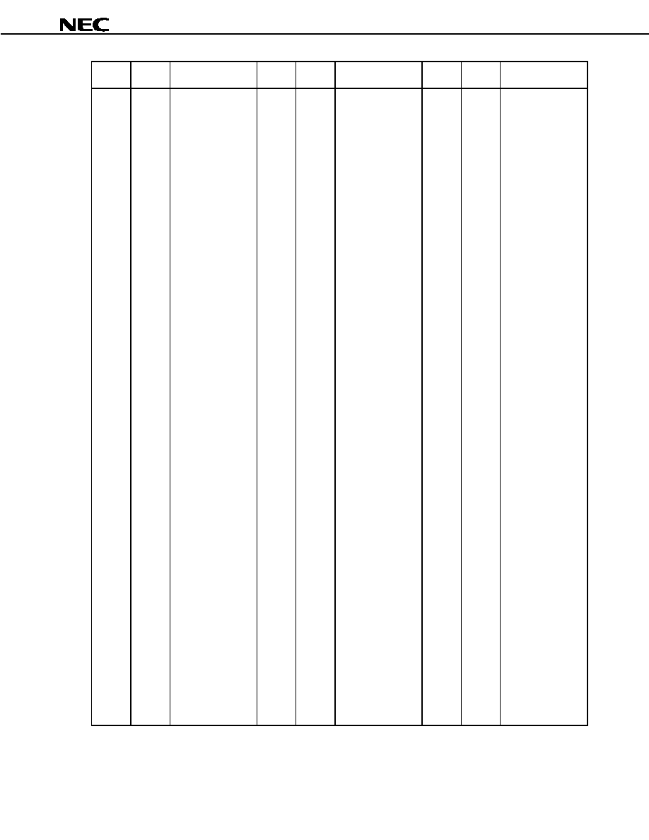
PIN IDENTIFICATION
ADD (0:25):
Address Bus
LCDCS#:
LCD Chip Select
ADIN (0:2):
General Purpose Input for A/D
LCDRDY:
LCD Ready
AFERST#:
AFE Reset
LEDOUT#:
LED Output
AGND:
GND for A/D
MEMCS16#:
Memory Chip Select 16
AUDIOIN:
Audio Input
MEMR#:
Memory Read
AUDIOOUT:
Audio Output
MEMW#:
Memory Write
AV
DD
:
V
DD
for A/D
MIPS16EN:
MIPS16 Enable
BATTINH:
Battery Inhibit
MPOWER:
Main Power
BATTINT#:
Battery Interrupt Request
MRAS(0:3)#:
DRAM Row Address Strobe
BUSCLK:
System Bus Clock
MUTE:
Mute
CGND:
GND for Oscillator
OFFHOOK:
Off Hook
CKE:
Clock Enable
OPD#:
Output Power Down
CLKSEL (0:2):
Clock Select
PIUGND:
GND for Touch Panel Interface
CLKX1:
Clock X1
PIUV
DD
:
V
DD
for Touch Panel Interface
CLKX2:
Clock X2
POWER:
Power Switch
CTS#:
Clear to Send
POWERON:
Power On State
CV
DD
:
V
DD
for Oscillator
RD#:
Read
DATA (0:31):
Data Bus
ROMCS(0:3)#:
ROM Chip Select
DBUS32:
Data Bus 32
RSTOUT:
System Bus Reset Output
DCD#:
Data Carrier Detect
RSTSW#:
Reset Switch
DCTS#:
Debug Serial Clear to Send
RTCRST#:
Real-time Clock Reset
DDIN:
Debug Serial Data Input
RTCX1:
Real-time Clock X1
DDOUT:
Debug Serial Data Output
RTCX2:
Real-time Clock X2
DGND:
GND for D/A
RTS#:
Request to Send
DRTS#:
Debug Serial Request to Send
RxD:
Receive Data
DSR#:
Data Set Ready
SCAS#:
DTR#:
Data Terminal Ready
Column Address Strobe for
SDRAM/SROM
DV
DD
:
V
DD
for D/A
SCLK:
SDRAM/SROM Clock
FIRCLK:
FIR Clock
SDI:
HSP Serial Data Input
FIRDIN#:
FIR Data Input
SDO:
HSP Serial Data Output
FS:
Frame Synchronization
SEL:
IrDA Module Select
GND2, GND3:
Ground
SHB#:
System Hi-Byte Enable
GNDP, GNDPD:
Ground for PLL
SMODE (1:2):
SDRAM Mode
GPIO (0:49):
General Purpose I/O
SPOWER:
SDRAM Power Control
HC0:
Hardware Control 0
SRAS#:
HLDACK#:
Hold Acknowledge
Row Address Strobe for
SDRAM/SROM
HLDRQ#:
Hold Request
SYSDIR:
System Bus Buffer Direction
HSPMCLK:
HSP Codec Master Clock
TELCON:
Telephone Control
HSPSCLK:
HSP Codec Serial Clock
TPX (0:1):
Touch Panel X I/O
ILCSENSE:
Input Loop Current Sensing
TPY (0:1):
Touch Panel Y I/O
IOCHRDY:
I/O Channel Ready
TxD:
Transmit Data
IOCS16#:
I/O Chip Select 16
UCAS#:
Upper Column Address Strobe
IOR#:
I/O Read
ULCAS#:
Lower Byte of Upper Column
IOW#:
I/O Write
Address Strobe
IRDIN:
IrDA Data Input
UUCAS#:
Upper Byte of Upper Column
IRDOUT#:
IrDA Data Output
Address Strobe
IRING:
Input Ring
V
DD
2, V
DD
3:
Power Supply Voltage
KPORT (0:7):
Key Code Data Input
V
DD
P, V
DD
PD:
V
DD
for PLL
KSCAN (0:11):
Key Scan Line
WR#:
Write
LCAS#:
Lower Column Address Strobe
ZWS#:
Zero Wait State
Remark # indicates active low.