Document Outline
- COVER
- Features
- Ordering Information
- Pin Configurations
- Block Diagram
- Electrical Specifications
- JTAG Specification
- Package Drawing

The mark shows major revised points.
The information in this document is subject to change without notice. Before using this document, please
confirm that this is the latest version.
Not all products and/or types are available in every country. Please check with an NEC Electronics
sales representative for availability and additional information.
MOS INTEGRATED CIRCUIT
µ
µ
µ
µ
PD44164082, 44164182, 44164362
18M-BIT DDRII SRAM
2-WORD BURST OPERATION
Document No. M15821EJ7V2DS00 (7th edition)
Date Published August 2004 NS CP(K)
Printed in Japan
DATA SHEET
2001
Description
The
µ
PD44164082 is a 2,097,152-word by 8-bit, the
µ
PD44164182 is a 1,048,576-word by 18-bit and the
µ
PD44164362 is a 524,288-word by 36-bit synchronous double data rate static RAM fabricated with advanced CMOS
technology using full CMOS six-transistor memory cell.
The
µ
PD44164082,
µ
PD44164182 and
µ
PD44164362 integrates unique synchronous peripheral circuitry and a
burst counter. All input registers controlled by an input clock pair (K and /K) are latched on the positive edge of K and
/K.
These products are suitable for application which require synchronous operation, high speed, low voltage, high
density and wide bit configuration.
These products are packaged in 165-pin PLASTIC BGA.
Features
∑ 1.8 ± 0.1 V power supply and HSTL I/O
∑ DLL circuitry for wide output data valid window and future frequency scaling
∑ Pipelined double data rate operation
∑ Common data input/output bus
∑ Two-tick burst for low DDR transaction size
∑ Two input clocks (K and /K) for precise DDR timing at clock rising edges only
∑ Two output clocks (C and /C) for precise flight time
and clock skew matching-clock and data delivered together to receiving device
∑ Internally self-timed write control
∑ Clock-stop capability with
µ
s restart
∑ User programmable impedance output
∑ Fast clock cycle time : 4.0 ns (250 MHz), 5.0 ns (200 MHz), 6.0 ns (167 MHz)
∑ Simple control logic for easy depth expansion
∑ JTAG boundary scan

2
Data Sheet M15821EJ7V2DS
µ
µ
µ
µ
PD44164082, 44164182, 44164362
Ordering Information
Part number
Cycle
Clock
Organization
Core Supply
I/O
Package
Time Frequency
(word
x
bit) Voltage Interface
ns MHz
V
µ
PD44164082F5-E40-EQ1
4.0
250
2 M x 8-bit
1.8 ± 0.1
HSTL
165-pin PLASTIC
µ
PD44164082F5-E50-EQ1
5.0
200
BGA (13 x 15)
µ
PD44164082F5-E60-EQ1 6.0 167
µ
PD44164182F5-E40-EQ1
4.0
250
1 M x 18-bit
µ
PD44164182F5-E50-EQ1 5.0 200
µ
PD44164182F5-E60-EQ1 6.0 167
µ
PD44164362F5-E50-EQ1
5.0
200
512 K x 36-bit
µ
PD44164362F5-E60-EQ1 6.0 167
3
Data Sheet M15821EJ7V2DS
µ
µ
µ
µ
PD44164082, 44164182, 44164362
Pin Configurations
/
◊◊◊ indicates active low signal.
165-pin PLASTIC BGA (13 x 15)
(Top View)
[
µ
µ
µ
µ
PD44164082F5-EQ1]
1 2 3 4 5 6 7 8 9 10
11
A /CQ V
SS
A R,
/W
/NW1
/K NC /LD A V
SS
CQ
B
NC NC NC A NC K /NW0 A NC NC
DQ3
C NC NC NC V
SS
A A A V
SS
NC NC NC
D NC NC NC V
SS
V
SS
V
SS
V
SS
V
SS
NC NC NC
E NC NC DQ4 V
DD
Q V
SS
V
SS
V
SS
V
DD
Q NC NC DQ2
F NC NC NC V
DD
Q V
DD
V
SS
V
DD
V
DD
Q NC NC NC
G NC NC DQ5 V
DD
Q V
DD
V
SS
V
DD
V
DD
Q NC NC NC
H /DLL V
REF
V
DD
Q V
DD
Q V
DD
V
SS
V
DD
V
DD
Q V
DD
Q V
REF
ZQ
J NC NC NC V
DD
Q V
DD
V
SS
V
DD
V
DD
Q NC DQ1 NC
K NC NC NC V
DD
Q V
DD
V
SS
V
DD
V
DD
Q NC NC NC
L NC DQ6 NC V
DD
Q V
SS
V
SS
V
SS
V
DD
Q NC NC DQ0
M NC NC NC V
SS
V
SS
V
SS
V
SS
V
SS
NC NC NC
N NC NC NC V
SS
A A A V
SS
NC NC NC
P
NC
NC
DQ7
A A C A A NC
NC
NC
R
TDO
TCK A A A /C A A A
TMS
TDI
A
: Address inputs
TMS
: IEEE 1149.1 Test input
DQ0 to DQ7
: Data inputs / outputs
TDI
: IEEE 1149.1 Test input
/LD
: Synchronous load
TCK
: IEEE 1149.1 Clock input
R, /W
: Read Write input
TDO
: IEEE 1149.1 Test output
/NW0, /NW1
: Nibble Write data select
V
REF
: HSTL input reference input
K, /K
: Input clock
V
DD
: Power Supply
C, /C
: Output clock
V
DD
Q
: Power Supply
CQ, /CQ
: Echo clock
V
SS
:
Ground
ZQ
: Output impedance matching
NC
: No connection
/DLL
: DLL disable
Remark Refer to Package Drawing for the index mark.

4
Data Sheet M15821EJ7V2DS
µ
µ
µ
µ
PD44164082, 44164182, 44164362
165-pin PLASTIC BGA (13 x 15)
(Top View)
[
µ
µ
µ
µ
PD44164182F5-EQ1]
1 2 3 4 5 6 7 8 9 10
11
A /CQ V
SS
A R,
/W
/BW1
/K NC /LD A V
SS
CQ
B
NC
DQ9
NC A NC K /BW0 A NC NC
DQ8
C NC NC NC V
SS
A A0 A V
SS
NC DQ7 NC
D NC NC DQ10 V
SS
V
SS
V
SS
V
SS
V
SS
NC NC NC
E NC NC DQ11 V
DD
Q V
SS
V
SS
V
SS
V
DD
Q NC NC DQ6
F NC DQ12 NC V
DD
Q V
DD
V
SS
V
DD
V
DD
Q NC NC DQ5
G NC NC DQ13 V
DD
Q V
DD
V
SS
V
DD
V
DD
Q NC NC NC
H /DLL V
REF
V
DD
Q V
DD
Q V
DD
V
SS
V
DD
V
DD
Q V
DD
Q V
REF
ZQ
J NC NC NC V
DD
Q V
DD
V
SS
V
DD
V
DD
Q NC DQ4 NC
K NC NC DQ14 V
DD
Q V
DD
V
SS
V
DD
V
DD
Q NC NC DQ3
L NC DQ15 NC V
DD
Q V
SS
V
SS
V
SS
V
DD
Q NC NC DQ2
M NC NC NC V
SS
V
SS
V
SS
V
SS
V
SS
NC DQ1 NC
N NC NC DQ16 V
SS
A A A V
SS
NC NC NC
P
NC
NC
DQ17
A A C A A NC
NC
DQ0
R
TDO
TCK A A A /C A A A
TMS
TDI
A0, A
: Address inputs
TMS
: IEEE 1149.1 Test input
DQ0 to DQ17
: Data inputs / outputs
TDI
: IEEE 1149.1 Test input
/LD
: Synchronous load
TCK
: IEEE 1149.1 Clock input
R, /W
: Read Write input
TDO
: IEEE 1149.1 Test output
/BW0, /BW1
: Byte Write data select
V
REF
: HSTL input reference input
K, /K
: Input clock
V
DD
: Power Supply
C, /C
: Output clock
V
DD
Q
: Power Supply
CQ, /CQ
: Echo clock
V
SS
:
Ground
ZQ
: Output impedance matching
NC
: No connection
/DLL
: DLL disable
Remark Refer to Package Drawing for the index mark.
5
Data Sheet M15821EJ7V2DS
µ
µ
µ
µ
PD44164082, 44164182, 44164362
165-pin PLASTIC BGA (13 x 15)
(Top View)
[
µ
µ
µ
µ
PD44164362F5-EQ1]
1 2 3 4 5 6 7 8 9 10
11
A /CQ V
SS
NC R,
/W
/BW2 /K /BW1
/LD A V
SS
CQ
B
NC DQ27
DQ18 A /BW3 K /BW0 A NC NC DQ8
C NC NC DQ28 V
SS
A A0 A V
SS
NC DQ17
DQ7
D NC DQ29 DQ19 V
SS
V
SS
V
SS
V
SS
V
SS
NC NC DQ16
E NC NC DQ20 V
DD
Q V
SS
V
SS
V
SS
V
DD
Q NC DQ15 DQ6
F NC DQ30 DQ21 V
DD
Q V
DD
V
SS
V
DD
V
DD
Q NC NC DQ5
G NC DQ31 DQ22 V
DD
Q V
DD
V
SS
V
DD
V
DD
Q NC NC DQ14
H /DLL V
REF
V
DD
Q V
DD
Q V
DD
V
SS
V
DD
V
DD
Q V
DD
Q V
REF
ZQ
J NC NC DQ32 V
DD
Q V
DD
V
SS
V
DD
V
DD
Q NC DQ13 DQ4
K NC NC DQ23 V
DD
Q V
DD
V
SS
V
DD
V
DD
Q NC DQ12 DQ3
L NC DQ33 DQ24 V
DD
Q V
SS
V
SS
V
SS
V
DD
Q NC NC DQ2
M NC NC DQ34 V
SS
V
SS
V
SS
V
SS
V
SS
NC DQ11
DQ1
N NC DQ35 DQ25 V
SS
A A A V
SS
NC NC DQ10
P
NC
NC
DQ26
A A C A A NC
DQ9
DQ0
R
TDO
TCK A A A /C A A A
TMS
TDI
A0, A
: Address inputs
TMS
: IEEE 1149.1 Test input
DQ0 to DQ35
: Data inputs / outputs
TDI
: IEEE 1149.1 Test input
/LD
: Synchronous load
TCK
: IEEE 1149.1 Clock input
R, /W
: Read Write input
TDO
: IEEE 1149.1 Test output
/BW0 to /BW3
: Byte Write data select
V
REF
: HSTL input reference input
K, /K
: Input clock
V
DD
: Power Supply
C, /C
: Output clock
V
DD
Q
: Power Supply
CQ, /CQ
: Echo clock
V
SS
:
Ground
ZQ
: Output impedance matching
NC
: No connection
/DLL
: DLL disable
Remark Refer to Package Drawing for the index mark.

6
Data Sheet M15821EJ7V2DS
µ
µ
µ
µ
PD44164082, 44164182, 44164362
Pin Identification
Symbol Description
A0
A
Synchronous Address Inputs: These inputs are registered and must meet the setup and hold times around the
rising edge of K. Balls 3A, 10A, and 2A are reserved for the next higher-order address inputs on future devices.
All transactions operate on a burst of two words (one clock period of bus activity). A0 is used as the lowest
order address bit permitting a random starting address within the burst operation. These inputs are ignored
when device is deselected.
DQ0 to DQxx Synchronous Data IOs: Input data must meet setup and hold times around the rising edges of K and /K. Output
data is synchronized to the respective C and /C data clocks or to K and /K if C and /C are tied to HIGH.
x8 device uses DQ0 to DQ7.
x18 device uses DQ0 to DQ17.
x36 device uses DQ0 to DQ35.
/LD
Synchronous Load: This input is brought LOW when a bus cycle sequence is to be defined. This definition
includes address and read/write direction. All transactions operate on a burst of 2 data (one clock period of bus
activity).
R, /W
Synchronous Read/Write Input: When /LD is LOW, this input designates the access type (READ when R, /W is
HIGH, WRITE when R, /W is LOW) for the loaded address. R, /W must meet the setup and hold times around
the rising edge of K.
/BWx
/NWx
Synchronous Byte Writes (Nibble Writes on x8): When LOW these inputs cause their respective byte or nibble
to be registered and written during WRITE cycles. These signals must meet setup and hold times around the
rising edges of K and /K for each of the two rising edges comprising the WRITE cycle. See Pin Configurations
for signal to data relationships.
K, /K
Input Clock: This input clock pair registers address and control inputs on the rising edge of K, and registers data
on the rising edge of K and the rising edge of /K. /K is ideally 180 degrees out of phase with K. All synchronous
inputs must meet setup and hold times around the clock rising edges.
C, /C
Output Clock: This clock pair provides a user controlled means of tuning device output data. The rising edge of
/C is used as the output timing reference for first output data. The rising edge of C is used as the output
reference for second output data. Ideally, /C is 180 degrees out of phase with C. C and /C may be tied HIGH to
force the use of K and /K as the output reference clocks instead of having to provide C and /C clocks. If tied
HIGH, C and /C must remain HIGH and not be toggled during device operation.
CQ, /CQ
Synchronous Echo Clock Outputs. The rising edges of these outputs are tightly matched to the synchronous
data outputs and can be used as a data valid indication. These signals run freely and do not stop when Q
tristates.
ZQ
Output Impedance Matching Input: This input is used to tune the device outputs to the system data bus
impedance. DQ and CQ output impedance are set to 0.2 x RQ, where RQ is a resistor from this bump to
ground. This pin cannot be connected directly to GND or left unconnected. Also, in this product, there is no
function to minimize the output impedance by connecting ZQ directly to V
DD
Q.
/DLL
DLL Disable: When LOW, this input causes the DLL to be bypassed for stable low frequency operation.
TMS
TDI
IEEE 1149.1 Test Inputs: 1.8V I/O levels. These balls may be left Not Connected if the JTAG function is not
used in the circuit.
TCK
IEEE 1149.1 Clock Input: 1.8V I/O levels. This pin must be tied to V
SS
if the JTAG function is not used in the
circuit.
TDO
IEEE 1149.1 Test Output: 1.8V I/O level.
V
REF
HSTL Input Reference Voltage: Nominally V
DD
Q/2. Provides a reference voltage for the input buffers.
V
DD
Power Supply: 1.8V nominal. See DC Characteristics and Operating Conditions for range.
V
DD
Q
Power Supply: Isolated Output Buffer Supply. Nominally 1.5V. 1.8V is also permissible. See DC Characteristics
and Operating Conditions for range.
V
SS
Power Supply: Ground
NC
No Connect: These signals are internally connected and appear in the JTAG scan chain as the logic level
applied to the ball sites. These signals may be connected to ground to improve package heat dissipation.
7
Data Sheet M15821EJ7V2DS
µ
µ
µ
µ
PD44164082, 44164182, 44164362
Block Diagram
2 : 1
MUX
0
1
/A0'
A0'
/A0'
A0'
0
1
Input
Register
E
/K
R, /W
Input
Register
E
Write address
Register
E
K
R, /W
Register
E
Output control
Logic
/C
C
Address
Register
E
/LD
Address
A0''
A0'''
Compare
Output Buffer
ZQ
DQ
Output Enable
Register
C
Burst
Logic
D0
Q0
A0
CLK
A0'
WRITE Register
Memory
Array
WRITE Driver
Sense Amps
Output Register
A0'
CLK
K
E
A0'''
R
/W

8
Data Sheet M15821EJ7V2DS
µ
µ
µ
µ
PD44164082, 44164182, 44164362
Burst Sequence
Linear Burst Sequence Table
[
µ
µ
µ
µ
PD44164182,
µ
µ
µ
µ
PD44164362]
A0
A0
External Address
0
1
1st Internal Burst Address
1
0
Truth Table
Operation /LD
R,
/W
CLK
DQ
WRITE cycle
L
L
L
H
Data in
Load address, input write data on two
Input data
D(A1)
D(A2)
consecutive K and /K rising edge
Input clock
K(t+1)
/K(t+1)
READ cycle
L
H
L
H
Data out
Load address, read data on two
Output data
Q(A1)
Q(A2)
consecutive C and /C rising edge
Output clock
/C(t+1)
C(t+2)
NOP (No operation)
H
X
L
H
High-Z
STANDBY(Clock stopped)
X
X
Stopped
Previous state
Remarks 1. H : High level, L : Low level,
◊ : don't care, : rising edge.
2. Data inputs are registered at K and /K rising edges. Data outputs are delivered at C and /C rising edges
except if C and /C are HIGH then Data outputs are delivered at K and /K rising edges.
3. All control inputs in the truth table must meet setup/hold times around the rising edge (LOW to HIGH) of
K. All control inputs are registered during the rising edge of K.
4. This device contains circuitry that will ensure the outputs will be in high impedance during power-up.
5. Refer to state diagram and timing diagrams for clarification.
6. A1 refers to the address input during a WRITE or READ cycle. A2 refers to the next internal burst
address in accordance with the linear burst sequence.
7. It is recommended that K = /K = C = /C when clock is stopped. This is not essential but permits most
rapid restart by overcoming transmission line charging symmetrically.

9
Data Sheet M15821EJ7V2DS
µ
µ
µ
µ
PD44164082, 44164182, 44164362
Byte Write Operation
[
µ
µ
µ
µ
PD44164082]
Operation K
/K
/NW0
/NW1
Write DQ0 to DQ7
L
H
≠
0 0
≠
L
H
0
0
Write DQ0 to DQ3
L
H
≠
0 1
≠
L
H
0
1
Write DQ4 to DQ7
L
H
≠
1 0
≠
L
H
1
0
Write nothing
L
H
≠
1 1
≠
L
H
1
1
Remark H : High level, L : Low level,
: rising edge.
[
µ
µ
µ
µ
PD44164182]
Operation K
/K
/BW0
/BW1
Write DQ0 to DQ17
L
H
≠
0 0
≠
L
H
0
0
Write DQ0 to DQ8
L
H
≠
0 1
≠
L
H
0
1
Write DQ9 to DQ17
L
H
≠
1 0
≠
L
H
1
0
Write nothing
L
H
≠
1 1
≠
L
H
1
1
Remark H : High level, L : Low level,
: rising edge.
[
µ
µ
µ
µ
PD44164362]
Operation
K
/K /BW0 /BW1 /BW2 /BW3
Write DQ0 to DQ35
L
H
≠
0 0 0 0
≠
L
H
0 0 0 0
Write DQ0 to DQ8
L
H
≠
0 1 1 1
≠
L
H
0 1 1 1
Write DQ9 to DQ17
L
H
≠
1 0 1 1
≠
L
H
1 0 1 1
Write DQ18 to DQ26
L
H
≠
1 1 0 1
≠
L
H
1 1 0 1
Write DQ27 to DQ35
L
H
≠
1 1 1 0
≠
L
H
1 1 1 0
Write nothing
L
H
≠
1 1 1 1
≠
L
H
1 1 1 1
Remark H : High level, L : Low level,
: rising edge.

10
Data Sheet M15821EJ7V2DS
µ
µ
µ
µ
PD44164082, 44164182, 44164362
Bus Cycle State Diagram
READ DOUBLE
Count = Count + 2
WRITE DOUBLE
Count = Count + 2
Power UP
Write
NOP
Supply voltage provided
LOAD NEW
ADDRESS
Count = 0
NOP
Load, Count = 2
Read
Load, Count = 2
Load
NOP,
Count = 2
NOP,
Count = 2
Remarks 1. A0 is internally advanced in accordance with the burst order table.
Bus cycle is terminated after burst count = 2.
2.
State machine control timing sequence is controlled by K.

11
Data Sheet M15821EJ7V2DS
µ
µ
µ
µ
PD44164082, 44164182, 44164362
Electrical Specifications
Absolute Maximum Ratings
Parameter Symbol
Conditions
MIN.
TYP.
MAX.
Unit
Supply voltage
V
DD
≠0.5
+2.9
V
Output supply voltage
V
DD
Q
≠0.5
V
DD
V
Input voltage
V
IN
≠0.5
V
DD
+ 0.5 (2.9 V MAX.)
V
Input / Output voltage
V
I/O
≠0.5
V
DD
Q
+ 0.5 (2.9 V MAX.)
V
Operating ambient temperature
T
A
0
70
∞C
Storage temperature
T
stg
≠55
+125
∞C
Caution Exposing the device to stress above those listed in Absolute Maximum Ratings could cause
permanent damage. The device is not meant to be operated under conditions outside the limits
described in the operational section of this specification. Exposure to Absolute Maximum Rating
conditions for extended periods may affect device reliability.
Recommended DC Operating Conditions (T
A
= 0 to 70
∞
∞
∞
∞C)
Parameter Symbol
Conditions
MIN.
TYP.
MAX.
Unit
Note
Supply voltage
V
DD
1.7
1.9
V
Output supply voltage
V
DD
Q
1.4
V
DD
V
1
High level input voltage
V
IH (DC)
V
REF
+ 0.1
V
DD
Q
+ 0.3
V
1, 2
Low level input voltage
V
IL (DC)
≠0.3
V
REF
≠ 0.1
V
1, 2
Clock input voltage
V
IN
≠0.3
V
DD
Q
+ 0.3
V
1, 2
Reference voltage
V
REF
0.68
0.95
V
Notes 1. During normal operation, V
DD
Q must not exceed V
DD
.
2. Power-up: V
IH
V
DD
Q + 0.3 V and V
DD
1.7 V and V
DD
Q
1.4 V for t 200 ms
Recommended AC Operating Conditions (T
A
= 0 to 70
∞
∞
∞
∞C)
Parameter Symbol
Conditions
MIN.
TYP.
MAX.
Unit
Note
High level input voltage
V
IH (AC)
V
REF
+ 0.2
≠
V
1
Low level input voltage
V
IL (AC)
≠
V
REF
≠ 0.2
V
1
Note 1. Overshoot: V
IH (AC)
V
DD
+ 0.7 V for t
TKHKH/2
Undershoot:
V
IL (AC)
≠ 0.5 V for t TKHKH/2
Control input signals may not have pulse widths less than TKHKL (MIN.) or operate at cycle rates less than
TKHKH (MIN.).

12
Data Sheet M15821EJ7V2DS
µ
µ
µ
µ
PD44164082, 44164182, 44164362
DC Characteristics (T
A
= 0 to 70∞C, V
DD
= 1.8 ± 0.1 V)
Parameter Symbol
Test
condition MIN.
TYP.
MAX.
Unit
Note
x8,
x18
x36
Input leakage current
I
LI
≠2
≠
+2
µ
A
I/O leakage current
I
LO
≠2
≠
+2
µ
A
Operating supply current
I
DD
V
IN
V
IL
or V
IN
V
IH
, ≠E40
650
≠
mA
(Read Write cycle)
I
I/O
= 0 mA
≠E50
550
650
Cycle = MAX.
≠E60
480
570
Standby supply current
I
SB1
V
IN
V
IL
or V
IN
V
IH
, ≠E40
320
≠
mA
(NOP)
I
I/O
= 0 mA
≠E50
270
Cycle = MAX.
≠E60
250
High level output voltage
V
OH(Low)
|I
OH
|
0.1 mA
V
DD
Q
≠ 0.2
≠
V
DD
Q V
3,
4
V
OH
Note1
V
DD
Q/2 ≠ 0.12
≠
V
DD
Q/2 + 0.12
V
3, 4
Low level output voltage
V
OL(Low)
I
OL
0.1 mA
V
SS
≠ 0.2 V
3,
4
V
OL
Note2
V
DD
Q/2 ≠ 0.12
≠
V
DD
Q/2 + 0.12
V
3, 4
Notes 1. Outputs are impedance-controlled. | I
OH
| = (V
DD
Q/2)/(RQ/5) for values of 175
RQ 350 .
2. Outputs are impedance-controlled. I
OL
= (V
DD
Q/2)/(RQ/5) for values of 175
RQ 350 .
3. AC load current is higher than the shown DC values.
4. HSTL outputs meet JEDEC HSTL Class I and Class II standards.
Capacitance (T
A
= 25
∞
∞
∞
∞C, f = 1MHz)
Parameter Symbol
Test
conditions
MIN.
TYP.
MAX.
Unit
Input capacitance
C
IN
V
IN
= 0 V
4
5
pF
Input / Output capacitance
C
I/O
V
I/O
= 0 V
6
7
pF
Clock Input capacitance
C
clk
V
clk
= 0 V
5
6
pF
Remark These parameters are periodically sampled and not 100% tested.

13
Data Sheet M15821EJ7V2DS
µ
µ
µ
µ
PD44164082, 44164182, 44164362
AC Characteristics (T
A
= 0 to 70
∞
∞
∞
∞C, V
DD
= 1.8 ± 0.1 V)
AC Test Conditions
Input waveform (Rise / Fall time
0.3 ns)
0.75 V
0.75 V
Test Points
1.25 V
0.25 V
Output
waveform
V
DD
Q / 2
V
DD
Q / 2
Test Points
Output load condition
Figure 1. External load at test
V
DD
Q / 2
0.75 V
50
Z
O
= 50
250
SRAM
V
REF
ZQ
14
Data Sheet M15821EJ7V2DS
µ
µ
µ
µ
PD44164082, 44164182, 44164362
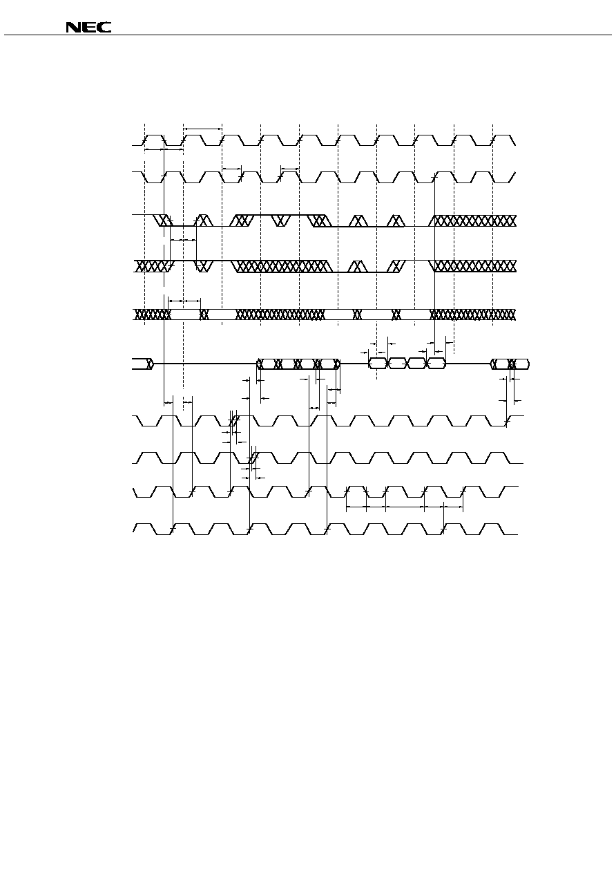
Read and Write Cycle
Parameter Symbol
-E40 -E50 -E60
Unit Note
(250 MHz)
(200 MHz)
(167 MHz)
MIN. MAX. MIN. MAX. MIN. MAX.
Clock
Average Clock cycle time (K, /K, C, /C) TKHKH
4.0 8.4 5.0 8.4 6.0 8.4
ns 1
Clock phase jitter (K, /K, C, /C)
TKC var
≠ 0.2 ≠ 0.2 ≠ 0.2
ns 2
Clock HIGH time (K, /K, C, /C)
TKHKL
1.6 ≠ 2.0 ≠ 2.4 ≠
ns
Clock LOW time (K, /K, C, /C)
TKLKH
1.6 ≠ 2.0 ≠ 2.4 ≠
ns
Clock to /clock (K
/K., C/C.) TKH
/KH
1.8 ≠ 2.2 ≠ 2.7 ≠
ns
Clock to /clock (/K
K., /CC.) T
/KHKH
1.8 ≠ 2.2 ≠ 2.7 ≠
ns
Clock to data clock 200 to 250 MHz
TKHCH
0 1.8 ≠ ≠ ≠ ≠
ns
(K
C., /K/C.)
167 to 200 MHz
0 2.3 0 2.3 ≠ ≠
133 to 167 MHz
0 2.8 0 2.8 0 2.8
< 133 MHz
0 3.55 0 3.55 0 3.55
DLL lock time (K, C)
TKC lock
1,024 ≠ 1,024 ≠ 1,024 ≠
Cycle
3
K static to DLL reset
TKC reset
30 ≠ 30 ≠ 30 ≠
ns
Output Times
C, /C HIGH to output valid
TCHQV
≠ 0.45 ≠ 0.45 ≠ 0.5
ns
C, /C HIGH to output hold
TCHQX
≠0.45 ≠ ≠0.45 ≠ ≠0.5 ≠ ns
C, /C HIGH to echo clock valid
TCHCQV
≠ 0.45 ≠ 0.45 ≠ 0.5
ns
C, /C HIGH to echo clock hold
TCHCQX
≠0.45 ≠ ≠0.45 ≠ ≠0.5 ≠ ns
CQ, /CQ HIGH to output valid
TCQHQV
≠ 0.3 ≠ 0.35 ≠ 0.4
ns 4
CQ, /CQ HIGH to output hold
TCQHQX
≠0.3 ≠ ≠0.35 ≠ ≠0.4 ≠ ns 4
C HIGH to output High-Z
TCHQZ
≠ 0.45 ≠ 0.45 ≠ 0.5
ns
C HIGH to output Low-Z
TCHQX1
≠0.45 ≠ ≠0.45 ≠ ≠0.5 ≠ ns
Setup Times
Address valid to K rising edge
TAVKH
0.5 ≠ 0.6 ≠ 0.7 ≠
ns 5
Synchronous load input (/LD),
TIVKH
0.5 ≠ 0.6 ≠ 0.7 ≠
ns 5
read write input (R, /W) valid to
K rising edge
Data inputs and write data select
TDVKH
0.35 ≠ 0.4 ≠ 0.5 ≠
ns 5
inputs (/BWx, /NWx) valid to
K, /K rising edge
Hold Times
K rising edge to address hold
TKHAX
0.5 ≠ 0.6 ≠ 0.7 ≠
ns 5
K rising edge to
TKHIX
0.5 ≠ 0.6 ≠ 0.7 ≠
ns 5
synchronous load input (/LD),
read write input (R, /W) hold
K, /K rising edge to data inputs and
TKHDX
0.35 ≠ 0.4 ≠ 0.5 ≠
ns 5
write data select inputs (/BWx, /NWx)
hold

15
Data Sheet M15821EJ7V2DS
µ
µ
µ
µ
PD44164082, 44164182, 44164362
Notes 1. The device will operate at clock frequencies slower than TKHKH(MAX.).
2. Clock phase jitter is the variance from clock rising edge to the next expected clock rising edge.
3. V
DD
slew rate must be less than 0.1 V DC per 50 ns for DLL lock retention.
DLL lock time begins once V
DD
and input clock are stable.
It is recommended that the device is kept inactive during these cycles.
4. Echo clock is very tightly controlled to data valid / data hold. By design, there is a
± 0.1 ns variation from
echo clock to data. The data sheet parameters reflect tester guardbands and test setup variations.
5. This is a synchronous device. All addresses, data and control lines must meet the specified setup
and hold times for all latching clock edges.
Remarks 1. This parameter is sampled.
2. Test conditions as specified with the output loading as shown in AC Test Conditions
unless otherwise noted.
3. Control input signals may not be operated with pulse widths less than TKHKL (MIN.).
4. If C, /C are tied HIGH, K, /K become the references for C, /C timing parameters.
5.
V
DD
Q is 1.5 V DC.
16
Data Sheet M15821EJ7V2DS
µ
µ
µ
µ
PD44164082, 44164182, 44164362
Read and Write Timing
TKHKH
TKHAX
Q01
Q11
K
/LD
Address
DQ
Q02
/K
2
4
6
8
10
1
3
5
7
9
R, /W
A0
A1
A2
Qx2
Q12
TKH/KH
T/KHKH
CQ
/CQ
C
/C
TKHCH
TCHQX1
TCHQV
TCHQV
TCHQX
TCHQZ
TKHKL TKLKH TKHKH TKH/KH
D21
D31
D22
D32
TDVKH
TKHDX
TDVKH
TKHDX
NOP
READ
(burst of 2)
READ
(burst of 2)
NOP
NOP
WRITE
(burst of 2)
WRITE
(burst of 2)
TKHKL
TIVKH
TKLKH
TKHIX
TKLKH
TCHCQV
TCHCQV
TCHCQX
TCHCQX
TCQHQX
TCQHQV
READ
(burst of 2)
A3
A4
TCHQX
Q41
Q42
T/KHKH
TAVKH
TKHCH
Remarks 1. Q01 refers to output from address A0.
Q02 refers to output from the next internal burst address following A0, etc.
2. Outputs are disable (high impedance) one clock cycle after a NOP.
3. The second NOP cycle is not necessary for correct device operation;
however, at high clock frequencies it may be required to prevent bus contention.

17
Data Sheet M15821EJ7V2DS
µ
µ
µ
µ
PD44164082, 44164182, 44164362
JTAG Specification
These products support a limited set of JTAG functions as in IEEE standard 1149.1.
Test Access Port (TAP) Pins
Pin name
Pin assignments
Description
TCK
2R
Test Clock Input. All input are captured on the rising edge of TCK and all outputs
propagate from the falling edge of TCK.
TMS
10R
Test Mode Select. This is the command input for the TAP controller state machine.
TDI
11R
Test Data Input. This is the input side of the serial registers placed between TDI and
TDO. The register placed between TDI and TDO is determined by the state of the TAP
controller state machine and the instruction that is currently loaded in the TAP instruction.
TDO
1R
Test Data Output. Output changes in response to the falling edge of TCK. This is the
output side of the serial registers placed between TDI and TDO.
Remark The device does not have TRST (TAP reset). The Test-Logic Reset state is entered while TMS is held high
for five rising edges of TCK. The TAP controller state is also reset on the SRAM POWER-UP.
JTAG DC Characteristics (T
A
= 0 to 70∞C, V
DD
= 1.8 ± 0.1 V, unless otherwise noted)
Parameter Symbol Conditions MIN.
TYP.
MAX.
Unit
Note
JTAG Input leakage current
I
LI
0
V
V
IN
V
DD
≠5.0
≠
+5.0
µ
A
JTAG I/O leakage current
I
LO
0
V
V
IN
V
DD
Q, ≠5.0
≠
+5.0
µ
A
Outputs
disabled
JTAG input high voltage
V
IH
1.3
≠ V
DD
+ 0.3
V
JTAG input low voltage
V
IL
≠0.3
≠
+0.5 V
JTAG output high voltage
V
OH1
|
I
OHC
| = 100
µ
A 1.6
≠
≠
V
V
OH2
|
I
OHT
| = 2 mA
1.4
≠
≠
V
JTAG output low voltage
V
OL1
I
OLC
= 100
µ
A ≠
≠
0.2
V
V
OL2
I
OLT
= 2 mA
≠
≠
0.4
V

18
Data Sheet M15821EJ7V2DS
µ
µ
µ
µ
PD44164082, 44164182, 44164362
JTAG AC Test Conditions
Input waveform (Rise / Fall time
1 ns)
0.9 V
0.9 V
Test Points
1.8 V
0 V
Output
waveform
0.9 V
0.9 V
Test Points
Output
load
Figure 2. External load at test
TDO
Z
O
= 50
V
TT
= 0.9 V
20 pF
50

19
Data Sheet M15821EJ7V2DS
µ
µ
µ
µ
PD44164082, 44164182, 44164362
JTAG AC Characteristics (T
A
= 0 to 70
∞
∞
∞
∞C)
Parameter Symbol Conditions
MIN.
TYP.
MAX.
Unit
Note
Clock
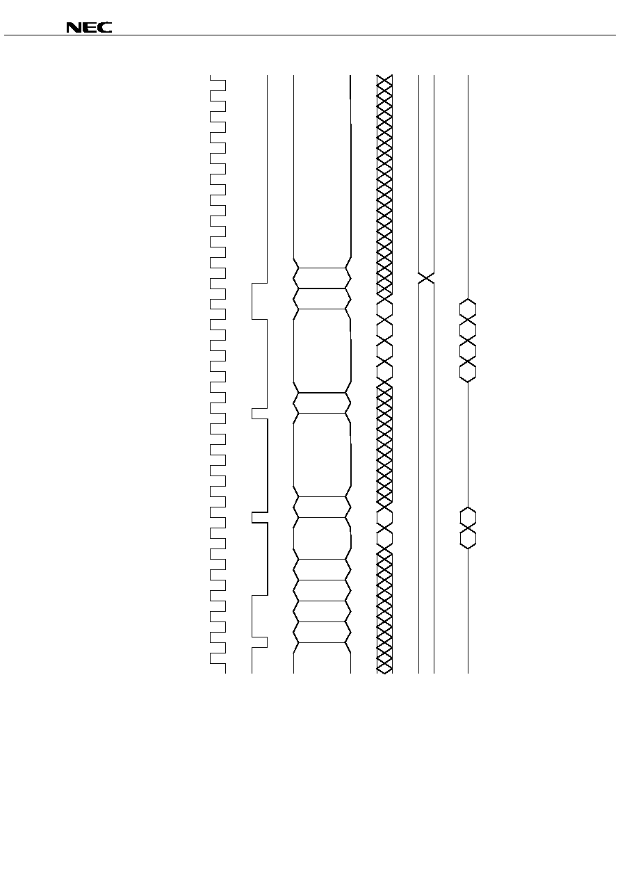
Clock cycle time
t
THTH
100 ≠
≠ ns
Clock frequency
f
TF
≠ ≠ 10 MHz
Clock high time
t
THTL
40
≠
≠ ns
Clock low time
t
TLTH
40
≠
≠ ns
Output
time
TCK low to TDO unknown
t
TLOX
0 ≠ ≠
ns
TCK low to TDO valid
t
TLOV
≠
≠
20 ns
TDI valid to TCK high
t
DVTH
10
≠
≠ ns
TCK high to TDI invalid
t
THDX
10
≠
≠ ns
Setup
time
TMS setup time
t
MVTH
10
≠
≠ ns
Capture setup time
t
CS
10 ≠ ≠ ns
Hold
time
TMS hold time
t
THMX
10
≠
≠ ns
Capture hold time
t
CH
10 ≠
≠ ns
JTAG Timing Diagram
t
THTH
t
TLOV
t
TLTH
t
THTL
t
MVTH
t
THDX
t
DVTH
t
THMX
TCK
TMS
TDI
TDO
t
TLOX

20
Data Sheet M15821EJ7V2DS
µ
µ
µ
µ
PD44164082, 44164182, 44164362
Scan Register Definition (1)
Register name
Description
Instruction register
The instruction register holds the instructions that are executed by the TAP controller when it is
moved into the run-test/idle or the various data register state. The register can be loaded when it is
placed between the TDI and TDO pins. The instruction register is automatically preloaded with the
IDCODE instruction at power-up whenever the controller is placed in test-logic-reset state.
Bypass register
The bypass register is a single bit register that can be placed between TDI and TDO. It allows serial
test data to be passed through the RAMs TAP to another device in the scan chain with as little delay
as possible.
ID register
The ID Register is a 32 bit register that is loaded with a device and vendor specific 32 bit code when
the controller is put in capture-DR state with the IDCODE command loaded in the instruction register.
The register is then placed between the TDI and TDO pins when the controller is moved into shift-DR
state.
Boundary register
The boundary register, under the control of the TAP controller, is loaded with the contents of the
RAMs I/O ring when the controller is in capture-DR state and then is placed between the TDI and
TDO pins when the controller is moved to shift-DR state. Several TAP instructions can be used to
activate the boundary register.
The Scan Exit Order tables describe which device bump connects to each boundary register
location. The first column defines the bit's position in the boundary register. The second column is
the name of the input or I/O at the bump and the third column is the bump number.
Scan Register Definition (2)
Register name
Bit size
Unit
Instruction register
3
bit
Bypass register
1
bit
ID register
32
bit
Boundary register
107
bit
ID Register Definition
Part number
Organization ID [31:28] vendor revision no.
ID [27:12] part no.
ID [11:1] vendor ID no.
ID [0] fix bit
µ
PD44164082
2M x 8
XXXX
0000 0000 0001 0010
00000010000
1
µ
PD44164182
1M x 18
XXXX
0000 0000 0001 0011
00000010000
1
µ
PD44164362
512K x 36
XXXX
0000 0000 0001 0100
00000010000
1

21
Data Sheet M15821EJ7V2DS
µ
µ
µ
µ
PD44164082, 44164182, 44164362
SCAN Exit Order
Bit
Signal name
Bump
Bit
Signal name
Bump
Bit
Signal name
Bump
no. x8 x18 x36 ID no. x8 x18 x36 ID no. x8 x18 x36 ID
1 /C 6R
37
NC
NC
NC
10D
73 NC NC NC 2C
2 C 6P
38
NC
NC
NC
9E
74
DQ4
DQ11
DQ20
3E
3 A 6N
39
NC
DQ7 DQ17 10C
75 NC
NC
DQ29
2D
4 A 7P
40
NC
NC
DQ16 11D
76 NC
NC
NC
2E
5 A 7N
41
NC
NC
NC
9C
77 NC
NC
NC
1E
6 A 7R
42
NC
NC
NC
9D
78 NC
DQ12
DQ30
2F
7 A 8R
43
DQ3 DQ8
DQ8
11B
79 NC
NC
DQ21
3F
8 A 8P
44
NC
NC
DQ7
11C
80 NC
NC
NC
1G
9 A 9R
45
NC
NC
NC
9B
81 NC
NC
NC 1F
10 NC DQ0
DQ0
11P 46 NC NC NC 10B 82 DQ5 DQ13
DQ22 3G
11 NC NC DQ9
10P 47 CQ 11A 83 NC NC DQ31 2G
12 NC NC NC 10N 48
≠
Internal
84 NC NC NC 1J
13 NC NC NC 9P 49 A 9A 85 NC NC NC 2J
14 NC DQ1
DQ11 10M 50
A
8B 86 NC DQ14
DQ23 3K
15 NC NC
DQ10 11N 51
A
7C 87 NC NC DQ32 3J
16
NC
NC
NC 9M 52 A A0 A0 6C 88 NC NC NC 2K
17 NC NC NC 9N 53 /LD 8A 89 NC NC NC 1K
18 DQ0 DQ2 DQ2
11L 54 NC NC /BW1
7A
90 DQ6 DQ15 DQ33 2L
19 NC NC DQ1
11M 55 /NW0 /BW0 /BW0
7B 91 NC NC DQ24 3L
20 NC NC NC 9L 56 K 6B 92 NC NC NC 1M
21 NC NC NC 10L 57 /K 6A 93 NC NC NC 1L
22 NC DQ3
DQ3
11K 58 NC NC /BW3
5B 94 NC DQ16
DQ25 3N
23 NC NC
DQ12
10K 59 /NW1 /BW1 /BW2
5A 95 NC NC DQ34 3M
24 NC NC NC 9J 60 R,
/W
4A 96 NC NC NC 1N
25 NC NC NC 9K 61 A 5C 97 NC NC NC 2M
26 DQ1 DQ4
DQ13
10J 62
A
4B 98 DQ7 DQ17 DQ26 3P
27
NC
NC
DQ4
11J 63 A A NC 3A 99 NC NC
DQ35
2N
28 ZQ 11H 64 /DLL
1H 100 NC NC NC 2P
29 NC NC NC 10G 65 /CQ 1A 101 NC NC NC 1P
30 NC NC NC 9G 66 NC DQ9 DQ27
2B 102
A
3R
31 NC DQ5
DQ5
11F 67 NC NC DQ18
3B 103
A
4R
32 NC NC
DQ14 11G 68 NC NC NC 1C 104
A
4P
33 NC NC NC 9F 69 NC NC NC 1B 105
A
5P
34 NC NC NC 10F 70 NC DQ10 DQ19
3D 106
A
5N
35 DQ2 DQ6 DQ6
11E 71 NC NC DQ28
3C 107
A
5R
36
NC
NC
DQ15
10E
72
NC
NC
NC
1D

22
Data Sheet M15821EJ7V2DS
µ
µ
µ
µ
PD44164082, 44164182, 44164362
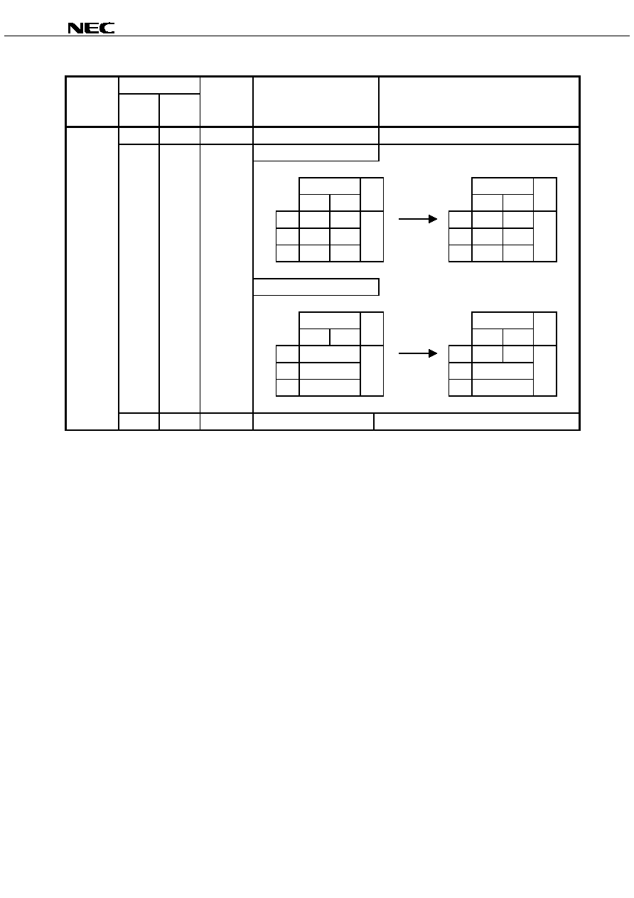
JTAG Instructions
Instructions Description
EXTEST
The EXTEST instruction allows circuitry external to the component package to be tested. Boundary-
scan register cells at output pins are used to apply test vectors, while those at input pins capture test
results. Typically, the first test vector to be applied using the EXTEST instruction will be shifted into the
boundary scan register using the PRELOAD instruction. Thus, during the update-IR state of EXTEST,
the output driver is turned on and the PRELOAD data is driven onto the output pins.
IDCODE
The IDCODE instruction causes the ID ROM to be loaded into the ID register when the controller is in
capture-DR mode and places the ID register between the TDI and TDO pins in shift-DR mode. The
IDCODE instruction is the default instruction loaded in at power up and any time the controller is placed
in the test-logic-reset state.
BYPASS
The BYPASS instruction is loaded in the instruction register when the bypass register is placed between
TDI and TDO. This occurs when the TAP controller is moved to the shift-DR state. This allows the
board level scan path to be shortened to facilitate testing of other devices in the scan path.
SAMPLE / PRELOAD SAMPLE / PRELOAD is a Standard 1149.1 mandatory public instruction. When the SAMPLE /
PRELOAD instruction is loaded in the instruction register, moving the TAP controller into the capture-DR
state loads the data in the RAMs input and DQ pins into the boundary scan register. Because the RAM
clock(s) are independent from the TAP clock (TCK) it is possible for the TAP to attempt to capture the
I/O ring contents while the input buffers are in transition (i.e., in a metastable state). Although allowing
the TAP to sample metastable input will not harm the device, repeatable results cannot be expected.
RAM input signals must be stabilized for long enough to meet the TAPs input data capture setup plus
hold time (t
CS
plus t
CH
). The RAMs clock inputs need not be paused for any other TAP operation except
capturing the I/O ring contents into the boundary scan register. Moving the controller to shift-DR state
then places the boundary scan register between the TDI and TDO pins.
SAMPLE-Z
If the SAMPLE-Z instruction is loaded in the instruction register, all RAM DQ pins are forced to an
inactive drive state (high impedance) and the boundary register is connected between TDI and TDO
when the TAP controller is moved to the shift-DR state.
JTAG Instruction Coding
IR2 IR1 IR0 Instruction Note
0 0 0 EXTEST
0 0 1 IDCODE
0 1 0 SAMPLE-Z 1
0 1 1 RESERVED
1
0
0
SAMPLE / PRELOAD
1 0 1 RESERVED
1 1 0 RESERVED
1 1 1 BYPASS
Note 1. TRISTATE all DQ pins and CAPTURE the pad values into a SERIAL SCAN LATCH.

23
Data Sheet M15821EJ7V2DS
µ
µ
µ
µ
PD44164082, 44164182, 44164362
TAP Controller State Diagram
Test-Logic-Reset
Run-Test / Idle
Select-DR-Scan
Capture-DR
Capture-IR
Shift-DR
Exit1-DR
Pause-DR
Exit2-DR
Update-DR
Update-IR
Exit2-IR
Pause-IR
Exit1-IR
Shift-IR
Select-IR-Scan
0
0
0
1
0
1
1
0
0
1
0
1
1
0
0
0
0
1
0
1
0
1
1
1
0
1
1
0
1
0
1
1
Disabling the Test Access Port
It is possible to use this device without utilizing the TAP. To disable the TAP Controller without interfering with normal
operation of the device, TCK must be tied to V
SS
to preclude mid level inputs.
TDI and TMS are designed so an undriven input will produce a response identical to the application of a logic 1, and
may be left unconnected. But they may also be tied to V
DD
through a 1 k
resistor.
TDO should be left unconnected.
24
Data S
heet
M1582
1EJ7V2DS
µ
µ
µ
µ
PD44164082, 44164182, 44164362
Test Logic Operation (Instruction Scan)
TCK
Controller
state
TDI
TMS
TDO
Test-Logic-Reset
Run-Test/Idle
Select-DR-Scan
Select-IR-Scan
Capture-IR
Shift-IR
Exit1-IR
Pause-IR
Exit2-IR
Shift-IR
Exit1-IR
Update-IR
Run-Test/Idle
IDCODE
Instruction
Register state
New Instruction
Output Inactive

25
Data S
heet
M1582
1EJ7V2DS
µ
µ
µ
µ
PD44164082, 44164182, 44164362
Test Logic (Data Scan)
Controller
state
TDI
TMS
TDO
Run-Test/Idle
Select-DR-Scan
Capture-DR
Shift-DR
Exit1-DR
Pause-DR
Exit2-DR
Shift-DR
Exit1-DR
Update-DR
Test-Logic-Reset
Instruction
Instruction
Register state
IDCODE
Run-Test/Idle
Select-DR-Scan
Select-IR-Scan
Output Inactive
TCK

26
Data Sheet M15821EJ7V2DS
µ
µ
µ
µ
PD44164082, 44164182, 44164362
Package Drawing
165-PIN PLASTIC BGA (13x15)
ITEM
DIMENSIONS
D
E
w
e
A
A1
A2
13.00
±
0.10
15.00
±
0.10
0.15
0.40
±
0.05
1.00
1.40
±
0.11
1.00
0.50
±
0.05
(UNIT:mm)
0.08
0.10
0.20
1.50
0.50
P165F5-100-EQ1
x
y
y1
ZD
ZE
b
A
11
10
9
8
7
6
5
4
3
2
1
INDEX MARK
ZE
ZD
B
S
w
B
E
S
w
A
D
S
y
S
A
A2
A1
e
y1
S
S
x
b
A B
M
R P M M L K J H G F E D C B A

27
Data Sheet M15821EJ7V2DS
µ
µ
µ
µ
PD44164082, 44164182, 44164362
Recommended Soldering Condition
Please consult with our sales offices for soldering conditions of these products.
Types of Surface Mount Devices
µ
PD44164082F5-EQ1: 165-pin PLASTIC BGA (13 x 15)
µ
PD44164182F5-EQ1: 165-pin PLASTIC BGA (13 x 15)
µ
PD44164362F5-EQ1: 165-pin PLASTIC BGA (13 x 15)
28
Data Sheet M15821EJ7V2DS
µ
µ
µ
µ
PD44164082, 44164182, 44164362
Revision History
Edition/ Page
Type
of Location
Description
Date This
Previous
revision
(Previous
edition
This edition)
edition
edition
7th edition/
Throughout Throughout
Deletion Ordering
Information
µ
PD44164362F5-E40-EQ1
Feb. 2004
p.12
p.12
Modification DC Characteristics I
DD
(MAX.)
MAX.
Unit
MAX.
Unit
x8, x18
x36
x8, x18
x36
-E40
600 TBD mA
-E40 650
-
mA
-E50
500 600
-E50 550 650
-E60
430 520
-E60 480 570
DC Characteristics I
SB1
(MAX.)
MAX.
Unit
MAX.
Unit
x8, x18
x36
x8, x18
x36
-E40
250 mA
-E40 320
- mA
-E50
210
-E50 270
-E60
190
-E60 250
p.26
p.26
Modification Package Drawing
Preliminary version
Standardized version

29
Data Sheet M15821EJ7V2DS
µ
µ
µ
µ
PD44164082, 44164182, 44164362
[MEMO]

30
Data Sheet M15821EJ7V2DS
µ
µ
µ
µ
PD44164082, 44164182, 44164362
[MEMO]

31
Data Sheet M15821EJ7V2DS
µ
µ
µ
µ
PD44164082, 44164182, 44164362
1
2
3
4
VOLTAGE APPLICATION WAVEFORM AT INPUT PIN
Waveform distortion due to input noise or a reflected wave may cause malfunction. If the input of the
CMOS device stays in the area between V
IL
(MAX) and V
IH
(MIN) due to noise, etc., the device may
malfunction. Take care to prevent chattering noise from entering the device when the input level is fixed,
and also in the transition period when the input level passes through the area between V
IL
(MAX) and
V
IH
(MIN).
HANDLING OF UNUSED INPUT PINS
Unconnected CMOS device inputs can be cause of malfunction. If an input pin is unconnected, it is
possible that an internal input level may be generated due to noise, etc., causing malfunction. CMOS
devices behave differently than Bipolar or NMOS devices. Input levels of CMOS devices must be fixed
high or low by using pull-up or pull-down circuitry. Each unused pin should be connected to V
DD
or GND
via a resistor if there is a possibility that it will be an output pin. All handling related to unused pins must
be judged separately for each device and according to related specifications governing the device.
PRECAUTION AGAINST ESD
A strong electric field, when exposed to a MOS device, can cause destruction of the gate oxide and
ultimately degrade the device operation. Steps must be taken to stop generation of static electricity as
much as possible, and quickly dissipate it when it has occurred. Environmental control must be
adequate. When it is dry, a humidifier should be used. It is recommended to avoid using insulators that
easily build up static electricity. Semiconductor devices must be stored and transported in an anti-static
container, static shielding bag or conductive material. All test and measurement tools including work
benches and floors should be grounded. The operator should be grounded using a wrist strap.
Semiconductor devices must not be touched with bare hands. Similar precautions need to be taken for
PW boards with mounted semiconductor devices.
STATUS BEFORE INITIALIZATION
Power-on does not necessarily define the initial status of a MOS device. Immediately after the power
source is turned ON, devices with reset functions have not yet been initialized. Hence, power-on does
not guarantee output pin levels, I/O settings or contents of registers. A device is not initialized until the
reset signal is received. A reset operation must be executed immediately after power-on for devices
with reset functions.
POWER ON/OFF SEQUENCE
In the case of a device that uses different power supplies for the internal operation and external
interface, as a rule, switch on the external power supply after switching on the internal power supply.
When switching the power supply off, as a rule, switch off the external power supply and then the
internal power supply. Use of the reverse power on/off sequences may result in the application of an
overvoltage to the internal elements of the device, causing malfunction and degradation of internal
elements due to the passage of an abnormal current.
The correct power on/off sequence must be judged separately for each device and according to related
specifications governing the device.
INPUT OF SIGNAL DURING POWER OFF STATE
Do not input signals or an I/O pull-up power supply while the device is not powered. The current
injection that results from input of such a signal or I/O pull-up power supply may cause malfunction and
the abnormal current that passes in the device at this time may cause degradation of internal elements.
Input of signals during the power off state must be judged separately for each device and according to
related specifications governing the device.
NOTES FOR CMOS DEVICES
5
6

µ
µ
µ
µ
PD44164082, 44164182, 44164362
The information in this document is current as of August, 2004. The information is subject to
change without notice. For actual design-in, refer to the latest publications of NEC Electronics data
sheets or data books, etc., for the most up-to-date specifications of NEC Electronics products. Not
all products and/or types are available in every country. Please check with an NEC Electronics sales
representative for availability and additional information.
No part of this document may be copied or reproduced in any form or by any means without the prior
written consent of NEC Electronics. NEC Electronics assumes no responsibility for any errors that may
appear in this document.
NEC Electronics does not assume any liability for infringement of patents, copyrights or other intellectual
property rights of third parties by or arising from the use of NEC Electronics products listed in this document
or any other liability arising from the use of such products. No license, express, implied or otherwise, is
granted under any patents, copyrights or other intellectual property rights of NEC Electronics or others.
Descriptions of circuits, software and other related information in this document are provided for illustrative
purposes in semiconductor product operation and application examples. The incorporation of these
circuits, software and information in the design of a customer's equipment shall be done under the full
responsibility of the customer. NEC Electronics assumes no responsibility for any losses incurred by
customers or third parties arising from the use of these circuits, software and information.
While NEC Electronics endeavors to enhance the quality, reliability and safety of NEC Electronics products,
customers agree and acknowledge that the possibility of defects thereof cannot be eliminated entirely. To
minimize risks of damage to property or injury (including death) to persons arising from defects in NEC
Electronics products, customers must incorporate sufficient safety measures in their design, such as
redundancy, fire-containment and anti-failure features.
NEC Electronics products are classified into the following three quality grades: "Standard", "Special" and
"Specific".
The "Specific" quality grade applies only to NEC Electronics products developed based on a customer-
designated "quality assurance program" for a specific application. The recommended applications of an NEC
Electronics product depend on its quality grade, as indicated below. Customers must check the quality grade of
each NEC Electronics product before using it in a particular application.
The quality grade of NEC Electronics products is "Standard" unless otherwise expressly specified in NEC
Electronics data sheets or data books, etc. If customers wish to use NEC Electronics products in applications
not intended by NEC Electronics, they must contact an NEC Electronics sales representative in advance to
determine NEC Electronics' willingness to support a given application.
(Note)
∑
∑
∑
∑
∑
∑
M8E 02. 11-1
(1)
(2)
"NEC Electronics" as used in this statement means NEC Electronics Corporation and also includes its
majority-owned subsidiaries.
"NEC Electronics products" means any product developed or manufactured by or for NEC Electronics (as
defined above).
Computers, office equipment, communications equipment, test and measurement equipment, audio
and visual equipment, home electronic appliances, machine tools, personal electronic equipment
and industrial robots.
Transportation equipment (automobiles, trains, ships, etc.), traffic control systems, anti-disaster
systems, anti-crime systems, safety equipment and medical equipment (not specifically designed
for life support).
Aircraft, aerospace equipment, submersible repeaters, nuclear reactor control systems, life
support systems and medical equipment for life support, etc.
"Standard":
"Special":
"Specific":