The information in this document is subject to change without notice. Before using this document, please
confirm that this is the latest version.
Not all products and/or types are available in every country. Please check with NEC Electronics sales
representative for availability and additional information.
MOS INTEGRATED CIRCUIT
µ
PD44321182, 44321362
32M-BIT ZEROSB
TM
SRAM
PIPELINED OPERATION
Document No. M16024EJ5V0DS00 (5th edition)
Date Published April 2005 NS CP(K)
Printed in Japan
DATA SHEET
The mark shows major revised points.
2002, 2005
Description
The
µ
PD44321182 is a 2,097,152-word by 18-bit and the
µ
PD44321362 is a 1,048,576-word by 36-bit ZEROSB
static RAM fabricated with advanced CMOS technology using full CMOS six-transistor memory cell.
The
µ
PD44321182 and
µ
PD44321362 are optimized to eliminate dead cycles for read to write, or write to read
transitions. These ZEROSB static RAMs integrate unique synchronous peripheral circuitry, 2-bit burst counter and
output buffer as well as SRAM core. All input registers are controlled by a positive edge of the single clock input
(CLK).
The
µ
PD44321182 and
µ
PD44321362 are suitable for applications which require synchronous operation, high speed,
low voltage, high density and wide bit configuration, such as buffer memory.
ZZ has to be set LOW at the normal operation. When ZZ is set HIGH, the SRAM enters Power Down State ("Sleep").
In the "Sleep" state, the SRAM internal state is preserved. When ZZ is set LOW again, the SRAM resumes normal
operation.
The
µ
PD44321182 and
µ
PD44321362 are packaged in 100-pin PLASTIC LQFP with a 1.4 mm package thickness for
high density and low capacitive loading.
Features
∑ Low voltage core supply : V
DD
= 3.3 ± 0.165 V / 2.5 ± 0.125 V
∑ Synchronous operation
∑ 100 percent bus utilization
∑ Internally self-timed write control
∑ Burst read / write : Interleaved burst and linear burst sequence
∑ Fully registered inputs and outputs for pipelined operation
∑ All registers triggered off positive clock edge
∑ 3.3V or 2.5V LVTTL Compatible : All inputs and outputs
∑ Fast clock access time : 3.2 ns (200 MHz)
∑ Asynchronous output enable : /G
∑ Burst sequence selectable : MODE
∑ Sleep mode : ZZ (ZZ = Open or Low : Normal operation)
∑ Separate byte write enable : /BW1 to /BW4 (
µ
PD44321362)
/BW1 and /BW2 (
µ
PD44321182)
∑ Three chip enables for easy depth expansion
∑ Common I/O using three state outputs

4
Data Sheet M16024EJ5V0DS
µ
PD44321182, 44321362
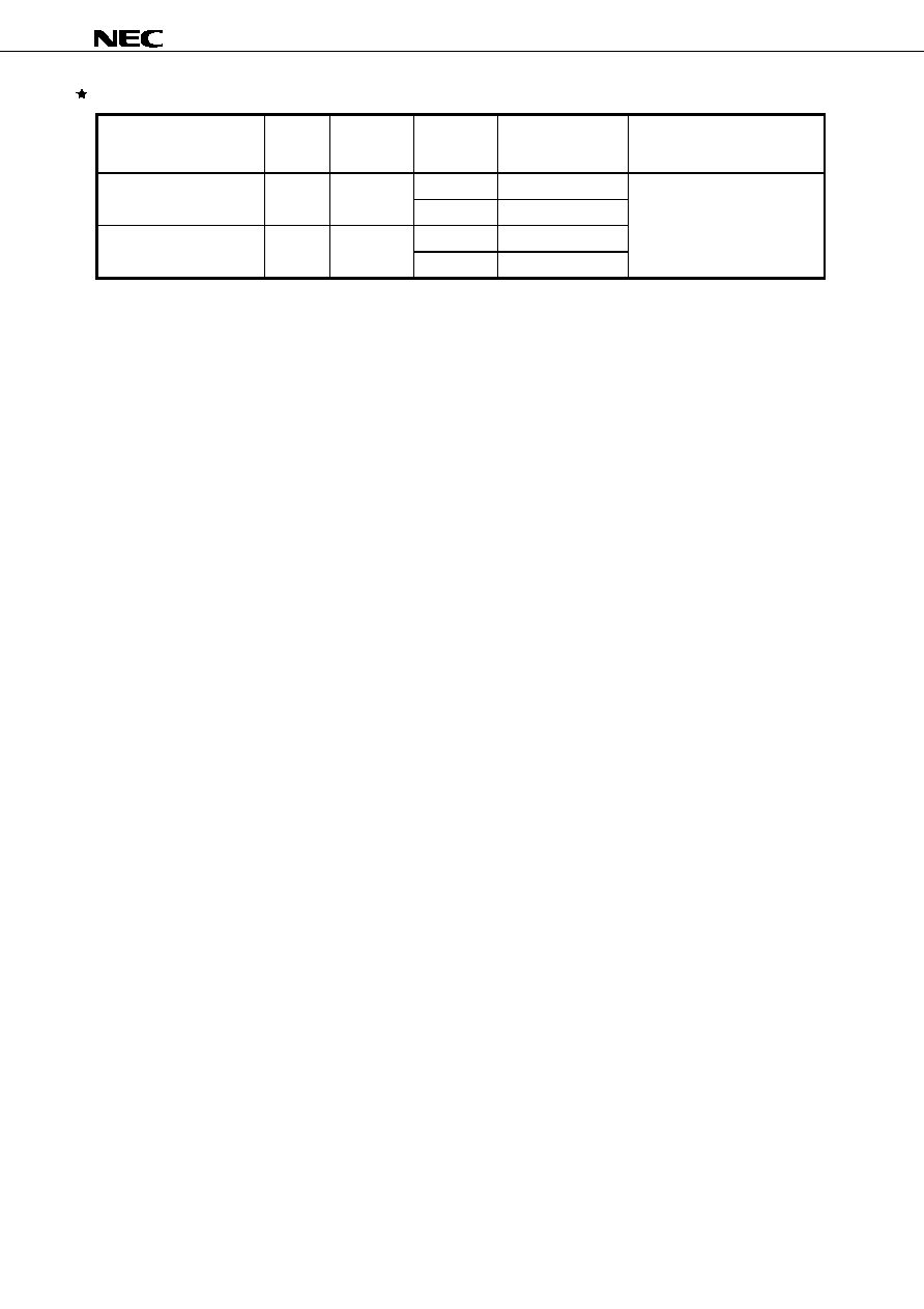
Pin Identifications
[
µ
PD44321182GF]
Symbol Pin
No.
Description
A0 to A20
37, 36, 35, 34, 33, 32, 100, 99, 82, 81, 44, Synchronous Address Input
45, 46, 47, 48, 49, 50, 83, 84, 43, 80
I/O1 to I/O16
58, 59, 62, 63, 68, 69, 72, 73, 8, 9, 12, 13, Synchronous Data In,
18, 19, 22, 23
Synchronous / Asynchronous Data Out
I/OP1, I/OP2
74, 24
Synchronous Data In (Parity),
Synchronous / Asynchronous Data Out (Parity)
ADV
85
Synchronous Address Load / Advance Input
/CE, CE2, /CE2
98, 97, 92
Synchronous Chip Enable Input
/WE
88
Synchronous Write Enable Input
/BW1, /BW2
93, 94
Synchronous Byte Write Enable Input
/G
86
Asynchronous Output Enable Input
CLK 89
Clock
Input
/CKE
87
Synchronous Clock Enable Input
MODE
31
Asynchronous Burst Sequence Select Input
Have to tied to V
DD
or V
SS
during normal operation
ZZ
64
Asynchronous Power Down State Input
V
DD
14, 15, 16, 41, 65, 66, 91
Power Supply
V
SS
17, 40, 67, 90
Ground
V
DD
Q
4, 11, 20, 27, 54, 61, 70, 77
Output Buffer Power Supply
V
SS
Q
5, 10, 21, 26, 55, 60, 71, 76
Output Buffer Ground
NC
1, 2, 3, 6, 7, 25, 28, 29, 30, 38, 39, 42, 51, No Connection
52, 53, 56, 57, 75, 78, 79, 95, 96