Document Outline
- COVER
- ˛ˇ
- ˛ˇ
- Pin Configuration
- Block Diagram
- ˛ˇ
- ˛ˇ
- ˛ˇ
- ˛ˇ
- ˛ˇ
- ˛ˇ
- ˛ˇ
- ˛ˇ
- 4.5 /WE Control
- ˛ˇ
- ˛ˇ
- ˛ˇ
- ˛ˇ
- ˛ˇ
- 4.10.1 Feature of /WAIT Output
- ˛ˇ
- ˛ˇ
- ˛ˇ
- ˛ˇ
- ˛ˇ
- ˛ˇ
- ˛ˇ
- ˛ˇ
- ˛ˇ
- ˛ˇ
- ˛ˇ
- ˛ˇ
- ˛ˇ
- ˛ˇ
- ˛ˇ
- ˛ˇ
- ˛ˇ
- ˛ˇ
- ˛ˇ
- ˛ˇ
- ˛ˇ
- ˛ˇ

The information in this document is subject to change without notice. Before using this document, please
confirm that this is the latest version.
Not all products and/or types are available in every country. Please check with an NEC Electronics
sales representative for availability and additional information.
Document No. M17507EJ2V0DS00 (2nd edition)
Date Published September 2005 CP (K)
Printed in Japan
MOS INTEGRATED CIRCUIT
PD46128512-X
128M-BIT CMOS MOBILE SPECIFIED RAM
8M-WORD BY 16-BIT
EXTENDED TEMPERATURE OPERATION
PRELIMINARY DATA SHEET
2005
The mark shows major revised points.
Description
The
PD46128512-X is a high speed, low power, 134,217,728 bits (8,388,608 words by 16 bits) CMOS Mobile
Specified RAM featuring asynchronous page read and random write, synchronous burst read/write function.
The
PD46128512-X is fabricated with advanced CMOS technology using one-transistor memory cell.
Features
∑ 8,388,608 words by 16 bits organization
∑ Asynchronous page read mode
∑ Synchronous read and write mode
∑ Burst length: 8 words / 16 words / continuous
∑ Clock latency: 5, 6, 7, 8, 9, 10
∑ Burst sequence: Linear burst
∑ Max clock frequency: 108/83 MHz
∑ Byte data control: /LB (DQ0 to DQ7), /UB (DQ8 to DQ15)
∑ Low voltage operation: 1.7 to 2.0 V
∑ Operating ambient temperature: T
A
=
-30 to +85 ∞C
∑ Chip Enable input: /CE1 pin
∑ Standby Mode input: CE2 pin
∑ Standby Mode 1: Normal standby (Memory cell data hold valid)
∑ Standby Mode 2: Density of memory cell data hold is variable
PD46128512 Clock Asynchronous
Operating
Operating
Supply current
frequency
initial
access
supply
ambient
At operating
At standby
A
MHz
time
voltage
temperature
mA
(MAX.) (TYP.)
(MAX.)
ns V ∞C
(MAX.)
Density of data hold
Density of data hold
(MAX.)
128M 32M 16M
8M 0M 128M 32M 16M
8M 0M
bits bits bits bits bits bits bits bits bits bits
-E9X
Note
108
70
1.7 to 2.0
-30 to +85
60
250 T.B.D. T.B.D. T.B.D. 65 80 T.B.D. T.B.D. T.B.D. 15
-E10X
Note
85 50
-E11X 83
70
60
-E12X
85
50
Note Under consideration

Preliminary Data Sheet M17507EJ2V0DS
2
PD46128512-X
Ordering Information
PD46128512-X is mainly shipping by wafer.
Please consult with our sales offices for package samples and ordering information.
Preliminary Data Sheet M17507EJ2V0DS
3
PD46128512-X
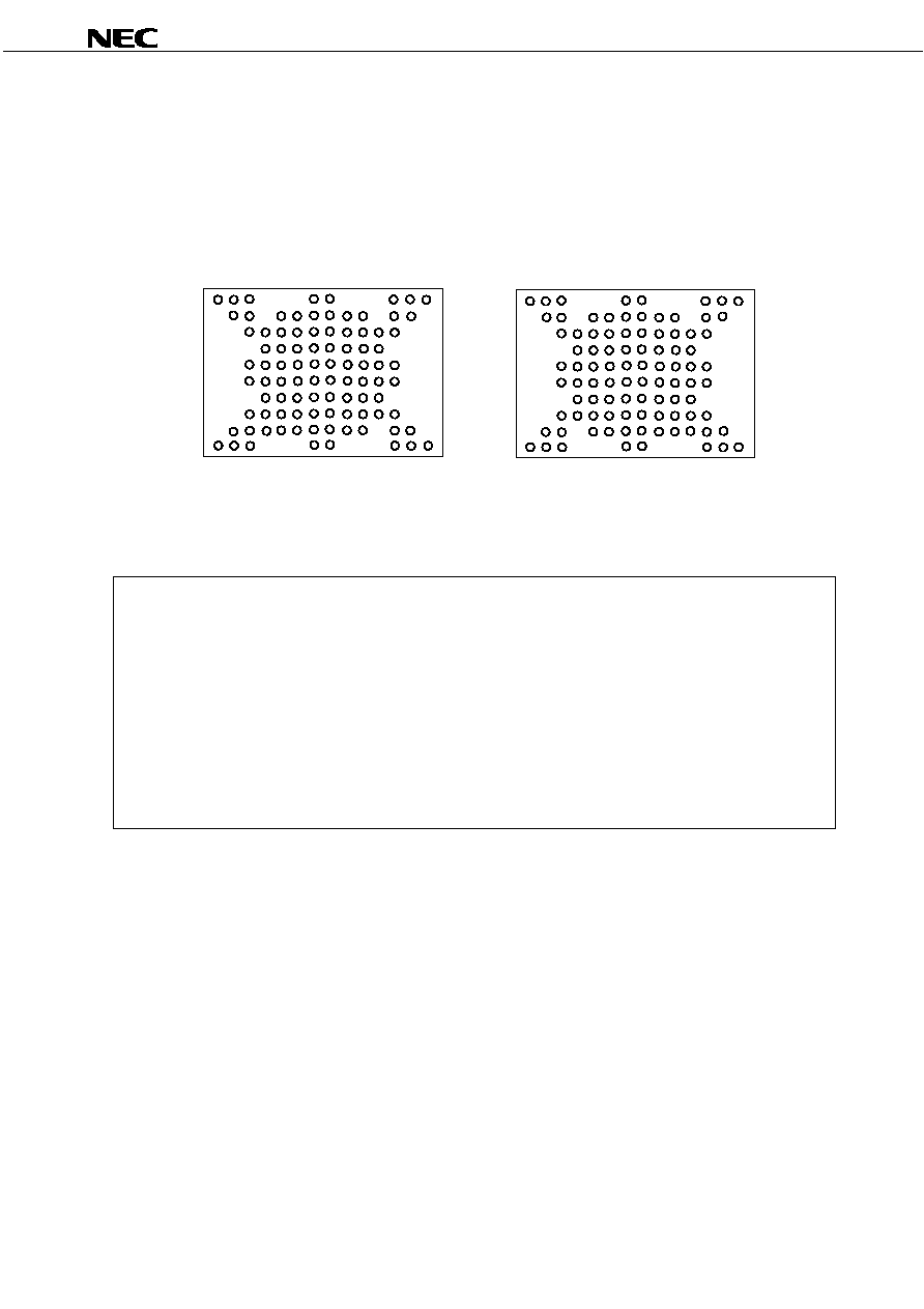
Pin Configuration
The following is pin configuration of package sample.
/xxx indicates active low signal.
93-PIN TAPE FBGA (12x9)
Top View
GND
DQ9
DQ5
A7
/OE
DQ7
DQ4
DQ0
A6
A18
A11
A8
A5
DQ8
DQ12
A13
A17
NC
NC
DQ10
V
CC
/WE
V
CC
A16
DQ11
/WAIT
/ADV
A12
DQ6
DQ13
A9
A15
A19
DQ14
/CE1
DQ15
DQ1
A1
A2
A4
A10
NC
DQ2
A0
A3
CE2
A20
A14
/LB
NC
CLK
/UB
DQ3
A21
A22
Vss
A
B
C
D
E
F
G
H
NC
NC
NC
NC
NC
NC
NC
NC
NC
NC
NC
NC
NC
M
K
L
J
10
9
8
7
6
5
4
3
2
1
NC
NC
NC
NC
NC
NC
NC
NC
NC
NC
NC
NC
L K J H G F E D C B A
M
B C D E F G H J K L M
10
9
8
7
6
5
4
3
2
1
A
Top View
Bottom View
N
P
N P
NC
NC
NC
NC
N
P
NC
NC
NC
NC
NC
NC
NC
NC
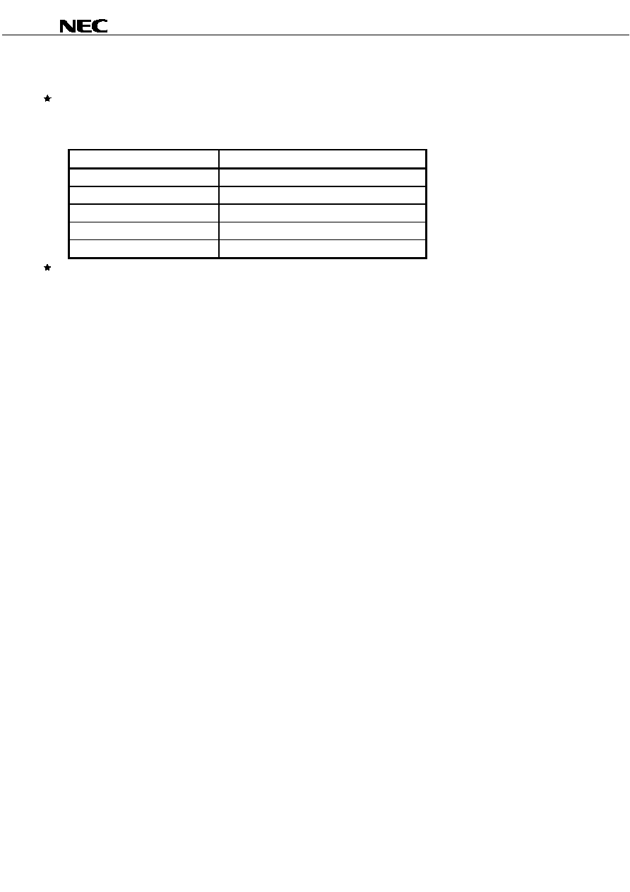
A0 to A22
: Address inputs
CLK
: Clock input
DQ0 to DQ15 : Data inputs / outputs
/ADV
: Address Valid Input
/CE1
: Chip select input
/WAIT
: Wait output
CE2
: Standby mode input
V
CC
: Power supply
/WE
: Write enable input
GND
: Ground
/OE
: Output enable input
NC
Note
: No Connection
/LB, /UB
: Byte data select input
Note Some signals can be applied because this pin is not internally connected.
Remark Refer to Package Drawing for the index mark.

Preliminary Data Sheet M17507EJ2V0DS
4
PD46128512-X
Block Diagram
A0
A22
DQ8 to DQ15
/WE
/OE
/UB
/LB
DQ0 to DQ7
V
CC
Q
GND
CE2
Standby mode control
Refresh
control
Refresh
counter
Address buffer
Address latch
Row
decoder
Input data
controller
Internal state
control
Output data
controller
Sense amplifier /
Switching circuit
Memory cell array
Column decoder
134,217,728 bits
/CE1
/ADV
CLK
/WAIT
V
CC
to

Preliminary Data Sheet M17507EJ2V0DS
5
PD46128512-X
Truth Table
Asynchronous Operation
Mode
/CE1 CE2 /ADV /OE /WE /LB /UB
DQ
/WAIT
DQ0
to
DQ7
DQ8
to
DQ15
Not selected (Standby Mode 1)
H
H
◊ ◊ ◊ ◊ ◊ High-Z High-Z
High-Z
Not selected (Standby Mode 2)
Note1
◊
L
◊ ◊ ◊ ◊ ◊ High-Z High-Z
High-Z
Word read
L
H
Note3
L H L L D
OUT
D
OUT
High-Z
Lower byte read
L
H
D
OUT
High-Z
High-Z
Upper byte read
H
L
High-Z
D
OUT
High-Z
Output
disable
H H High-Z High-Z High-Z
Output disable
H
◊
◊ High-Z High-Z
High-Z
Word write
L L L D
IN
D
IN
High-Z
Lower byte write
L
H
D
IN
High-Z
High-Z
Upper byte write
H
L
High-Z
D
IN
High-Z
Abort write
Note2
H H High-Z High-Z High-Z
Notes 1. CE2 pin must be fixed HIGH except Standby Mode 2 (refer to 2.3 Standby Mode Status Transition).
2. If /WE = LOW and /LB = /UB = HIGH, memory does not accept write data, so write operation is not available.
3.
Fixed LOW or toggle HIGH
LOW HIGH
Remark H, HIGH : V
IH
, L, LOW : V
IL
,
◊: V
IH
or V
IL
Clock pin must be fixed either LOW or HIGH.

Preliminary Data Sheet M17507EJ2V0DS
6
PD46128512-X
Burst Operation
Mode /CE1
CE2
CLK
/ADV
/OE
/WE
/LB
/UB
DQ
/WAIT
DQ0 to DQ7 DQ8 to DQ15
Note8
Not selected (Standby Mode 1)
H
H
◊ ◊ ◊ ◊ ◊ ◊ High-Z High-Z
High-Z
Not selected (Standby Mode 2)
Note1
◊ L
◊ ◊ ◊ ◊ ◊ ◊ High-Z High-Z
High-Z
Start address latch
L
H
Note4
L
◊
Note7
◊
Note7
◊
Note9
◊
Note9
High-Z
Note5
High-Z
Note5
◊
Advanced burst read to next address
H
L
H
D
OUT
D
OUT
Output
Note4
Valid
Burst read suspend
Note2
H High-Z High-Z HIGH
Burst read resume
Note2
L D
OUT
D
OUT
HIGH
Burst read termination
Note3
◊
◊ High-Z High-Z
High-Z
Advanced burst write to next address
L
H
L D
IN
D
IN
Output
Note4
Valid
Burst write suspend
Note2
H High-Z High-Z
HIGH
Burst write resume
Note2
L D
IN
D
IN
HIGH
Burst write termination
Note3
◊
◊ High-Z High-Z
High-Z
Abort write
Note6
L
◊
◊
Note10
HIGH
HIGH
High-Z High-Z
HIGH
Notes 1.
CE2 pin must be fixed HIGH except Standby Mode 2 (refer to 2.3 Standby Mode Status Transition).
2.
Be sure to suspend or resume a burst read after outputting the first read access data.
Be sure to suspend or resume a burst write after latching the first write data.
Burst write suspend or resume is available when setting WC = 1 (/WE level control) through Mode Register
Set.
3.
/CE1 must be fixed HIGH during t
TRB
specification until next read or write operation.
4.
Valid clock edge shall be set either positive or negative edge through Mode Register Set.
5.
If /OE = LOW and /LB = /UB = LOW, output is valid. If /OE = LOW and /LB = /UB = HIGH, output is high
impedance.
If /WE = LOW, output is high impedance. If /OE = /WE = HIGH, output is high impedance.
6. If /WE = LOW and /LB = /UB = HIGH, memory does not accept write data, so write operation is not
available.
7.
Both of two pins (/OE and /WE) or either of two should be connected to HIGH. It is prohibited to bring the
both /OE and /WE to LOW.
8.
Refer to the 4.10 /WAIT.
9. For the Burst Read, the /UB, /LB setup time to CLK (t
BC
) must be satisfied. For the Burst Write, the /UB,
/LB setup time to CLK (t
BC
) must be satisfied. Once /LB and /UB inputs are determined, they must not be
changed until the end of burst operation.
10. In case of WC = 0, /WE is HIGH.
In case of WC = 1, /WE is LOW.
The explanation of WC refers to Table 5-2. Mode Register Definition (5th Bus Cycle) and 5.9 /WE
control.
Remark H, HIGH : V
IH
, L, LOW : V
IL
,
◊: V
IH
or V
IL
,
: valid edge

Preliminary Data Sheet M17507EJ2V0DS
7
PD46128512-X
CONTENTS
1. Initialization .................................................................................................................................................. 9
2. Partial Refresh ........................................................................................................................................... 11
2.1 Standby Mode.......................................................................................................................................................... 11
2.2 Density Switching .................................................................................................................................................... 11
2.3 Standby Mode Status Transition.............................................................................................................................. 11
2.4 Addresses for Which Partial Refresh Is Supported.................................................................................................. 13
3. Page Read Operation ................................................................................................................................ 14
3.1 Features of Page Read Operation ........................................................................................................................... 14
3.2 Page Length ............................................................................................................................................................ 14
3.3 Page-Corresponding Addresses.............................................................................................................................. 14
3.4 Page Start Address.................................................................................................................................................. 14
3.5 Page Direction ......................................................................................................................................................... 14
3.6 Interrupt during Page Read Operation..................................................................................................................... 14
3.7 When Page Read is not Used.................................................................................................................................. 14
4. Burst Operation ......................................................................................................................................... 15
4.1 Features of Burst Operation .................................................................................................................................... 15
4.2 Burst Length ............................................................................................................................................................ 15
4.3 Latency .................................................................................................................................................................... 15
4.4 Single Write ............................................................................................................................................................. 17
4.5 /WE Control ............................................................................................................................................................. 17
4.6 Burst Read Suspend/Resume ................................................................................................................................. 18
4.7 Burst Write Suspend/Resume ................................................................................................................................. 19
4.8 Burst Read Termination........................................................................................................................................... 20
4.9 Burst Write Termination ........................................................................................................................................... 21
4.10 /WAIT..................................................................................................................................................................... 22
4.10.1
Feature of /WAIT Output ............................................................................................................................. 22
4.10.2
Dummy Wait Cycles at Continuous Burst Operation ................................................................................... 25
4.11 Reset Function from Synchronous Burst Mode to Asynchronous Page Mode....................................................... 27
5. Mode Register Settings............................................................................................................................. 28
5.1 Mode Register Setting Method ................................................................................................................................ 28
5.2 Cautions for Setting Mode Register ......................................................................................................................... 28
5.3 Partial Refresh Density ............................................................................................................................................ 30
5.4 Burst Length ............................................................................................................................................................ 30
5.5 Function Mode......................................................................................................................................................... 30
5.6 Valid Clock Edge ..................................................................................................................................................... 30
5.7 Read Latency (Write Latency) ................................................................................................................................. 30
5.8 Single Write ............................................................................................................................................................. 30
5.9 /WE Control ............................................................................................................................................................. 31
5.10 Reset to Page Mode .............................................................................................................................................. 31
5.11 Reserved Bits ........................................................................................................................................................ 31
5.12 Cautions for Timing Chart of Setting Mode Register.............................................................................................. 32
6. Electrical Specifications ........................................................................................................................... 33

Preliminary Data Sheet M17507EJ2V0DS
8
PD46128512-X
7. Asynchronous AC Specification, Timing Chart ..................................................................................... 36
8. Synchronous AC Specification, Timing Chart........................................................................................ 57
9. Mode Register Setting Timing.................................................................................................................. 74
10. Standby Mode Timing Chart................................................................................................................... 77
11. Package Drawing..................................................................................................................................... 78
12. Recommended Soldering Conditions ................................................................................................... 79

Preliminary Data Sheet M17507EJ2V0DS
9
PD46128512-X
1. Initialization
Initialize the
PD46128512-X at power application using the following sequence to stabilize internal circuits.
There are 2 method of initialization.
Initialization Timing 1
(1) Following power application, make CE2 HIGH after fixing CE2 to LOW for the period of t
VHMH
.
Make /CE1 HIGH before making CE2 HIGH.
(2) /CE1 and CE2 are fixed HIGH for the period of t
MHCL
.
Normal operation is possible after the completion of initialization.
Figure 1-1. Initialization Timing Chart 1
/CE1 (Input)
CE2 (Input)
t
MHCL
Intialization
t
CHMH
t
VHMH
Nomal Operation
V
CC
, V
CC
Q
V
CC
(MIN.), V
CC
Q (MIN.)
Cautions 1. Make CE2 LOW when starting the power supply.
2.
t
VHMH
is specified from when the power supply voltage reaches the prescribed minimum value
(V
CC
(MIN.), V
CC
Q (MIN.)).
Initialization Timing 1
Parameter Symbol
MIN.
MAX.
Unit
Power application to CE2 LOW hold
t
VHMH
50
s
/CE1 HIGH to CE2 HIGH
t
CHMH
0
ns
Following power application CE2 HIGH hold to /CE1 LOW
t
MHCL
300
s

Preliminary Data Sheet M17507EJ2V0DS
10
PD46128512-X
Initialization Timing 2
(1) Following power application, make CE2 and /CE1 HIGH for the period of t
MHCL
.
Normal operation is possible after the completion of initialization.
Figure 1-2. Initialization Timing Chart 2
t
MHCL
/CE1 (Input)
CE2 (Input)
Intialization
Nomal Operation
V
CC
, V
CC
Q
V
CC
(MIN.), V
CC
Q (MIN.)
Cautions 1. t
MHCL
is specified from when the power supply voltage reaches the prescribed minimum value
(V
CC
(MIN.), V
CC
Q (MIN.)).
2. If the period from power supplying to value V
CC
(MIN.), V
CC
Q (MIN.) is beyond 10 ms or power
supply is not stable rise, should be used Initialization Timing Chart 1.
Initialization Timing 2
Parameter Symbol
MIN.
MAX.
Unit
Following power application /CE1, CE2 HIGH hold to /CE1 LOW
t
MHCL
300
s

Preliminary Data Sheet M17507EJ2V0DS
11
PD46128512-X
2. Partial Refresh
2.1 Standby Mode
In addition to the regular standby mode (Standby Mode 1) with a 128M bits density, Standby Mode 2, which performs
partial refresh, is also provided.
2.2 Density Switching
In Standby Mode 2, the densities that can be selected for performing refresh are 32M bits, 16M bits, 8M bits, and 0M
bit.
The density for performing refresh can be set with the mode register. Once the refresh density has been set in the
mode register, these settings are retained until they are set again, while applying the power supply. However, the mode
register setting will become undefined if the power is turned off, so set the mode register again after power application.
(For how to perform mode register settings, refer to section 5. Mode Register Settings.)
2.3 Standby Mode Status Transition
In Standby Mode 1, /CE1 and CE2 are HIGH. In Standby Mode 2, CE2 is LOW. In Standby Mode 2, if 0M bit is set as
the density, it is necessary to perform initialization the same way as after applying power, in order to return to normal
operation from Standby Mode 2. When the density has been set to 32M bits, 16M bits, or 8M bits in Standby Mode 2, it is
not necessary to perform initialization to return to normal operation from Standby Mode 2.
For the timing charts, refer to Figure 10-1. Standby Mode 2 Entry / Exit Timing Chart (Asynchronous Mode),
Figure 10-2. Standby Mode 2 (data not held) Entry / Exit Timing Chart (Asynchronous Mode).

Preliminary
Data Sheet M17507EJ2V0DS
12
PD46128512-X
Note Case "Initialization Timing 2" : Following initialization, set mode register.
Figure 2-1. Standby Mode State Machine
Power On
Active
/CE1 = V
IH
,
CE2 = V
IH
Standby
Mode1
/CE1 = V
IH
,
CE2 = V
IL
Burst Mode
Burst Mode
CE2 = V
IL
CE2 = V
IL
(RP=1)
/CE1 = V
IL
,
CE2 = V
IH
/CE1 = V
IH
,
CE2 = V
IH
/CE1 = V
IH
,
CE2 = V
IL
/CE1 = V
IH
,
CE2 = V
IH
/CE1 = V
IL
,
CE2 = V
IH
/CE1 = V
IH
,
CE2 = V
IH
/CE1 = V
IH
,
CE2 = V
IH
/CE1 = V
IH
,
CE2 = V
IL
(RP=1)
/CE1 = V
IH
,
CE2 = V
IL
(RP=1)
/CE1 = V
IH
,
CE2 = V
IH
/CE1 = V
IH
,
CE2 = V
IL
(RP=0)
CE2 = V
IL
(RP=0)
Mode Register
Setting
CE2 = V
IL
(RP=0)
/CE1 = V
IH
,
CE2 = V
IL
(RP=0)
Initialize
Note
Standby Mode2
(Data not held)
Active
Standby
Mode1
Standby Mode2
(32Mbit/16Mbit/8Mbit)
Standby Mode2
(32Mbit/16Mbit/8Mbit)
Standby Mode2
(Data not held)
Page Mode
Initialize
CE2 = V
IL
CE2 = V
IL
(RP=1)
Page Mode

Preliminary Data Sheet M17507EJ2V0DS
13
PD46128512-X
2.4 Addresses for Which Partial Refresh Is Supported
Data hold density
Correspondence address
32M bits
000000H to 1FFFFFH
16M bits
000000H to 0FFFFFH
8M bits
000000H to 07FFFFH
Preliminary Data Sheet M17507EJ2V0DS
14
PD46128512-X
3. Page Read Operation
For the timing charts, refer to Figure 7-10. Asynchronous Page Read Cycle Timing Chart.
3.1 Features of Page Read Operation
Features Item
Page length
16 words
Page read-corresponding addresses
A3, A2, A1, A0
Page read start address
Don't care
Page direction
Don't care
Interrupt during page read operation
Enabled
Note
Note /CE1 = HIGH, or any change in address A4 or higher will initiate a new read access specified as t
AA
or t
ACE
.
3.2 Page Length
16 words is supported as the page lengths. Page length is not necessary to set through Mode Register.
3.3 Page-Corresponding Addresses
The 16 words page read-enabled addresses are A3, A2, A1, and A0. Fix addresses other than A3, A2, A1, and A0
during page read operation.
3.4 Page Start Address
Since random page read is supported, any address (A3, A2, A1 and A0 with the 16 words page) can be used as the
page read start address.
3.5 Page Direction
Since random page read is possible, there is not restriction on the page direction.
3.6 Interrupt during Page Read Operation
When generating an interrupt during page read, make /CE1 HIGH or change A4 and higher addresses.
3.7 When Page Read is not Used
Since random page read is supported, even when not using page read, random access is possible as usual.

Preliminary Data Sheet M17507EJ2V0DS
15
PD46128512-X
4. Burst Operation
Burst operation is valid when burst mode is set through mode register.
4.1 Features of Burst Operation
Function Features
Burst Length
8, 16, Continuous
Read Latency
5, 6, 7, 8, 9, 10
Write Latency
4, 5, 6, 7, 8, 9
Burst Sequence
Linear
Single Write
Single Write, Burst Write
Valid Clock Edge
Rising Edge, Falling Edge
4.2 Burst Length
Burst length is the number of word to be read or written during synchronous burst read/write operation as the result of a
single address latch cycle. It can be set on 8, 16words boundary or continuous for entire address through Mode Register
Set sequence. Starting from initial address being latched, device internal address counter assign +1 to the previous
address until reaching the end of boundary address. After completing read data out or write data latch for the set burst
length, operation automatically end except for continuous burst. When continuous burst length is set, read /write is
endless unless it is terminated by the rising edge of /CE1.
4.3 Latency
Read Latency (RL) is the number of clock cycles between the address being latched and first read data becoming
available during synchronous burst read operation. It is set through Mode Register Set sequence after power application.
Once RL is set through Mode Register Set sequence, write latency, that is the number of clock cycles between address
being latched and first write data being latched, is automatically set to RL
-1.
Latency Count
Grade
Clock
Asynchronous
Read Latency
Write Latency
Note
Frequency
access
time
-E9X
<108 MHz
70 ns
8, 9, 10
7, 8, 9
-E10X
85
ns 10
9
-E9X, -E11X
<83 MHz
70 ns
7, 8, 9, 10
6, 7, 8, 9
-E10X, -E12X
85 ns
8, 9, 10
7, 8, 9
-E9X, -E11X
<66 MHz
70 ns
6, 7, 8, 9, 10
5, 6, 7, 8, 9
-E10X, -E12X
85 ns
7, 8, 9, 10
6, 7, 8, 9
-E9X, -E11X
<52 MHz
70 ns
5, 6, 7, 8, 9, 10
4, 5, 6, 7, 8, 9
-E10X, -E12X
85 ns
5, 6, 7, 8, 9, 10
4, 5, 6, 7, 8, 9
Note Write Latency = Read Latency
-1

Preliminary Data Sheet M17507EJ2V0DS
16
PD46128512-X
Figure 4-1. Latency Definition
Valid
CLK (Input)
/ADV (Input)
Address (Input)
/CE1 (Input)
DQ (Output)
DQ (Input)
RL = 5
DQ (Output)
DQ (Input)
RL = 6
DQ (Output)
DQ (Input)
RL = 7
DQ (Output)
DQ (Input)
RL = 8
DQ (Output)
DQ (Input)
RL = 9
DQ (Output)
DQ (Input)
RL = 10
Q1
Q3
High-Z
Q0
Q2
Q4
Q5
D1
D3
D0
D2
D4
D5
D6
High-Z
Write Latency = 4
Read Latency = 5
High-Z
High-Z
Write Latency = 5
Read Latency = 6
Q1
Q3
High-Z
Q0
Q2
Q4
D1
D3
D0
D2
D4
D5
High-Z
Write Latency = 6
Read Latency = 7
Q1
Q3
High-Z
Q0
Q2
D1
D3
D0
D2
D4
High-Z
Write Latency = 7
Read Latency = 8
Q1
High-Z
Q0
Q2
D1
D3
D0
D2
High-Z
Write Latency = 8
Read Latency = 9
Q1
High-Z
Q0
D1
D0
D2
Q0
D1
D0
High-Z
Write Latency = 9
Read Latency = 10

Preliminary Data Sheet M17507EJ2V0DS
17
PD46128512-X
4.4 Single Write
Single write operation is a single-word length synchronous write operation. The
PD46128512-X is supporting two
type of synchronous write operation, "Burst Read & Single Write" and "Burst Read & Burst Write", configurable with SW
bit in the mode register. When the device set to the "Burst Read & Single Write" operation mode, the burst length at the
synchronous write operation is always fixed to single word length regardless of the burst length (BL) setting in the mode
register, however, BL setting is still effective in synchronous read operation (Refer to 5. Mode Register Settings).
Refer to Figure 8-8. Synchronous Burst Write Cycle Timing Chart (/WE level Control), Figure 8-9.
Synchronous Burst Write Cycle Timing Chart (/WE single clock control), Figure 8-10. Synchronous Single Write
Timing Chart.
4.5 /WE Control
The
PD46128512-X is supporting two type of timing control with /WE input signal, "/WE level control" and "/WE single
clock control" configurable with WC bit in the mode register at synchronous write operation. In case of /WE level
controlling, /WE must be asserted LOW before the 2nd clock input timing (T1).
Refer to Figure 8-8. Synchronous Burst Write Cycle Timing Chart (/WE level Control), Figure 8-9.
Synchronous Burst Write Cycle Timing Chart (/WE single clock control).
Figure 4-2. /WE Control
T1
T3
T0
T2
T4
T5
T6
T7
CLK (Input)
/ADV (Input)
Address (Input)
/CE1 (Input)
/WE (Input)
DQ0 to DQ15 (Input)
/WAIT (Output)
/WE (Input)
DQ0 to DQ15 (Input)
/WAIT (Output)
/WE Level Control
/WE Single Clock Control
Add
Read Latency = 5
t
WES
High-Z
D0
D1
D2
D3
High-Z
t
WES
t
WEH
High-Z
D0
D1
D2
D3
High-Z
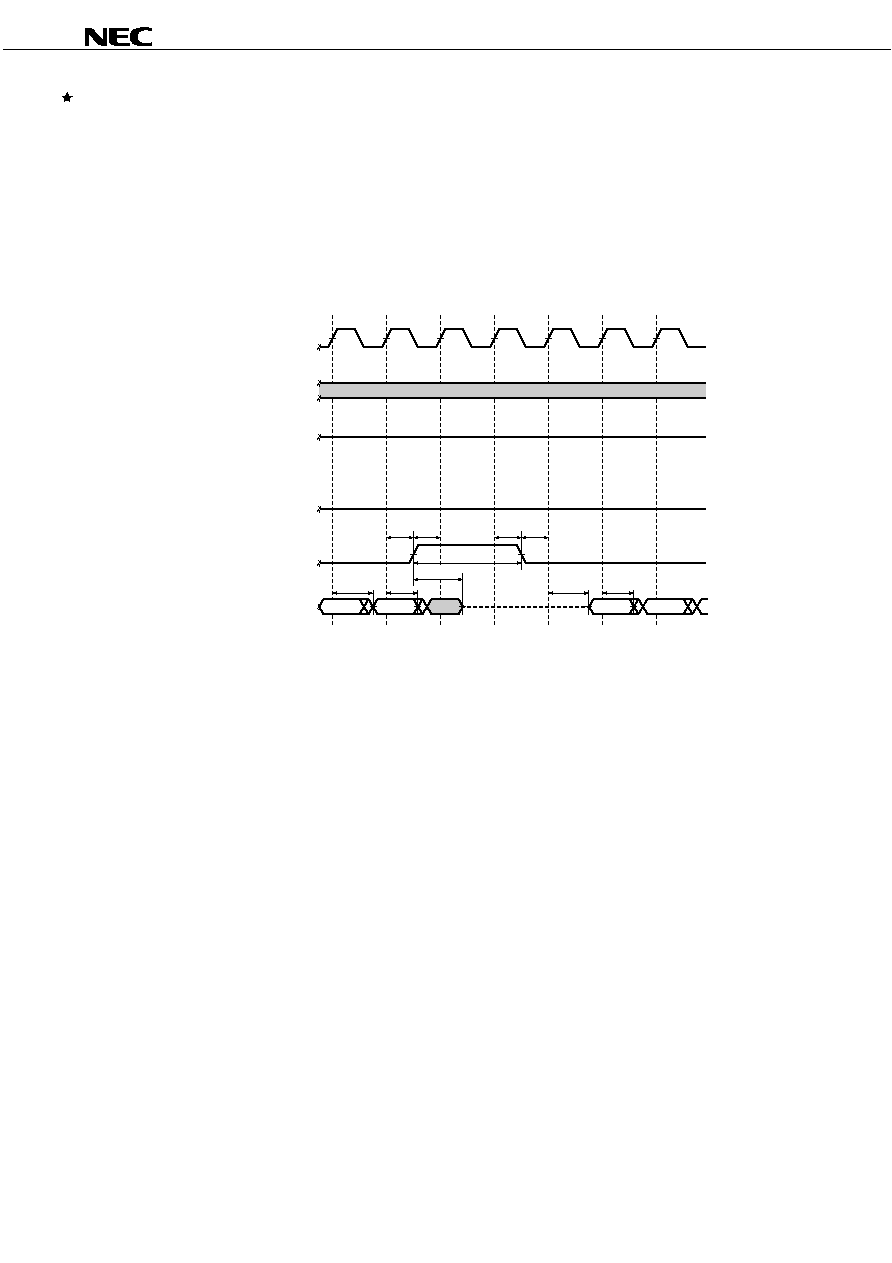
Preliminary Data Sheet M17507EJ2V0DS
18
PD46128512-X
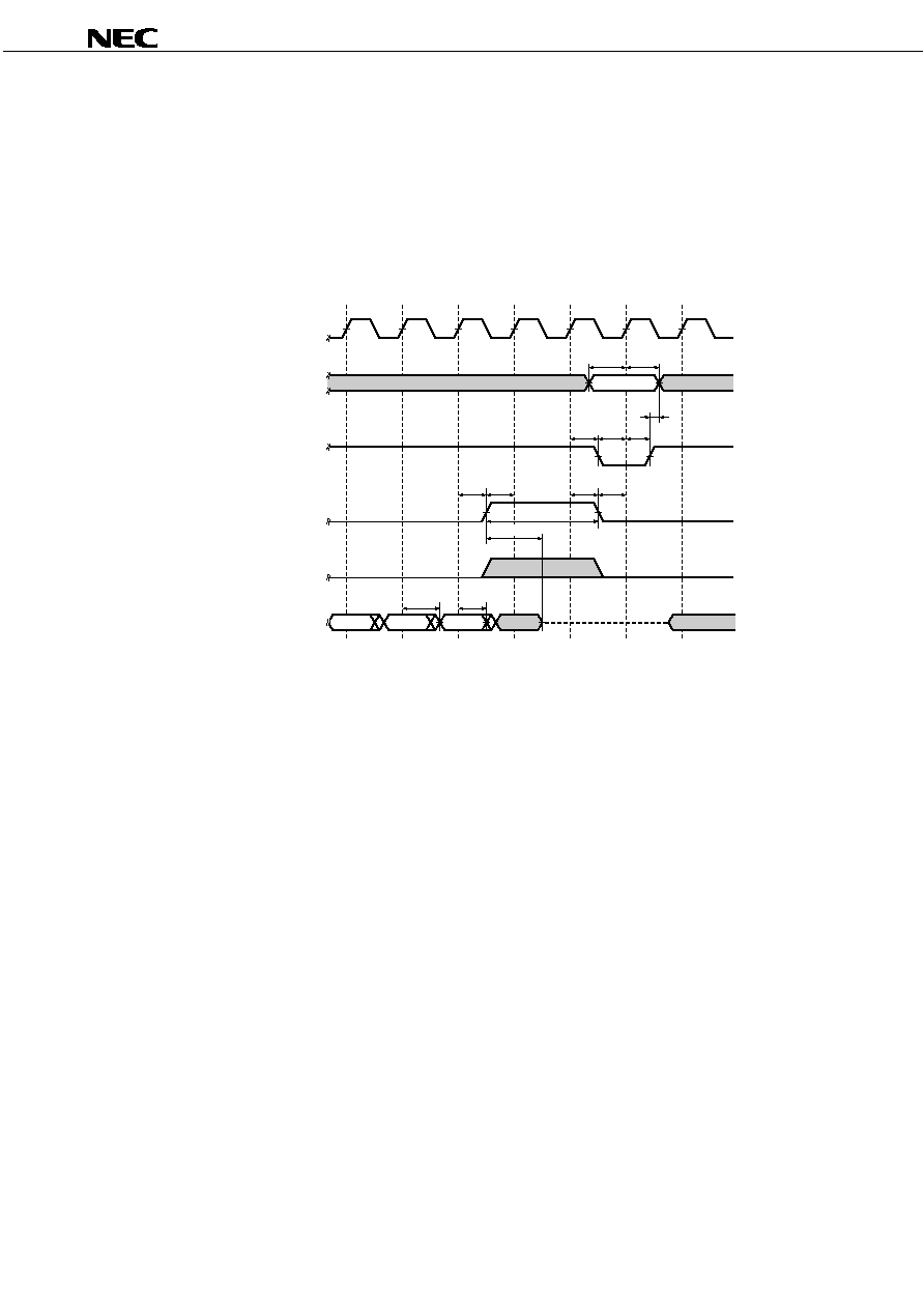
4.6 Burst Read Suspend/Resume
A burst read operation can be suspended by bringing /OE signal from LOW to HIGH during the burst read operation.
The /OE signal must be required to meet the specified setup / hold time to the clock which the data being suspended.
Once the /OE is brought to HIGH, output data turns to be high impedance state after specific time duration.
The burst read suspend will be effective after outputting first read data, or after outputting dummy wait cycles in case of
dummy wait cycling insertion at continuous burst read mode.
The burst suspend mode will be resumed by re-asserting /OE to LOW, and the first output data is from the same
address location as of being suspended.
Figure 4-3. Burst Read Suspend/Resume
CLK (Input)
/ADV (Input)
/OE (Input)
A0 to A22 (Input)
/CE1 (Input)
DQ0 to DQ15 (Output)
H
t
SOEH
t
SOES
t
SOP
t
SOEH
t
SOES
t
OHZ
L
High-Z
Q0
Q1
Q2
Q3
t
BDH
t
BACC
t
BDH
t
BACC

Preliminary Data Sheet M17507EJ2V0DS
19
PD46128512-X
4.7 Burst Write Suspend/Resume
A burst write operation can be suspended by bringing /WE signal from LOW to HIGH during the burst write operation.
The /WE signal must be required to meet the specified setup / hold time to the clock which the data being suspended.
The burst write suspend will be effective after inputting first write data.
The burst suspend mode will be resumed by re-asserting /WE to LOW, and the first write data is written to the same
address location as of being suspended. Burst write suspend or resume is available only when WC = 1(/WE level
control) is set to the mode register (refer to Table 5-2. Mode Register Definition (5th Bus Cycle).
Figure 4-4. Burst Write Suspend/Resume
T9
T8
T10
T4
T5
T6
T7
CLK (Input)
/ADV (Input)
/WE (Input)
A0 to A22 (Input)
/CE1 (Input)
DQ0 to DQ15 (Output)
H
t
WEH
t
WES
t
SWHP
t
WEH
t
WES
L
High-Z
D0
D1
D2
D3
t
WDH
t
WDS
t
WDH
t
WDS
Preliminary Data Sheet M17507EJ2V0DS
20
PD46128512-X
4.8 Burst Read Termination
Burst read termination can be performed by transferring /CE1 LOW to HIGH during the burst read. When continuous
burst length is set, burst read is endless unless it is terminated. Be sure to terminate a burst read after outputting the first
read access data.
In order to guarantee the last data output, the specified minimum value of /CE1 = LOW hold time (t
CEH
) against clock
edge must be satisfied. In order to perform next operation after burst read termination, the specified minimum value of
Burst Read Termination recovery time (t
TRB
) must be satisfied.
Figure 4-5. Burst Read Termination
CLK (Input)
/ADV (Input)
/OE (Input)
A0 to A22 (Input)
/CE1 (Input)
DQ0 to DQ15 (Output)
Valid
t
ACS
t
ACH
t
CHV
t
CSV
t
CHV
t
AH
t
CEH
t
CES
t
TRB
t
CEH
t
CES
t
CHZ
High-Z
Q2
Q1
Q3
t
BDH
t
BACC

Preliminary Data Sheet M17507EJ2V0DS
21
PD46128512-X
4.9 Burst Write Termination
Burst write termination can be performed by transferring /CE1 LOW to HIGH during the burst write. When continuous
burst length is set, burst write is endless unless it is terminated. Be sure to terminate a burst write after latching the first
write data.
In order to guarantee the last write data is latched, the specified minimum value of /CE1 = LOW hold time against clock
edge must be satisfied. In order to perform next operation after burst write termination, the specified minimum value of
Burst Write Termination recovery time (t
TRB
) must be satisfied.
Figure 4-6. Burst Write Termination
CLK (Input)
/ADV (Input)
/WE (Input)
A0 to A22 (Input)
/CE1 (Input)
DQ0 to DQ15 (Output)
Valid
t
ACS
t
ACH
t
CHV
t
CSV
t
CHV
t
AH
t
WRB
t
CEH
t
CES
t
TRB
t
CEH
t
CES
High-Z
D2
D1
D3
t
WDH
t
WDS

Preliminary Data Sheet M17507EJ2V0DS
22
PD46128512-X
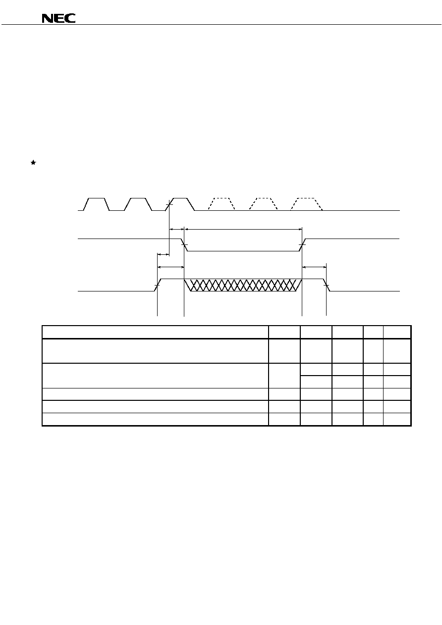
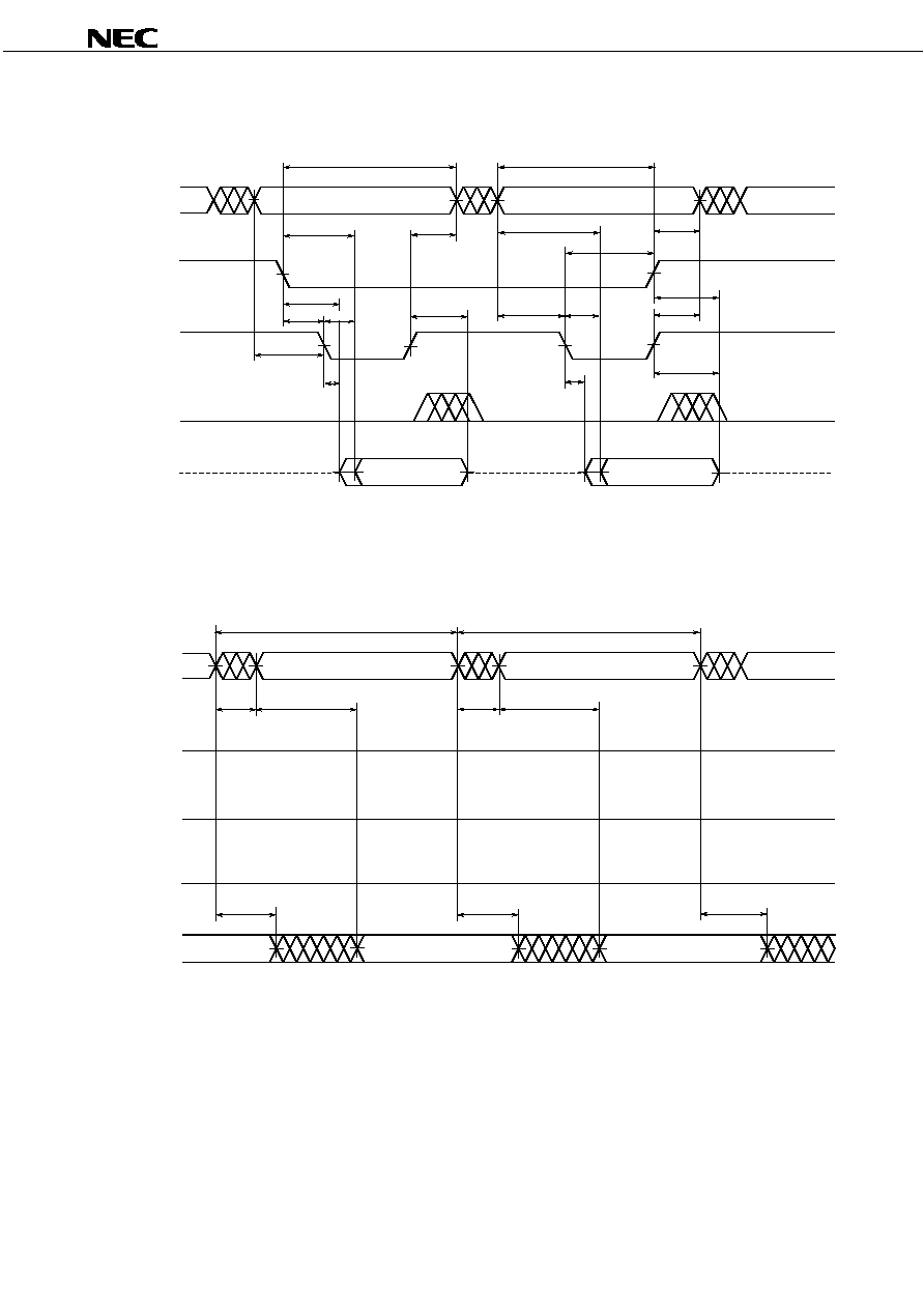
4.10 /WAIT
4.10.1
Feature of /WAIT Output
The /WAIT output signal indicates the internal status, busy (LOW) or ready (HIGH), during the burst read and burst
write operation.
The /WAIT output state changes depend on the /CE1 and /ADV condition. When /CE1 held entire LOW, the /WAIT
output corresponds with /ADV state and turns to LOW by /ADV assertion. The /WAIT output stays high impedance at
standby mode (/CE1 = HIGH) and turns to LOW at active mode brought by /CE1 assertion.
The /WAIT output will be asserted to LOW after specific time duration triggered by falling edge of /CE1, or falling edge
of /ADV when /CE1 held entire LOW. When the /WAIT output LOW, it indicates the output data is not valid at the next
clock cycle.
The /WAIT output asserts HIGH one clock cycle before the valid data output.
The /WAIT output retains the same state as of the clock cycle right before being suspended with /OE brought to HIGH.
Figure 4-7. Burst Read /WAIT Output (/CE1 = HIGH
LOW)
T1
T3
T0
T2
T4
T5
CLK (Input)
/ADV (Input)
A0 to A22 (Input)
/CE1 (Input)
/WE (Input)
DQ0 to DQ15 (Output)
/WAIT (Output)
Add
H
RL = 5
High-Z
Q0
High-Z
t
CEWA
t
CLWA

Preliminary Data Sheet M17507EJ2V0DS
23
PD46128512-X
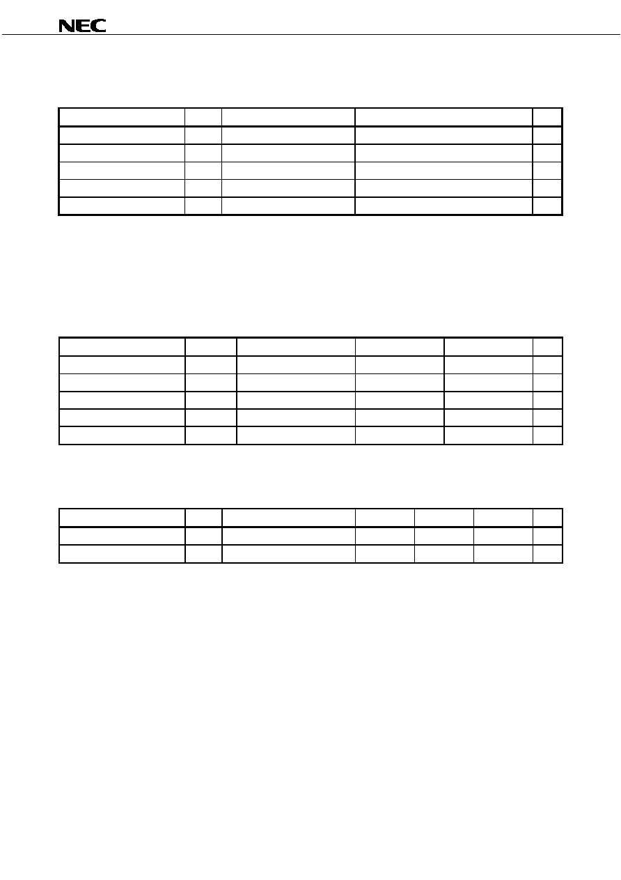
Figure 4-8. Burst Read /WAIT Output (/CE1 = LOW, /ADV = HIGH
LOW)
T1
T3
T0
T2
T4
T5
CLK (Input)
/ADV (Input)
A0 to A22 (Input)
/CE1 (Input)
/WE (Input)
DQ0 to DQ15 (Output)
/WAIT (Output)
Add
t
ADWA
L
H
RL = 5
High-Z
Q0
t
CLWA
The /WAIT output will be asserted to LOW after specific time duration from the falling edge of the /CE1, or falling edge
of the /ADV when /CE1 held LOW at burst write operation. When the /WAIT output LOW, it indicates the input data can
not be accepted at the next clock cycle. The /WAIT output asserts HIGH one clock cycle before the valid data input. The
/WAIT output retains the same state as of the clock cycle right before being suspended with /WE brought to HIGH.
The /WAIT output always stay high impedance state under asynchronous mode setting.

Preliminary Data Sheet M17507EJ2V0DS
24
PD46128512-X
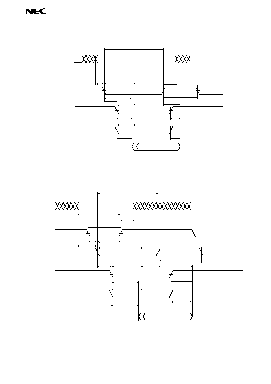
Figure 4-9. Burst Write /WAIT Output (/CE1 = HIGH
LOW)
T1
T3
T0
T2
T4
T5
CLK (Input)
/ADV (Input)
A0 to A22 (Input)
/CE1 (Input)
/WE (Input)
(WC = 1)
(WC = 0)
/WE (Input)
DQ0 to DQ15 (Output)
/WAIT (Output)
Add
t
WES
t
WES
t
WEH
RL = 5
High-Z
D0
D1
t
CLWA
High-Z
t
CEWA
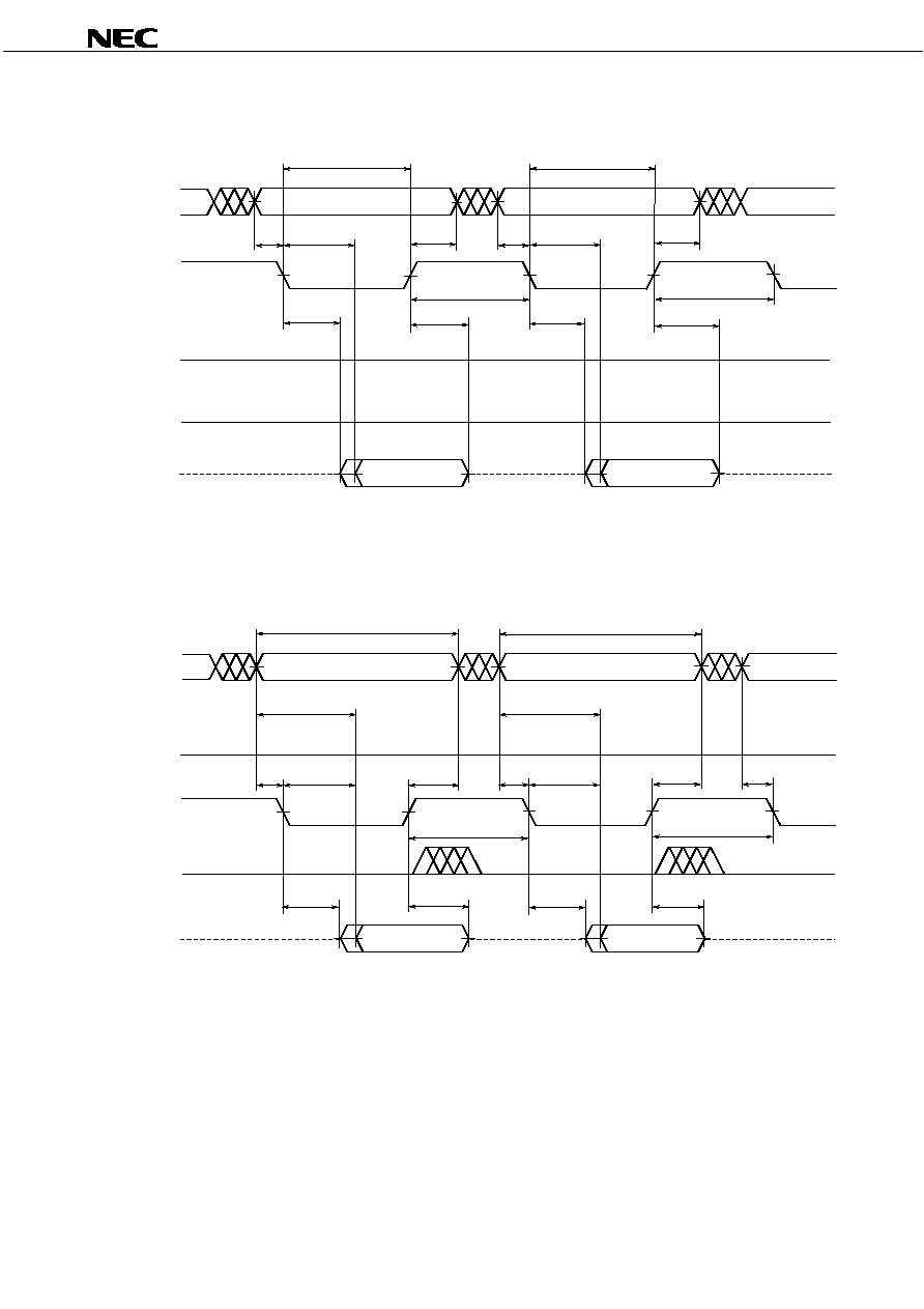
Figure 4-10. Burst Write /WAIT Output (/CE1 = LOW, /ADV = HIGH
LOW)
T1
T3
T0
T2
T4
T5
CLK (Input)
/ADV (Input)
A0 to A22 (Input)
/CE1 (Input)
/WE (Input)
(WC = 1)
(WC = 0)
/WE (Input)
DQ0 to DQ15 (Output)
/WAIT (Output)
Add
t
ADWA
t
WES
t
WES
t
WEH
RL = 5
High-Z
D0
D1
t
CLWA

Preliminary Data Sheet M17507EJ2V0DS
25
PD46128512-X
4.10.2
Dummy Wait Cycles at Continuous Burst Operation
In continuous burst operation, dummy wait cycles may be needed when a burst sequence crosses the first 16-word
boundary. Whether dummy wait cycles is needed or not depends on start address and the number of dummy wait cycles
depends on Read Latency (See Table 4-1. Burst Sequence and 4-2. Dummy Wait Cycles and Read Latency).
During the dummy cycle period, /WAIT output LOW.
Table 4-1. Burst Sequence
Start
Burst length = 8
Burst length = 16
Continuous
Address
Linear
Linear
Linear
xx00 H
0-1-2-3-4-5-6-7
0-1-2-3-4-5-6-7-8-9-10-11-12-13-14-15 0-1-2-3-4-5-6-7-8-9-10-11-12-13-14-15-...
xx01 H
1-2-3-4-5-6-7-0
1-2-3-4-5-6-7-8-9-10-11-12-13-14-15-0 1-2-3-4-5-6-7-8-9-10-11-12-13-14-15-16-...
xx02 H
2-3-4-5-6-7-0-1
2-3-4-5-6-7-8-9-10-11-12-13-14-15-0-1 2-3-4-5-6-7-8-9-10-11-12-13-14-15-16-17-...
xx03 H
3-4-5-6-7-0-1-2
3-4-5-6-7-8-9-10-11-12-13-14-15-0-1-2 3-4-5-6-7-8-9-10-11-12-13-14-15-16-17-18-...
xx04 H
4-5-6-7-0-1-2-3
4-5-6-7-8-9-10-11-12-13-14-15-0-1-2-3 4-5-6-7-8-9-10-11-12-13-14-15-16-17-18-19-...
xx05 H
5-6-7-0-1-2-3-4
5-6-7-8-9-10-11-12-13-14-15-0-1-2-3-4 5-6-7-8-9-10-11-12-13-14-15-16-17-18-19-20-...
xx06 H
6-7-0-1-2-3-4-5
6-7-8-9-10-11-12-13-14-15-0-1-2-3-4-5 6-7-8-9-10-11-12-13-14-15-16-17-18-19-20-21-...
xx07 H
7-0-1-2-3-4-5-6
7-8-9-10-11-12-13-14-15-0-1-2-3-4-5-6 7-8-9-10-11-12-13-14-15-16-17-18-19-20-21-22-...
xx08 H
8-9-10-11-12-13-14-15-0-1-2-3-4-5-6-7 8-9-10-11-12-13-14-15-16-17-18-19-20-21-22-23-...
xx09 H
9-10-11-12-13-14-15-0-1-2-3-4-5-6-7-8 9-10-11-12-13-14-15-16-17-18-19-20-21-22-23-24-...
xx0A H
10-11-12-13-14-15-0-1-2-3-4-5-6-7-8-9 10-11-12-13-14-15-16-17-18-19-20-21-22-23-24-25-...
xx0B H
11-12-13-14-15-0-1-2-3-4-5-6-7-8-9-10 11-12-13-14-15-W-16-17-18-19-20-21-22-23-24-25-...
xx0C H
12-13-14-15-0-1-2-3-4-5-6-7-8-9-10-11 12-13-14-15-W-W-16-17-18-19-20-21-22-23-24-25-...
xx0D H
13-14-15-0-1-2-3-4-5-6-7-8-9-10-11-12 13-14-15-W-W-W-16-17-18-19-20-21-22-23-24-25-...
xx0E H
14-15-0-1-2-3-4-5-6-7-8-9-10-11-12-13 14-15-W-W-W-W-16-17-18-19-20-21-22-23-24-25-...
xx0F H
15-0-1-2-3-4-5-6-7-8-9-10-11-12-13-14 15-W-W-W-W-W-16-17-18-19-20-21-22-23-24-25-...
xx10 H
... 16-17-18-19-20-21-22-23-24-25-26-...
xx11 H
17-18-19-20-21-22-23-24-25-26-27-...
...
...
...
...
xxnB H
-xxnB
-xxnC-xxnD-xxnE-xxnF-W-xx(n+1)0-xx(n+1)1-...
xxnC H
-xxnC-xxnD-xxnE-xxnF-W-W-xx(n+1)0-xx(n+1)1-...
xxnD H
-xxnD-xxnE-xxnF-W-W-W-xx(n+1)0-xx(n+1)1-...
xxnE H
-xxnE-xxnF-W-W-W-W-xx(n+1)0-xx(n+1)1-xx(n+1)2-...
xxnF H
-xxnF-W-W-W- W-W-xx(n+1)0-xx(n+1)1-xx(n+1)2-...
...
...
...
...
Remarks 1. The above table assumes Read Latency is set 5. W shows Dummy Wait Cycles.
2. Address is in HEX.

Preliminary Data Sheet M17507EJ2V0DS
26
PD46128512-X
Table 4-2. Dummy Wait Cycles and Read Latency
Start
Read Latency
Read Latency
Read Latency
Read Latency
Read Latency
Address
= 5
= 6
...
= 9
= 10
= n
(Write Latency
(Write Latency
(Write Latency
(Write Latency (Write
Latency
= 4)
= 5)
= 6)
= 7)
= n
-1)
xxx0 H
No wait
No wait
...
No wait
No wait
No wait
xxx1 H
No wait
No wait
...
No wait
No wait
No wait
xxx2 H
No wait
No wait
...
No wait
No wait
No wait
xxx3 H
No wait
No wait
...
No wait
No wait
No wait
xxx4 H
No wait
No wait
...
No wait
No wait
No wait
xxx5 H
No wait
No wait
...
No wait
No wait
No wait
xxx6 H
No wait
No wait
...
No wait
1 cycle
(n
-9) Wait cycles are needed after
boundary data output (n = 10).
xxx7 H
No wait
No wait
...
1 cycle
2 cycle
(n
-8) Wait cycles are needed after
boundary data output. (n =/> 9)
xxx8 H
No wait
No wait
...
2 cycle
3 cycle
(n
-7) Wait cycles are needed after
boundary data output. (n =/> 8)
xxx9 H
No wait
No wait
...
3 cycle
4 cycle
(n
-6) Wait cycles are needed after
boundary data output. (n =/> 7)
xxxA H
No wait
1 cycle
...
4 cycle
5 cycle
(n
-5) Wait cycles are needed after
boundary data output. (n =/> 6)
xxxB H
1 cycle
2 cycle
...
5 cycle
6 cycle
(n
-4) Wait cycles are needed after
boundary data output. (n =/> 5)
xxxC H
2 cycle
3 cycle
...
6 cycle
7 cycle
(n
-3) Wait cycles are needed after
boundary data output. (n =/> 5)
xxxD H
3 cycle
4 cycle
...
7 cycle
8 cycle
(n
-2) Wait cycles are needed after
boundary data output. (n =/> 5)
xxxE H
4 cycle
5 cycle
...
8 cycle
9 cycle
(n
-1) Wait cycles are needed after
boundary data output. (n =/> 5)
xxxF H
5 cycle
6 cycle
...
9 cycle
10 cycle
n Wait cycles are needed after
boundary data output. (n =/> 5)
Remark Address is in HEX.
Preliminary Data Sheet M17507EJ2V0DS
27
PD46128512-X
4.11 Reset Function from Synchronous Burst Mode to Asynchronous Page Mode
Even during the burst operation mode, the
PD46128512-X has the reset feature of changing synchronous burst
mode to asynchronous page mode.
This reset is achieved by toggling CE2 signal HIGH
LOW HIGH.
This reset to asynchronous page mode can be enable / disable with mode register setting.
Since the CE2 signal originally controls partial refresh function, the partial refresh operation can also be performed
during the reset operation according to the density specified in the mode register. Please refer to the timing diagram and
requirement below. Note that the timing requirement differs with the partial refresh density.
In case when the reset to asynchronous page mode is disabled in the mode register, only the partial refresh operation
can be performed with CE2 signal toggling. Refer to Figure 2-1. Standby Mode State Machine.
Figure 4-11. Reset Entry Timing Chart to Asynchronous Page Mode
/CE1 (Input)
t
CHML
t
MHCL
CE2 (Input)
t
CE2S
t
CES
CLK (Input)
t
RST
Reset to Page Standby Mode2
Asynchronous Page Operation
Synchronous Burst Operation
Parameter Symbol
MIN.
MAX.
Unit
Note
Reset to asynchronous page and standby mode2 entry
t
CHML
0
ns
/CE1 HIGH to CE2 LOW
Reset to asynchronous page and standby mode2 to normal operation
t
MHCL
30
ns
1
CE2 HIGH to /CE1 LOW
300
s 2
/CE1 = HIGH setup time to CLK
t
CES
5
ns
CE2 = LOW hold time to CLK
t
CE2S
1
ns
Reset time to asynchronous page mode
t
RST
70
ns
Notes 1. In case the density for partial refresh are 32M bits / 16M bits / 8M bits in standby mode2
2. In case the density for partial refresh is 0M bits in standby mode2

Preliminary Data Sheet M17507EJ2V0DS
28
PD46128512-X
5. Mode Register Settings
The
PD46128512-X has several modes, Page Read mode, Burst Read mode, Burst write mode, Single Write mode,
Asynchronous Write mode, Deep Power Down mode, Partial Refresh mode.
Mode Resister setting defines Partial Refresh Density, Burst Length, Latency, Burst Sequence, Write mode (Burst or
Single), Valid Clock Edge, Support burst write suspend/resume or not .
The several modes can be set using mode register. Since the initial value of the mode register at power application is
undefined, be sure to set the mode register after initialization at power application.
5.1 Mode Register Setting Method
To set each mode, write any data twice, write specific data twice, read any address in succession after the highest
address (7FFFFFH) is read (6 cycles in total).
Cycle Operation
Address
Data
1st cycle
Read
7FFFFFH
Read Data (RDa)
2nd cycle
Write
7FFFFFH
RDa
Note
or Don't care
3rd cycle
Write
7FFFFFH
RDa
Note
or Don't care
4th cycle
Write
7FFFFFH
Code 1
5th cycle
Write
7FFFFFH
Code 2
6th cycle
Read
Don't care
Read Data (RDb)
Note In order to hold the highest address (7FFFFFH) cell data during mode register setting, be sure to set the same
data with 1st cycle read data in the 2nd and 3rd cycle (write cycle).
Commands are written to the command register. The command register is used to latch the addresses and data
required for executing commands, and it does not have an exclusive memory area.
For the timing chart and flow chart, refer to Figure 9-1. Mode Register Setting Timing Chart (Asynchronous
Timing + CLK fixed LOW/HIGH), Figure 9-2. Mode Register Setting Timing Chart (Asynchronous Timing + toggle
CLK), Figure 9-3. Mode Register Setting Timing Char t (Synchronous Timing), Figure 9-4. Mode Register Setting
Flow Chart. Table 5-1, Table 5-2 shows the commands and command sequences.
5.2 Cautions for Setting Mode Register
Since, for the mode register setting, the internal counter status is judged by toggling /CE1 and /OE, toggle /CE1 at
every cycle during entry (one read cycle, four write cycles and one read cycle), and toggle /OE like /CE1 at the first and
the 6th read cycles.
If incorrect addresses or data are written, or if addresses or data are written in the incorrect order, the setting of the
mode register is not performed correctly.
Cancellation of the mode register setting must be performed before the write in the 3rd bus cycle is determined.
Cancellation in the 4th bus cycle or later should not be performed. If performed, data and previous register setting are
not guaranteed, so the mode register must be re-setup after the 6th bus cycle is complete.
When the highest address (7FFFFFH) is read consecutively two or more times, the mode register setting entries are
not performed correctly. Mode setting is available after power application and read or write operation other than the
highest address (7FFFFFH) are performed.
Once the several modes have been set in the mode register, these settings are retained until they are set again, while
applying the power supply. However, the mode register setting will become undefined except page mode (M = 1) if the
power is turned off, so set the mode register again after power application.

Preliminary Data Sheet M17507EJ2V0DS
29
PD46128512-X
For the timing chart and flow chart, refer Figure 9-1. Mode Register Setting Timing Chart (Asynchronous Timing
+ CLK fixed LOW/HIGH), Figure 9-2. Mode Register Setting Timing Chart (Asynchronous Timing + toggle CLK),
Figure 9-3. Mode Register Setting Timing Char t (Synchronous Timing), Figure 9-4. Mode Register Setting Flow
Chart.
Table 5-1. Mode Register Definition (4th Bus Cycle)
Data Code
Symbol
Function
Value
Description
DQ1, DQ0
PS
Partial Refresh Density
00
32M bit
01
16M
bit
10
8M
bit
11
0M
bit
DQ4 to DQ2
BL
Burst Length
010
8 word
011
16
word
111
Continuous
Others
Reserved
DQ5 M
Function
Mode
0
Burst
1
Page
DQ6
VE
Valid Clock Edge
0
Falling Edge
1
Rising
Edge
DQ15 to DQ7
-
-
111111111 Reserved (All "1" are necessary)
Table 5-2. Mode Register Definition (5th Bus Cycle)
Data Code
Symbol
Function
Value
Description
DQ2 to DQ0
RL
Read Latency
010
5 (Write Latency = 4)
(Write Latency)
011
6 (5)
100
7
(6)
101
8
(7)
110
9
(8)
111
10
(9)
Others
Reserved
DQ3
SW
Single Write
0
Burst Read & Burst Write
1
Burst Read & Single Write
DQ4
WC
/WE Control
0
Single clock control without suspend
1
Level control with suspend
DQ6, DQ5
-
-
11
Reserved (All "1" are necessary)
DQ7
RP
Reset to Page mode
0
Reset available to Page mode
1
Reset not available to Page mode
DQ15 to DQ8
-
-
11111111
Reserved (All "1" are necessary)

Preliminary Data Sheet M17507EJ2V0DS
30
PD46128512-X
5.3 Partial Refresh Density
The density for performing refresh in power down mode can be set with mode register. Setting DQ1 and DQ0 to 00 at
the 4th bus cycle sets a partial refresh density of 32 M-bit hold; setting DQ1 and DQ0 to 01 at the 4th bus cycle sets a
partial refresh density of 16 M-bit hold; setting DQ1 and DQ0 to 10 at the 4th bus cycle sets a partial refresh density of 8
M-bit hold; and setting DQ1 and DQ0 to 11 at the 4th bus cycle sets a partial refresh density of 0 (no hold).
Since the Partial Refresh mode is not entered unless CE2 = LOW, when partial refresh is not used, it is not necessary
to set the mode register.
5.4 Burst Length
Sets the burst length in the burst mode. Setting DQ4 to DQ2 to 010 at the 4th bus sets 8word of burst length; setting
DQ4 to DQ2 to 011 at the 4th bus cycle sets 16word of burst length; setting DQ4 to DQ2 to 111 at the 4th bus cycle sets
continuous of burst length
5.5 Function Mode
Select function mode. Setting DQ5 to 0 at the 4th bus sets a function mode of burst and setting DQ5 to 1 at the 4th
bus sets a function mode of page. After power application, page mode is set as an initial state.
5.6 Valid Clock Edge
Select valid clock edge (Rising edge or Falling edge) in the burst mode. Setting DQ6 to 0 at the 4th bus cycle sets
clock falling edge; setting DQ6 to 1 at the 4th bus cycle sets clock rising edge.
5.7 Read Latency (Write Latency)
Sets the number of clock cycles (latency) between the address input and the output of the first data in the burst read
mode, the address input and the write data input in the burst write mode. Setting DQ2 to DQ0 to 010 at the 5th bus cycle
sets read latency of 5; setting DQ2 to DQ0 to 011 at the 5th bus sets read latency of 6; setting DQ2 to DQ0 to 100 at the
5th bus sets read latency of 7; setting DQ2 to DQ0 to 101 at the 5th bus sets read latency of 8; setting DQ2 to DQ0 to
110 at the 5th bus sets read latency of 9; setting DQ2 to DQ0 to 111 at the 5th bus sets read latency of 10. Once specific
RL is set through Mode Register Setting sequence, write latency, that is the number of clock cycles between address
input and first write data input, is automatically set to RL
-1.
For the latency count, refer to Figure 4-1. Latency Definition
5.8 Single Write
Sets the write mode. Setting DQ3 to 0 at the 5th bus cycle sets burst write mode; setting DQ3 to 1 at the 5th bus cycle
sets single write mode.

Preliminary Data Sheet M17507EJ2V0DS
31
PD46128512-X
5.9 /WE Control
Sets the /WE timing in burst write operation and burst write suspend / resume available or not. Setting DQ4 to 0 at the
5th bus cycle sets /WE single clock control, and burst write suspend / resume are not supported. In single clock control,
/WE is available at the 1st clock edge of /ADV = LOW; setting DQ4 to 1 at the 5th bus cycle sets /WE level control, and
burst write suspend / resume are supported. In level control, /WE is sure to transfer LOW to HIGH after latching last
write data in burst write operation.
Refer to Figure 8-8. Synchronous Burst Write Cycle Timing Chart (/WE level Control), Figure 8-9.
Synchronous Burst Write Cycle Timing Chart (/WE single clock control), Figure 8-11. Synchronous Burst Write
Suspend Timing Chart.
5.10 Reset to Page Mode
Sets the Reset function from synchronous burst mode to asynchronous page mode. Setting DQ7 to 0 at the 5th bus
cycle sets reset available from synchronous burst mode to asynchronous page mode. Setting DQ7 to 1 at the 5th bus
cycle sets reset unavailable.
5.11 Reserved Bits
Reserved bits must be 1 because reserved bits are used for internal test mode entry. Be sure to set DQ15 to DQ7 to 1
at the 4th and DQ15 to DQ8 and DQ6 and DQ5 at the 5th bus cycles.

Preliminary Data Sheet M17507EJ2V0DS
32
PD46128512-X
5.12 Cautions for Timing Chart of Setting Mode Register
Timing charts for setting mode register are following 3 methods.
<Setting 1> Setting method by CLK fixed HIGH or LOW at asynchronous timing (asynchronous timing)
<Setting 2> Setting method by toggling CLK at asynchronous timing (asynchronous timing+ toggle CLK)
<Setting 3> Setting method at synchronous timing (synchronous timing)
For timing chart, refer to Figure 9-1. Mode Register Setting Timing Chart (asynchronous timing+ CLK fixed
LOW/HIGH), Figure 9-2. Mode Register Setting Timing Chart (asynchronous timing+ toggle CLK), Figure 9-3.
Mode Register Setting Timing Chart (synchronous timing).
It is recommended to set Mode Register contents through <Setting 1>, since <Setting 1> is used regardless of device
status, asynchronous or synchronous.
<Setting 2> procedure can be performed when the device is in the asynchronous (page) mode. In case the mode
register setting is possible only with <Setting 2> procedure, "reset to page" function using the CE2 signal toggling will be
required in changing the operation from synchronous (burst) mode to asynchronous (page) mode. (Refer to 4.11 Reset
Function from Synchronous Burst Mode to Asynchronous Page Mode)
<Setting 3> procedure can be performed when the device is in the synchronous (burst) mode.
Figure 5-1. Mode Register Setting State Machine
Power On
Asynchronous Mode
(Default)
Synchronous
Mode
Asynchronous
Mode
<Setting 1>
<Setting 2>
<Setting 1>
<Setting 2>
<Setting 1>
<Setting 2>
<Setting 1>
<Setting 2>
<Setting 1>
<Setting 3>
<Setting 1>
<Setting 3>
Preliminary Data Sheet M17507EJ2V0DS
33
PD46128512-X
6. Electrical Specifications
Absolute Maximum Ratings
Parameter Symbol Condition
Rating
Unit
Supply voltage
V
CC
≠0.5
Note
to +2.5
V
Supply voltage for Output
V
CC
Q
≠0.5
Note
to +2.5
V
Input / Output voltage
V
T
≠0.5
Note
to 2.5
V
Operating ambient temperature T
A
≠30 to +85
∞C
Storage temperature
T
stg
≠55 to +125
∞C
Note ≠1.0 V (MIN.) (Pulse width: 30 ns)
Caution Exposing the device to stress above those listed in Absolute Maximum Rating could cause
permanent damage. The device is not meant to be operated under conditions outside the limits
described in the operational section of this specification. Exposure to Absolute Maximum Rating
conditions for extended periods may affect device reliability.
Recommended Operating Conditions
Parameter Symbol Condition
MIN.
MAX.
Unit
Supply voltage
V
CC
Note1
1.7 2.0
V
Supply voltage for Output
V
CC
Q
Note1
1.7 2.0
V
Input HIGH voltage
V
IH
0.8V
CC
V
CC
+0.3 V
Input LOW voltage
V
IL
≠0.3
Note2
0.2V
CC
V
Operating ambient temperature T
A
≠30
+85
∞C
Notes 1. Use same voltage condition (V
CC
= V
CC
Q)
2.
≠0.5 V (MIN.) (Pulse width: 30 ns)
Capacitance (T
A
= 25
∞C, f = 1 MHz)
Parameter Symbol Test
condition
MIN.
TYP.
MAX.
Unit
Input capacitance
C
IN
V
IN
= 0 V
8
pF
Input / Output capacitance
C
DQ
V
DQ
= 0 V
10
pF
Remarks 1. V
IN
: Input voltage, V
DQ
: Input / Output voltage
2. These parameters are not 100% tested.

Preliminary Data Sheet M17507EJ2V0DS
34
PD46128512-X
DC Characteristics (Recommended Operating Conditions Unless Otherwise Noted)
Parameter
Symbol
Test condition
Density of
MIN. TYP.
Note1
MAX. Unit
data
hold
Input leakage current
I
LI
V
IN
= 0 V to V
CC
≠1.0
+1.0
A
DQ leakage current
I
LO
V
DQ
= 0 V to V
CC
Q, /CE1 = V
IH
or
≠1.0
+1.0
A
/WE = V
IL
or /OE = V
IH
Operating supply
I
CCA1
/CE1 = V
IL
, I
DQ
= 0 mA, Cycle time = 70 ns
60
mA
current
Asynchronous mode
Cycle time = 85 ns
50
I
CCA2
/CE1 = V
IL
, Frequency = 83 MHz, RL = 7,
50
mA
I
DQ
= 0 mA, burst length = 1,
Synchronous
mode
Operating supply Burst I
CCA3
/CE1 = V
IL
, Frequency = 83MHz, RL = 7,
30
mA
current
I
DQ
= 0 mA, burst length = Continuous
Standby supply current I
SB1
/CE1
V
CC
- 0.2 V, CE2 V
CC
- 0.2 V
128M bits
Note2
80
250
A
I
SB2
/CE1
V
CC
- 0.2 V, CE2 0.2 V
32M bits
Note2
T.B.D.
T.B.D.
16M
bits
Note2
T.B.D.
T.B.D.
8M
bits
Note2
T.B.D.
T.B.D.
0M
bit
15
65
Output HIGH voltage
V
OH
I
OH
= ≠0.5 mA
0.8V
CC
Q
V
Output LOW voltage
V
OL
I
OL
= 1 mA
0.2V
CC
Q
V
Notes 1. TYP. means reference value measured at T
A
= 25∞C. This value is not a guarantee value.
2.
The current measured more than 30 ms after standby mode entry (/CE1 changes from LOW to HIGH).
It is specified as 2 mA (MAX.) in case of less than 30 ms after /CE1 transition.
Remark V
IN
: Input voltage, V
DQ
: Input / Output voltage

Preliminary Data Sheet M17507EJ2V0DS
35
PD46128512-X
AC Characteristics (Recommended Operating Conditions Unless Otherwise Noted)
AC Test Conditions
[For DQ pins]
Input Waveform (Rise and Fall Time
3 ns)
0.2Vcc
0.8Vcc
Vcc
GND
t
T
Test Points
Vcc / 2
Vcc / 2
Parameter Symbol
Test
Condition MAX.
Unit
Transition time
t
T
The transition time from 0.8V
CC
to 0.2V
CC
3
ns
and from 0.2V
CC
to 0.8V
CC
Output Waveform
Test Points
VccQ / 2
VccQ / 2
Output Load
30 pF
[For all other input pins]
Input Waveform (Rise and Fall Time
3 ns)
0.2Vcc
0.8Vcc
Vcc
GND
t
T
Test Points
Vcc / 2
Vcc / 2
Parameter Symbol
Test
Condition MAX.
Unit
Transition time
t
T
The transition time from 0.8V
CC
to 0.2V
CC
3
ns
and from 0.2V
CC
to 0.8V
CC

Preliminary Data Sheet M17507EJ2V0DS
36
PD46128512-X
7. Asynchronous AC Specification, Timing Chart
Asynchronous Read Cycle
Parameter Symbol
-E9X,
-E11X
-E10X, -E12X
Unit
Note
MIN. MAX. MIN. MAX.
Read cycle time
t
RC
70 85
ns
1
Address access time
t
AA
70 85
ns
/CE1 access time
t
ACE
70 85
ns
/OE to output valid
t
OE
45 60
ns
/LB, /UB to output valid
t
BA
45 60
ns
Output hold from address change
t
OH
3 3
ns
Page read cycle time
t
PRC
20 25
ns
Page access time
t
PAA
20 25
ns
/CE1 to output in low impedance
t
CLZ
10 10
ns
2
/OE to output in low impedance
t
OLZ
5 5
ns
/LB, /UB to output in low impedance
t
BLZ
5 5
ns
/CE1 to output in high impedance
t
CHZ
9 9
ns
/OE to output in high impedance
t
OHZ
9 9
ns
/LB, /UB to output in high impedance
t
BHZ
9 9
ns
Address set to /CE1 LOW
t
ASC
≠15
≠15
ns
Address invalid time
t
AX
15 15
ns
3
Address set to /OE LOW
t
ASO
0
0
ns
/OE HIGH to address hold
t
OHAH
-5 -5
ns
/CE1 HIGH to address hold
t
CHAH
0
0
ns
4
/CE1 LOW to /OE LOW
t
CLOL
-5
+10,000
-5
+10,000 ns
/OE LOW to /CE1 HIGH
t
OLCH
45
60
ns
Address set to /ADV HIGH
t
ASV
7 7
ns
/ADV HIGH to address hold
t
AH
3 3
ns
/ADV LOW pulse width
t
VPL
7 7
ns
/CE1 HIGH pulse width
t
CP
10 10
ns
/LB, /UB HIGH pulse width
t
BP
10 10
ns
/OE HIGH pulse width
t
OP
10 10,000 10 10,000
ns 5
/OE HIGH to /WE set
t
OES
10 10,000 10 10,000
ns
/WE HIGH to /OE set
t
OEH
10 10,000 10 10,000
ns
Notes 1. Output load: 30 pF
2. Output load: 5 pF
3. t
AX
(MAX.) is applied while /CE1, /OE and /ADV are being hold at LOW.
4. When
t
ASO
| t
CHAH
|, t
CHAH
(MIN.) is
-15 ns.
t
CHAH
t
ASO
/CE1 (Input)
Address (Input)
/OE (Input)
5. t
OP
, t
OES
and t
OEH
(MAX.) are applied while /CE1 is being hold at LOW.

Preliminary Data Sheet M17507EJ2V0DS
37
PD46128512-X
Asynchronous Write Cycle
Parameter Symbol
-E9X,
-E11X
-E10X, -E12X
Unit Note
MIN. MAX. MIN. MAX.
Write cycle time
t
WC
70
85
ns
/CE1 to end of write
t
CW
50
60
ns
Address valid to end of write
t
AW
55
60
ns
/LB, /UB to end of write
t
BW
50
60
ns
Write pulse width
t
WP
50
55
ns
Write recovery time
t
WR
0
0
ns
Write recovery time (/WE = HIGH
/CE1 = HIGH)
t
WHCH
0 10,000 0 10,000 ns
/CE1 pulse width
t
CP
10
10
ns
/LB, /UB HIGH pulse width
t
BP
10
10
ns
/WE HIGH pulse width
t
WHP
10 10 ns
/WE HIGH pulse width (/CE1 = LOW)
t
WHP1
10 10,000 10 10,000 ns
Address setup time
t
AS
0
0
ns
/CE1 HIGH to address hold
t
CHAH
0 0 ns
1
/LB, /UB HIGH to address hold
t
BHAH
0 0 ns
/LB, /UB byte mask setup time
t
BS
0
0
ns
/LB, /UB byte mask hold time
t
BH
0
0
ns
/LB, /UB byte mask over wrap time
t
BWO
30 30 ns
Data valid to end of write
t
DW
25
25
ns
Data hold time
t
DH
0
0
ns
Address set to /ADV HIGH
t
ASV
7
7
ns
/ADV HIGH to address hold
t
AH
3
3
ns
/ADV LOW pulse width
t
VPL
7
7
ns
/OE HIGH to /WE set
t
OES
10 10,000 10 10,000 ns 2
/WE HIGH to /OE set
t
OEH
10 10,000 10 10,000 ns
Notes 1. When
t
AS
| t
CHAH
| and t
CP
18 ns, t
CHAH
(MIN.) is ≠15 ns.
t
CHAH
t
ASO
/CE1 (Input)
Address (Input)
/OE (Input)
2. t
OES
and t
OEH
(MAX.) are applied while /CE1 is being hold at LOW.
Preliminary Data Sheet M17507EJ2V0DS
38
PD46128512-X
Figure 7-1. Asynchronous Read Cycle Timing Chart 1 (Basic Timing1)
/CE1 (Input)
Address (Input)
DQ (Output)
High-Z
High-Z
t
RC
/OE (Input)
t
ACE
t
CP
t
CLZ
t
CHZ
t
CHAH
/LB, /UB (Input)
L
/ADV (Input)
t
OE
t
OLZ
t
OHZ
t
BA
t
BLZ
t
BHZ
A1
Data Out Q1
t
CLOL
t
ASC
Cautions 1. In read cycle, CE2 and /WE should be fixed HIGH.
2. CLK should be fixed HIGH or LOW.
Figure 7-2. Asynchronous Read Cycle Timing Chart 2-1 (Basic Timing2-1)
/CE1 (Input)
Address (Input)
DQ (Output)
High-Z
High-Z
/OE (Input)
t
RC
/LB, /UB (Input)
t
CP
t
CHZ
t
AH
t
OE
t
OLZ
t
OHZ
t
BA
t
BLZ
t
BHZ
/ADV (Input)
t
ASV
t
VPL
t
ACE
t
CLOL
Data Out Q1
A1
A2
t
VPL
t
ASC
t
ASC
Cautions 1. In read cycle, CE2 and /WE should be fixed HIGH.
2. CLK should be fixed HIGH or LOW.

Preliminary Data Sheet M17507EJ2V0DS
39
PD46128512-X
Figure 7-3. Asynchronous Read Cycle Timing Chart 2-2 (Basic Timing2-2)
/CE1 (Input)
Address (Input)
DQ (Output)
High-Z
High-Z
/OE (Input)
t
RC
/LB, /UB (Input)
t
CP
t
CHZ
t
AH
t
BA
t
BLZ
t
BHZ
/ADV (Input)
t
ASV
t
VPL
t
ACE
Data Out Q1
A1
A2
t
VPL
t
ASC
t
ASC
L
Cautions 1. In read cycle, CE2 and /WE should be fixed HIGH.
2. CLK should be fixed HIGH or LOW.
Figure 7-4. Asynchronous Read Cycle Timing Chart 2-3 (Basic Timing2-3)
/CE1 (Input)
Address (Input)
DQ (Output)
High-Z
High-Z
/OE (Input)
t
RC
/LB, /UB (Input)
t
AH
t
OE
t
OLZ
t
OHZ
t
BA
t
BLZ
t
BHZ
/ADV (Input)
t
ASV
Data Out Q1
A1
A2
t
VPL
t
ASO
L
t
AA
t
ASO
Cautions 1. In read cycle, CE2 and /WE should be fixed HIGH.
2. CLK should be fixed HIGH or LOW.
Preliminary Data Sheet M17507EJ2V0DS
40
PD46128512-X
Figure 7-5. Asynchronous Read Cycle Timing Chart 3 (/CE1 Controlled)
/CE1 (Input)
Address (Input)
Data Out Q2
DQ (Output)
High-Z
High-Z
High-Z
t
RC
/OE (Input)
L
L
Data Out Q1
t
RC
t
ACE
t
ACE
t
CP
A1
A2
A3
t
CP
t
CLZ
t
CLZ
t
CHZ
t
CHZ
t
CHAH
t
CHAH
/LB, /UB (Input)
t
ASC
t
ASC
Cautions 1. In read cycle, CE2 and /WE should be fixed HIGH.
2. /ADV should be fixed LOW or toggled HIGH
LOW
HIGH. CLK should be fixed HIGH or LOW.
Figure 7-6. Asynchronous Read Cycle Timing Chart 4 (/OE Controlled)
/CE1 (Input)
Address (Input)
Data Out Q2
DQ (Output)
High-Z
High-Z
High-Z
t
RC
/OE (Input)
t
ASO
Data Out Q1
t
OE
t
RC
t
AA
t
ASO
t
OE
t
ASO
t
OP
t
OP
A1
A2
A3
t
OHZ
t
OLZ
t
OHZ
t
OLZ
t
OHAH
t
OHAH
t
AA
/LB, /UB (Input)
L
Cautions 1. In read cycle, CE2 and /WE should be fixed HIGH.
2. /ADV should be fixed LOW or toggled HIGH
LOW HIGH. CLK should be fixed HIGH or LOW.
Preliminary Data Sheet M17507EJ2V0DS
41
PD46128512-X
Figure 7-7. Asynchronous Read Cycle Timing Chart 5 (/CE1, /OE Controlled)
/CE1 (Input)
Address (Input)
DQ (Output)
High-Z
High-Z
High-Z
t
RC
/OE (Input)
t
RC
t
ACE
t
AA
t
OLCH
A1
A2
A3
t
CLZ
t
OE
t
OHZ
t
CHZ
t
OHAH
t
CHAH
/LB, /UB (Input)
t
CLOL
t
OLZ
t
OHZ
t
OHAH
t
ASO
t
OLZ
t
ASO
t
OE
Data Out Q1
Data Out Q2
Cautions 1. In read cycle, CE2 and /WE should be fixed HIGH.
2. /ADV should be fixed LOW or toggled HIGH
LOW HIGH. CLK should be fixed HIGH or LOW.
Figure 7-8. Asynchronous Read Cycle Timing Chart 6 (Address Controlled)
/CE1 (Input)
Address (Input)
Data Out Q2
DQ (Output)
t
RC
/OE (Input)
Data Out Q1
t
AA
A1
A2
A3
t
RC
t
AA
t
OH
t
OH
t
OH
/LB, /UB (Input)
L
L
L
t
AX
t
AX
Cautions 1. In read cycle, CE2 and /WE should be fixed HIGH.
2. /ADV should be fixed LOW or toggled HIGH
LOW HIGH. CLK should be fixed HIGH or LOW.

Preliminary Data Sheet M17507EJ2V0DS
42
PD46128512-X
Figure 7-9. Asynchronous Read Cycle Timing Chart 7 (/LB, /UB Controlled)
/CE1 (Input)
Address (Input)
DQ (Output)
High-Z
High-Z
High-Z
t
RC
/OE (Input)
t
RC
A1
A2
A3
/LB, /UB (Input)
t
BA
t
BHZ
t
BLZ
t
BA
t
BHZ
t
BLZ
t
BP
t
BP
L
L
t
AA
t
AA
t
AX
t
AX
Data Out Q2
Data Out Q1
Cautions 1. In read cycle, CE2 and /WE should be fixed HIGH.
2. /ADV should be fixed LOW or toggled HIGH
LOW HIGH. CLK should be fixed HIGH or LOW.
Figure 7-10. Asynchronous Page Read Cycle Timing Chart
DQ (Output)
Address
(A4-A22) (Input)
Page Address
(A0-A3) (Input)
/CE1 (Input)
/OE (Input)
t
PRC
t
PRC
t
PRC
t
RC
t
PAA
t
OH
t
PAA
t
OH
t
PAA
t
OH
t
AA
t
OE
t
OH
A
N+1
A
N+2
A
N+3
A
N+7
Q
N
Q
N+1
Q
N+2
Q
N+3
Q
N+7
t
CHZ
t
OHZ
A
N
t
PAA
t
OH
t
PRC
t
PAA
t
OH
t
PRC
t
PAA
t
OH
t
PRC
t
PAA
t
OH
Q
N+4
Q
N+5
Q
N+6
A
N+4
A
N+5
A
N+6
t
PRC
High-Z
t
ASO
Cautions 1. In read cycle, CE2 and /WE should be fixed HIGH.
2. /LB and /UB should be fixed LOW.
3. /ADV should be fixed LOW. CLK should be fixed HIGH or LOW.
4. Fix /CE1 and /OE to LOW throughout a page operation.
5. Arbitrary order and combination of A0-A3 is possible in the page operation.
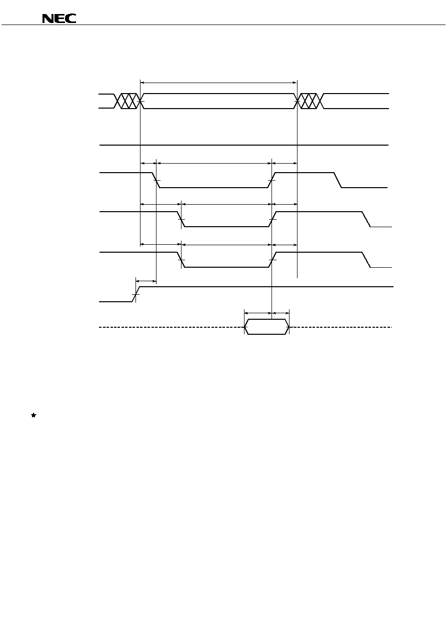
Preliminary Data Sheet M17507EJ2V0DS
43
PD46128512-X
Figure 7-11. Asynchronous Write Cycle Timing Chart 1 (Basic Timing1)
/CE1 (Input)
Address (Input)
DQ (Input)
High-Z
High-Z
t
WC
/WE (Input)
t
CW
t
WP
t
WR
/LB, /UB (Input)
L
/ADV (Input)
t
AS
t
AS
/OE (Input)
t
OES
t
WR
t
WR
t
BW
t
AS
t
DW
t
DH
A1
Data In D1
Cautions 1. During address transition, at least one of pins /CE1 and /WE, or both of /LB and /UB pins should
be inactivated.
2. Do not input data to the DQ pins while they are in the output state.
3. In write cycle, CE2 and /OE should be fixed HIGH.
4. CLK should be fixed HIGH or LOW.
Remark Write operation is done during the overlap time of LOW of following signals.
∑ /CE1
∑ /WE
∑ /LB and/or /UB
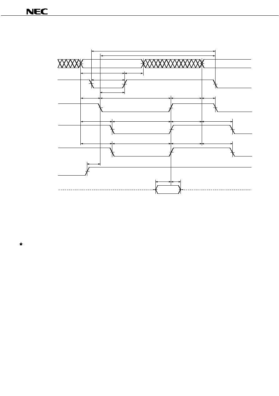
Preliminary Data Sheet M17507EJ2V0DS
44
PD46128512-X
Figure 7-12. Asynchronous Write Cycle Timing Chart 2 (Basic Timing2)
/CE1 (Input)
Address (Input)
DQ (Input)
High-Z
High-Z
t
WC
/WE (Input)
t
CW
t
WR
/LB, /UB (Input)
/ADV (Input)
t
ASC
/OE (Input)
t
OES
t
WR
t
BW
t
AS
t
DW
t
DH
t
WC
t
ASV
t
AH
t
VPL
t
VPL
t
AS
t
AS
t
WR
t
WP
t
AS
t
AS
Data In D1
A1
A2
Cautions 1. During address transition, at least one of pins /CE1 and /WE, or both of /LB and /UB pins should
be inactivated.
2. Do not input data to the DQ pins while they are in the output state.
3. In write cycle, CE2 and /OE should be fixed HIGH.
4. CLK should be fixed HIGH or LOW.
Remark Write operation is done during the overlap time of LOW of following signals.
∑ /CE1
∑ /WE
∑ /LB and/or /UB
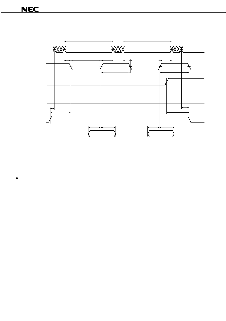
Preliminary Data Sheet M17507EJ2V0DS
45
PD46128512-X
Figure 7-13. Asynchronous Write Cycle Timing Chart 3 (/CE1 Controlled)
t
WC
t
AS
t
WC
t
AS
A1
A2
A3
t
CW
t
CW
t
WR
t
WR
t
CP
t
CP
/CE1 (Input)
Address (Input)
/WE (Input)
/LB, /UB (Input)
Data In D2
Data In D1
t
DW
t
DH
t
DW
t
DH
/OE (Input)
t
ASO
t
OHAH
t
OES
DQ (Input)
High-Z
High-Z
High-Z
L
L
t
OEH
Cautions 1. During address transition, at least one of pins /CE1 and /WE, or both of /LB and /UB pins should
be inactivated.
2. Do not input data to the DQ pins while they are in the output state.
3. In write cycle, CE2 and /OE should be fixed HIGH.
4. /ADV should be fixed LOW or toggled HIGH
LOW HIGH. CLK should be fixed HIGH or LOW.
Remark Write operation is done during the overlap time of LOW of following signals.
∑ /CE1
∑ /WE
∑ /LB and/or /UB
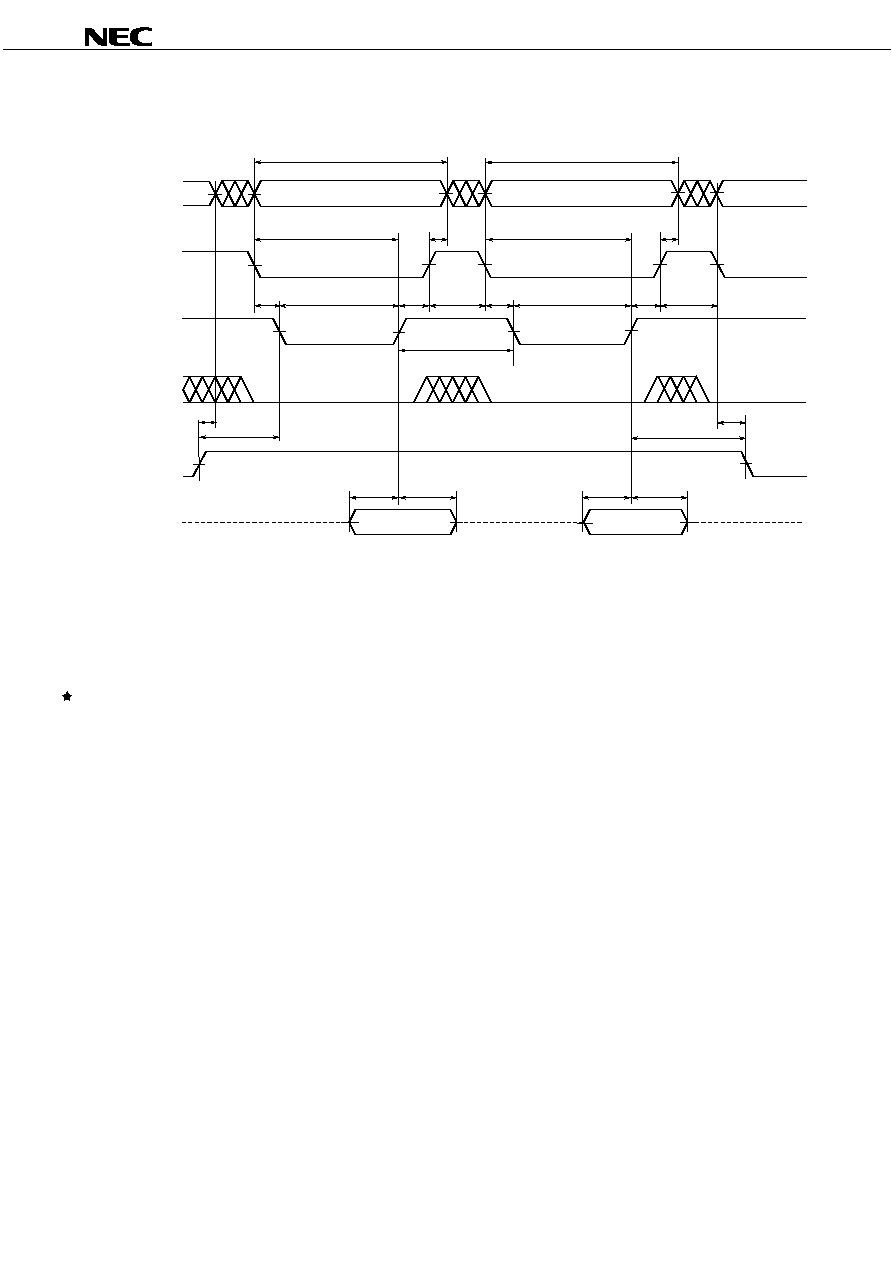
Preliminary Data Sheet M17507EJ2V0DS
46
PD46128512-X
Figure 7-14. Asynchronous Write Cycle Timing Chart 4 (/WE Controlled)
t
WC
t
AS
t
WC
t
AS
t
WHP
A1
A2
A3
t
CW
t
WHCH
t
CW
t
DW
t
DH
t
DW
t
DH
t
WP
t
WP
/OE (Input)
t
CP
t
ASO
t
OHAH
t
OES
t
OEH
t
WHCH
t
CP
t
CHAH
t
CHAH
/CE1 (Input)
Address (Input)
DQ (Input)
High-Z
High-Z
High-Z
/WE (Input)
/LB, /UB (Input)
Data In D2
Data In D1
Cautions 1. During address transition, at least one of pins /CE1 and /WE, or both of /LB and /UB pins should
be inactivated.
2. Do not input data to the DQ pins while they are in the output state.
3. In write cycle, CE2 and /OE should be fixed HIGH.
4. /ADV should be fixed LOW or toggled HIGH
LOW HIGH. CLK should be fixed HIGH or LOW.
Remark Write operation is done during the overlap time of LOW of following signals.
∑ /CE1
∑ /WE
∑ /LB and/or /UB

Preliminary Data Sheet M17507EJ2V0DS
47
PD46128512-X
Figure 7-15. Asynchronous Write Cycle Timing Chart 5 (/WE Controlled)
t
WC
t
AS
t
WC
t
AS
t
ASO
A1
A2
A3
t
WR
t
WR
/OE (Input)
t
OHAH
t
OES
t
OEH
t
WHP1
t
AW
t
AW
t
DW
t
DH
t
DW
t
DH
t
WP
t
WP
/CE1 (Input)
Address (Input)
DQ (Input)
High-Z
High-Z
High-Z
/WE (Input)
/LB, /UB (Input)
L
Data In D2
Data In D1
Cautions 1. During address transition, at least one of pins /CE1 and /WE, or both of /LB and /UB pins should
be inactivated.
2. Do not input data to the DQ pins while they are in the output state.
3. In write cycle, CE2 and /OE should be fixed HIGH.
4. /ADV should be fixed LOW or toggled HIGH
LOW HIGH. CLK should be fixed HIGH or LOW.
Remark Write operation is done during the overlap time of LOW of following signals.
∑ /CE1
∑ /WE
∑ /LB and/or /UB

Preliminary Data Sheet M17507EJ2V0DS
48
PD46128512-X
Figure 7-16. Asynchronous Write Cycle Timing Chart 6 (/LB, /UB Controlled)
t
WC
t
AS
t
WC
t
AS
A1
A2
A3
t
WR
t
WR
t
DW
t
DH
t
DW
t
DH
t
BW
t
BW
t
BP
t
BP
t
ASO
/OE (Input)
t
OHAH
t
OES
t
OEH
/CE1 (Input)
Address (Input)
DQ (Input)
High-Z
High-Z
High-Z
/WE (Input)
/LB, /UB (Input)
L
Data In D2
Data In D1
Cautions 1. During address transition, at least one of pins /CE1 and /WE, or both of /LB and /UB pins should
be inactivated.
2. Do not input data to the DQ pins while they are in the output state.
3. In write cycle, CE2 and /OE should be fixed HIGH.
4. /ADV should be fixed LOW or toggled HIGH
LOW HIGH. CLK should be fixed HIGH or LOW.
Remark Write operation is done during the overlap time of LOW of following signals.
∑ /CE1
∑ /WE
∑ /LB and/or /UB
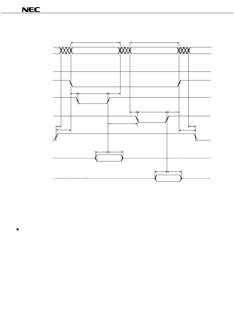
Preliminary Data Sheet M17507EJ2V0DS
49
PD46128512-X
Figure 7-17. Asynchronous Write Cycle Timing Chart 7 (/LB, /UB Independent Controlled 1)
t
WC
t
AS
t
WC
t
AS
A1
A2
A3
t
WR
t
WR
t
DW
t
DH
t
DW
t
DH
t
BW
t
BW
t
ASO
/OE (Input)
t
OHAH
t
OES
t
OEH
t
BP
/CE1 (Input)
Address (Input)
DQ0 to DQ7 (Input)
High-Z
High-Z
High-Z
High-Z
/WE (Input)
/LB (Input)
/UB (Input)
DQ8 to DQ15 (Input)
L
Data In D2
Data In D1
Cautions 1. During address transition, at least one of pins /CE1 and /WE, or both of /LB and /UB pins should
be inactivated.
2. Do not input data to the DQ pins while they are in the output state.
3. In write cycle, CE2 and /OE should be fixed HIGH.
4. /ADV should be fixed LOW or toggled HIGH
LOW HIGH. CLK should be fixed HIGH or LOW.
Remark Write operation is done during the overlap time of LOW of following signals.
∑ /CE1
∑ /WE
∑ /LB and/or /UB

Preliminary Data Sheet M17507EJ2V0DS
50
PD46128512-X
Figure 7-18. Asynchronous Write Cycle Timing Chart 8 (/LB, /UB Independent Controlled 2)
High-Z
High-Z
High-Z
High-Z
t
WC
t
AS
t
WC
t
AS
A1
A2
A3
t
WR
t
WR
t
DW
t
DH
t
DW
t
DH
t
WP
t
BW
t
ASO
t
OHAH
t
OES
t
OEH
t
BP
t
BS
t
BH
/CE1 (Input)
Address (Input)
DQ0 to DQ7 (Input)
/WE (Input)
/LB (Input)
/UB (Input)
DQ8 to DQ15 (Input)
/OE (Input)
L
Data In D2
Data In D1
Cautions 1. During address transition, at least one of pins /CE1 and /WE, or both of /LB and /UB pins should
be inactivated.
2. Do not input data to the DQ pins while they are in the output state.
3. In write cycle, CE2 and /OE should be fixed HIGH.
4. /ADV should be fixed LOW or toggled HIGH
LOW HIGH. CLK should be fixed HIGH or LOW.
Remark Write operation is done during the overlap time of LOW of following signals.
∑ /CE1
∑ /WE
∑ /LB and/or /UB

Preliminary Data Sheet M17507EJ2V0DS
51
PD46128512-X
Figure 7-19. Asynchronous Write Cycle Timing Chart 9 (/LB, /UB Independent Controlled 3)
High-Z
High-Z
High-Z
High-Z
t
WC
t
AS
t
WC
A1
A2
A3
t
WR
t
DW
t
DH
t
DW
t
DH
t
WP
t
ASO
t
OHAH
t
OES
t
OEH
t
AS
t
WR
t
WHP1
t
WP
t
BS
t
BH
t
BH
t
BS
/CE1 (Input)
Address (Input)
DQ0 to DQ7 (Input)
/WE (Input)
/LB (Input)
/UB (Input)
DQ8 to DQ15 (Input)
/OE (Input)
L
Data In D2
Data In D1
Cautions 1. During address transition, at least one of pins /CE1 and /WE, or both of /LB and /UB pins should
be inactivated.
2. Do not input data to the DQ pins while they are in the output state.
3. In write cycle, CE2 and /OE should be fixed HIGH.
4. /ADV should be fixed LOW or toggled HIGH
LOW HIGH. CLK should be fixed HIGH or LOW.
Remark Write operation is done during the overlap time of LOW of following signals.
∑ /CE1
∑ /WE
∑ /LB and/or /UB
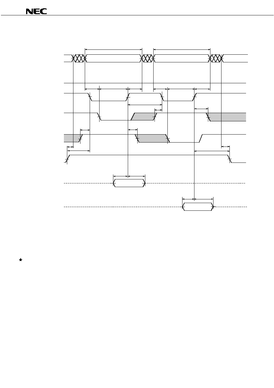
Preliminary Data Sheet M17507EJ2V0DS
52
PD46128512-X
Figure 7-20. Asynchronous Write Cycle Timing Chart 10 (/LB, /UB Independent Controlled 4)
High-Z
High-Z
High-Z
High-Z
t
WC
t
AS
t
WC
A1
A2
A3
t
WR
t
DW
t
DH
t
DW
t
DH
t
BW
t
ASO
t
OHAH
t
OES
t
OEH
t
AS
t
WR
t
WHP1
t
BW
t
BH
t
BH
t
BS
/CE1 (Input)
Address (Input)
DQ0 to DQ7 (Input)
/WE (Input)
/LB (Input)
/UB (Input)
DQ8 to DQ15 (Input)
/OE (Input)
t
BS
L
Data In D2
Data In D1
Cautions 1. During address transition, at least one of pins /CE1 and /WE, or both of /LB and /UB pins should
be inactivated.
2. Do not input data to the DQ pins while they are in the output state.
3. In write cycle, CE2 and /OE should be fixed HIGH.
4. /ADV should be fixed LOW or toggled HIGH
LOW HIGH. CLK should be fixed HIGH or LOW.
Remark Write operation is done during the overlap time of LOW of following signals.
∑ /CE1
∑ /WE
∑ /LB and/or /UB

Preliminary Data Sheet M17507EJ2V0DS
53
PD46128512-X
Figure 7-21. Asynchronous Write Cycle Timing Chart 11 (/LB, /UB Independent Controlled 5)
High-Z
High-Z
High-Z
High-Z
t
WC
t
AS
t
WC
A1
A2
A3
t
WR
t
DW
t
DH
t
DW
t
DH
t
BW
t
ASO
t
OHAH
t
OES
t
OEH
t
AS
t
WR
t
WHP1
t
BW
t
BS
t
BH
t
BH
t
BS
/CE1 (Input)
Address (Input)
DQ0 to DQ7 (Input)
/WE (Input)
/LB (Input)
/UB (Input)
DQ8 to DQ15 (Input)
/OE (Input)
L
Data In D2
Data In D1
Cautions 1. During address transition, at least one of pins /CE1 and /WE, or both of /LB and /UB pins should
be inactivated.
2. Do not input data to the DQ pins while they are in the output state.
3. In write cycle, CE2 and /OE should be fixed HIGH.
4. /ADV should be fixed LOW or toggled HIGH
LOW HIGH. CLK should be fixed HIGH or LOW.
Remark Write operation is done during the overlap time of LOW of following signals.
∑ /CE1
∑ /WE
∑ /LB and/or /UB
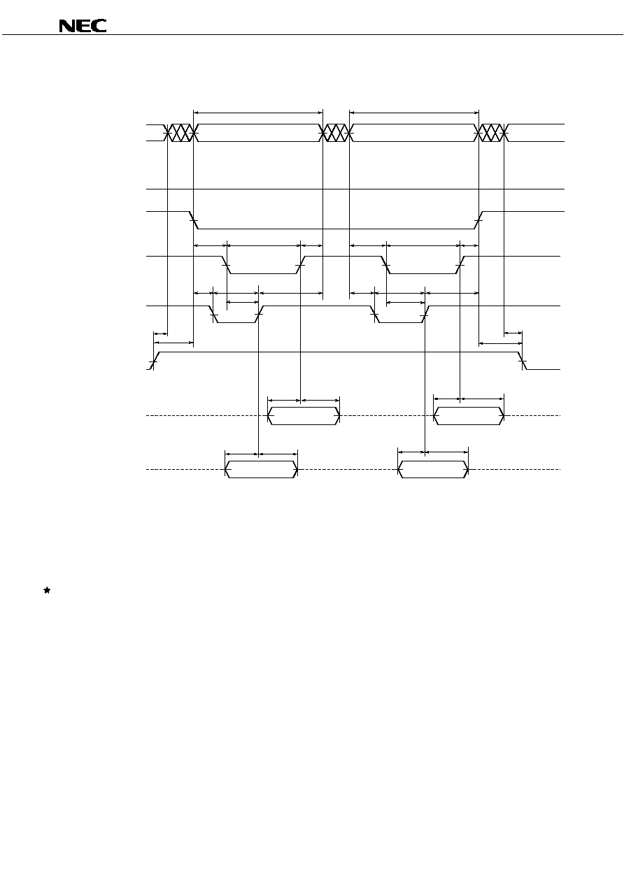
Preliminary Data Sheet M17507EJ2V0DS
54
PD46128512-X
Figure 7-22. Asynchronous Write Cycle Timing Chart 12 (/LB, /UB Independent Controlled 6)
High-Z
High-Z
High-Z
High-Z
t
WC
t
AS
t
WC
A1
A2
A3
t
WR
t
DW
t
DH
t
DW
t
DH
t
BW
t
ASO
t
OHAH
t
OES
t
OEH
t
AS
t
WR
t
BW
t
DW
t
DH
t
DW
t
DH
t
BW
t
AS
t
WR
t
BWO
t
BW
t
AS
t
WR
t
BWO
/CE1 (Input)
Address (Input)
DQ0 to DQ7 (Input)
/WE (Input)
/LB (Input)
/UB (Input)
DQ8 to DQ15 (Input)
/OE (Input)
L
Data In D2
Data In D1
Data In D2
Data In D1
Cautions 1. During address transition, at least one of pins /CE1 and /WE, or both of /LB and /UB pins should
be inactivated.
2. Do not input data to the DQ pins while they are in the output state.
3. In write cycle, CE2 and /OE should be fixed HIGH.
4. /ADV should be fixed LOW or toggled HIGH
LOW HIGH. CLK should be fixed HIGH or LOW.
Remark Write operation is done during the overlap time of LOW of following signals.
∑ /CE1
∑ /WE
∑ /LB and/or /UB

Preliminary Data Sheet M17507EJ2V0DS
55
PD46128512-X
Figure 7-23. Asynchronous Write-Read Cycle Timing Chart
/CE1 (Input)
Address (Input)
DQ (Input/Output)
High-Z
High-Z
High-Z
t
WC
/OE (Input)
t
AS
A1
/LB, /UB (Input)
/WE (Input)
t
AS
t
AS
t
CW
t
RC
t
RC
t
CHZ
t
OHZ
t
BHZ
t
OLZ
t
OE
t
WP
t
BW
t
OEH
t
DW
t
DH
t
AA
Data Out Q1
Data In D1
Cautions 1. During address transition, at least one of pins /CE1 and /WE, or both of /LB and /UB pins should
be inactivated.
2. Do not input data to the DQ pins while they are in the output state.
3. In write cycle, CE2 and /OE should be fixed HIGH.
4. /ADV should be fixed LOW or toggled HIGH
LOW HIGH. CLK should be fixed HIGH or LOW.
Remark Write operation is done during the overlap time of LOW of following signals.
∑ /CE1
∑ /WE
∑ /LB and/or /UB

Preliminary Data Sheet M17507EJ2V0DS
56
PD46128512-X
Figure 7-24. Asynchronous Read-Write Cycle Timing Chart
/CE1 (Input)
Address (Input)
DQ (Input/Output)
High-Z
High-Z
High-Z
t
RC
/OE (Input)
t
AA
A1
/LB, /UB (Input)
/WE (Input)
t
ASO
t
ACE
t
WC
t
CW
t
WR
t
OES
t
WR
t
OLZ
t
OE
t
WP
t
BA
t
DW
t
DH
t
RC
t
CLZ
t
BLZ
t
OHZ
t
WR
t
BW
Data Out Q1
Data In D1
Cautions 1. During address transition, at least one of pins /CE1 and /WE, or both of /LB and /UB pins should
be inactivated.
2. Do not input data to the DQ pins while they are in the output state.
3. In write cycle, CE2 and /OE should be fixed HIGH.
4. /ADV should be fixed LOW or toggled HIGH
LOW HIGH. CLK should be fixed HIGH or LOW.
Remark Write operation is done during the overlap time of LOW of following signals.
∑ /CE1
∑ /WE
∑ /LB and/or /UB

Preliminary Data Sheet M17507EJ2V0DS
57
PD46128512-X
8. Synchronous AC Specification, Timing Chart
Synchronous Read / Write Common Specification
Parameter Symbol
-E9X,
-E10X
-E11X, -E12X
Unit Note
MIN. MAX. MIN. MAX.
Clock Specifications
Cycle frequency
t
CYCLE
0.1 108 0.1 83
MHz
1
CLK HIGH width
t
CH
3 3
ns
CLK LOW width
t
CL
3 3
ns
CLK rise / fall time
t
CHCL
3 3
ns
Address Latching Specifications
Address setup time to CLK
t
ACS
5 5
ns
Address hold time to CLK
t
ACH
4 4
ns
/ADV setup time to CLK
t
CSV
5 10,000 5 10,000
ns
/ADV hold time from CLK
t
CHV
1 1
ns
/ADV = LOW pulse width
t
VPL
7 7
ns
Address hold time from /ADV = HIGH
t
AH
3 3
ns
/CE1 setup time to CLK
t
CES
5 5
ns
Asynchronous Specification
/CE1 to output in low impedance
t
CLZ
10 10
ns
2
/OE to output in low impedance
t
OLZ
5 5
ns
/LB, /UB to output in low impedance
t
BLZ
5 5
ns
/CE1 to output in high impedance
t
CHZ
9 9
ns
/OE to output in high impedance
t
OHZ
9 9
ns
/LB, /UB to output in high impedance
t
BHZ
9 9
ns
/WAIT Specification
/WAIT output time from /CE1 = LOW
t
CEWA
10 13
ns
3
/WAIT output time from /ADV = LOW
t
ADWA
10 13
ns
/WAIT = HIGH output time from CLK
t
CLWA
7 8
ns
/WAIT in high impedance from /CE1 = HIGH
t
CWHZ
10 10
ns
2
Others
/CE1 hold time
t
CEH
1 1
ns
/LB, /UB hold time
t
LUH
1 1
ns
/CE1 HIGH pulse width
t
CP
10 10
ns
Notes 1. Case BL (Burst Length) = Continuous : 2 MHz (MIN.)
2.
Output load: 5 pF
3.
Output load: 30 pF

Preliminary Data Sheet M17507EJ2V0DS
58
PD46128512-X
Synchronous Burst Read Cycle
Parameter Symbol
-E9X,
-E10X
-E11X, -E12X
Unit Note
MIN. MAX. MIN. MAX.
Synchronous Read Specifications
Burst access time
t
BACC
7 8
ns
1
Output data hold time
t
BDH
2 2
ns
/OE setup time to CLK for data output
t
OC
30 30
ns
/LB, /UB setup time to CLK for data output
t
BC
30 30
ns
/OE setup time for burst read suspend
t
SOES
5 5
ns
/OE hold time for burst read suspend
t
SOEH
1 1
ns
Burst read suspend time (/OE = HIGH)
t
SOP
9
10,000
12
10,000
ns
Burst read termination recovery time
t
TRB
18 24
ns
Note1.
Output load: 30 pF
Synchronous Burst Write Cycle
Parameter Symbol
-E9X,
-E10X
-E11X, -E12X
Unit Note
MIN. MAX. MIN. MAX.
Synchronous Write Specifications
/LB, /UB setup time to CLK
t
BC
30 30
ns
for latching data
/WE setup time for CLK
t
WES
5 5
ns
(In /WE single clock control operation)
(In burst write suspend operation)
/WE hold time in the write operation
t
WEH
1 1
ns
(In /WE single clock control operation)
(In burst write suspend operation)
Write data setup time
t
WDS
5 5
ns
Write data hold time
t
WDH
1 1
ns
/WE HIGH pulse width
t
SWHP
9
10,000
12
10,000
ns
/ADV LOW from CLK for latching the latest
data
t
WRB
2 2
CLK
Burst write termination recovery time
t
TRB
18 24
ns

Preliminary Data Sheet M17507EJ2V0DS
59
PD46128512-X
Figure 8-1. Synchronous CLK Input Timing Chart
CLK (Input)
t
CL
t
CH
t
CHCL
V
IH
V
IL
t
CYCLE
Figure 8-2. Synchronous Burst Read Cycle Timing Chart (/CE1 Control)
T0
T1
T2
T3
T4
T5
T6
Tm
Tn
T0
T1
T2
T3
T4
CLK (Input)
/ADV (Input)
Address (Input)
/CE1 (Input)
/WAIT (Output)
/OE (Input)
DQ (Output)
/LB, /UB (Input)
/WE (Input)
t
CH
t
CL
Q0
t
ACS
t
BACC
t
BDH
t
CEWA
t
CLWA
t
CSV
t
VPL
t
CHCL
t
CHCL
t
CLZ
t
ACS
t
CSV
t
VPL
t
CWHZ
t
CES
t
CES
t
ACH
t
ACH
t
CHV
t
AH
t
CHV
t
AH
RL = 5
t
CHV
t
CHV
t
CEH
t
CYCLE
Q1
Q
BL
High-Z
High-Z
Valid
High-Z
High-Z
t
BDH
H
t
CP
t
CEWA
t
CLZ
Valid
L
L
t
CHZ
Remarks 1. The above timing chart assumes Read Latency is 5 and Burst Length is 8 or 16.
Q
BL
means the latest data out of burst length.
2.
CE2 should be fixed HIGH.
3.
Valid clock edge is the rising edge.
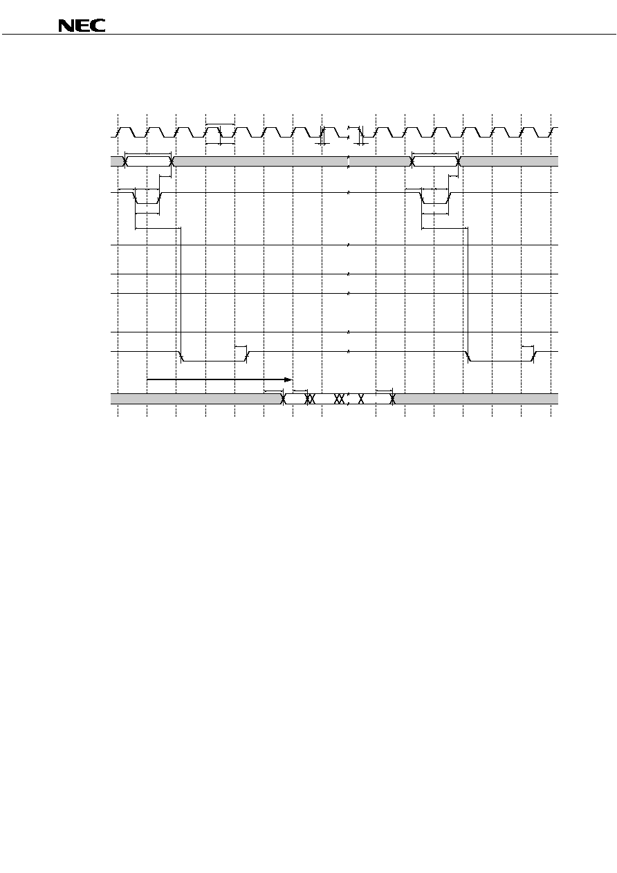
Preliminary Data Sheet M17507EJ2V0DS
60
PD46128512-X
Figure 8-3. Synchronous Burst Read Cycle Timing Chart (/ADV Control)
T0
T1
T2
T3
T4
T5
T6
Tm
Tn
T0
T1
T2
T3
T4
CLK (Input)
/ADV (Input)
Address (Input)
/CE1 (Input)
/WAIT (Output)
/OE (Input)
DQ (Output)
/LB, /UB (Input)
/WE (Input)
t
CH
t
CL
Q0
t
ACS
t
BACC
t
BDH
t
CLWA
t
CLWA
t
CSV
t
VPL
t
CHCL
t
CHCL
t
ACS
t
CSV
t
VPL
t
ACH
t
ACH
t
CHV
t
AH
t
CHV
t
AH
RL = 5
t
CHV
t
CHV
t
CYCLE
Q1
Valid
t
BDH
H
t
ADWA
t
ADWA
Valid
L
L
L
Q
BL
Remarks 1. The above timing chart assumes Read Latency is 5 and Burst Length is 8 or 16.
Q
BL
means the latest data out of burst length.
2.
CE2 should be fixed HIGH.
3.
Valid clock edge is the rising edge.
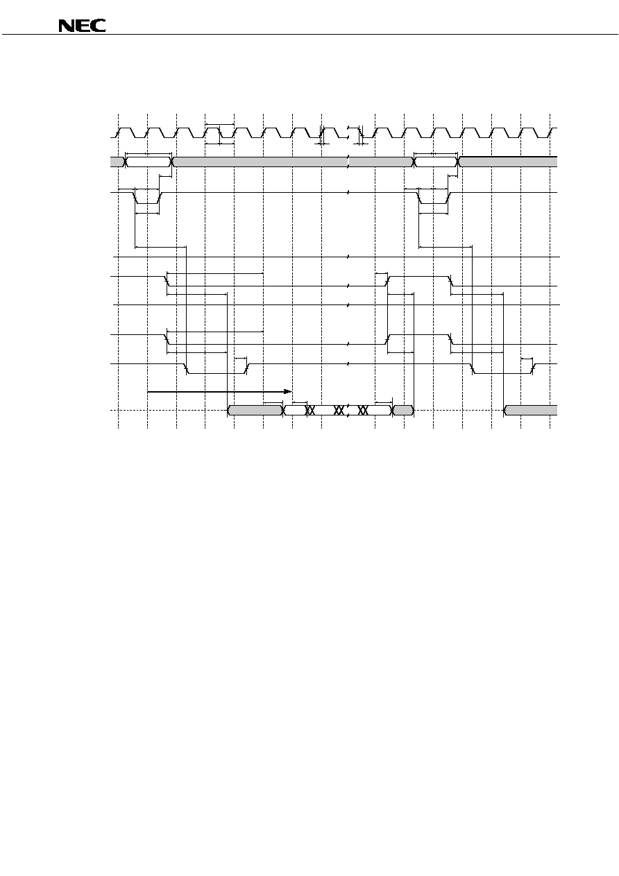
Preliminary Data Sheet M17507EJ2V0DS
61
PD46128512-X
Figure 8-4. Synchronous Burst Read Cycle Timing Chart (/OE Control)
T0
T1
T2
T3
T4
T5
T6
Tm
Tn
T0
T1
T2
T3
T4
t
CLWA
CLK (Input)
/ADV (Input)
Address (Input)
/CE1 (Input)
/WAIT (Output)
/OE (Input)
DQ (Output)
/LB, /UB (Input)
/WE (Input)
t
CH
t
CL
Q0
t
ACS
t
BACC
t
BDH
t
ADWA
t
ADWA
t
BLZ
t
BC
t
OLZ
t
BLZ
t
OLZ
t
OC
t
CLWA
t
CSV
t
VPL
t
CHCL
t
CHCL
t
ACS
t
CSV
t
VPL
t
ACH
t
ACH
t
CHV
t
AH
t
CHV
t
AH
RL = 5
t
CHV
t
CHV
t
SOEH
t
CYCLE
Q1
Q
BL
High-Z
Valid
High-Z
t
BDH
H
Valid
L
t
BHZ
t
OHZ
Remarks 1. The above timing chart assumes Read Latency is 5 and Burst Length is 8 or 16.
Q
BL
means the latest data out of burst length.
2. CE2 should be fixed HIGH.
3. Valid clock edge is the rising edge.
4. t
OC
and t
BC
are defined from CLK rising edge of RL
-1 to /OE = LOW, /LB and /UB = LOW.

Preliminary Data Sheet M17507EJ2V0DS
62
PD46128512-X
Figure 8-5. Synchronous Burst /WAIT Timing Chart (Continuous)
T0
T1
T2
T3
T4
T5
T6
T8
T7
T9
T10
T11
T12
CLK (Input)
/ADV (Input)
Address (Input)
/CE1 (Input)
/WAIT (Output)
/OE (Input)
DQ (Output)
/LB, /UB (Input)
/WE (Input)
t
CH
t
CL
Qmf
t
ACS
t
BACC
t
BDH
t
CEWA
t
CLWA
t
CLWA
t
CLWA
t
CSV
t
VPL
t
CHCL
t
CHCL
t
CLZ
t
OC
t
BC
t
OLZ
t
BLZ
t
CES
t
ACH
t
CHV
t
AH
RL = 5
t
CHV
t
CYCLE
Qn0
Qn1
High-Z
High-Z
ADDmf
H
Remarks 1. The above timing chart assumes Burst length is continuous.
2. CE2 should be fixed HIGH.
3. Valid clock edge is the rising edge.
4. t
OC
and t
BC
are defined from CLK rising edge of RL
-1 to /OE = LOW, /LB and /UB = LOW.
5. The above timing chart assumes Read Latency is 5 and start address is from xxxfH and the number of
dummy wait cycles are 5 cycles.
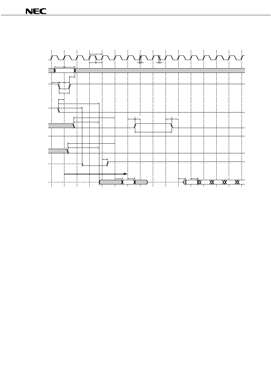
Preliminary Data Sheet M17507EJ2V0DS
63
PD46128512-X
Figure 8-6. Synchronous Burst Read Suspend Timing Chart
T0
T1
T2
T3
T4
T5
T6
T7
T8
T9
T10
CLK (Input)
/ADV (Input)
Address (Input)
/CE1 (Input)
/WAIT (Output)
/OE (Input)
DQ (Output)
/LB, /UB (Input)
/WE (Input)
t
CH
t
CL
Q0
t
ACS
t
BACC
t
BDH
t
BACC
t
BDH
t
CEWA
t
CLWA
t
CSV
t
VPL
t
CHCL
t
CHCL
t
CLZ
t
OLZ
t
OC
t
BLZ
t
BC
t
SOP
t
CES
t
ACH
t
CHV
t
AH
RL = 5
t
CHV
t
CYCLE
Q1
Q2
Q3
Q4
High-Z
High-Z
Valid
High-Z
H
t
SOEH
t
SOES
t
SOEH
t
SOES
Remarks 1. The above timing chart assumes Read Latency is 5 and Burst Length is 8 or 16.
2. CE2 should be fixed HIGH.
3. Valid clock edge is the rising edge.
4. t
OC
and t
BC
are defined from CLK rising edge of RL
-1 to /OE = LOW, /LB and /UB = LOW.
5. Burst read suspend is valid after outputting the first read access data (Q0).

Preliminary Data Sheet M17507EJ2V0DS
64
PD46128512-X
Figure 8-7. Synchronous Burst Read Termination Cycle Timing Chart
T0
T1
T2
T3
T4
T0
T1
T2
T3
T4
CLK (Input)
/ADV (Input)
Address (Input)
/CE1 (Input)
/WAIT (Output)
/OE (Input)
DQ (Output)
/LB, /UB (Input)
/WE (Input)
t
CH
t
CL
Q0
t
ACS
t
BACC
t
CLWA
t
CSV
t
VPL
t
CHCL
t
CHCL
t
ACS
t
CSV
t
VPL
t
CES
t
CES
t
ACH
t
ACH
t
CHV
t
AH
t
CHV
t
AH
RL = 5
t
CHV
t
TRB
t
CHV
t
CEH
t
CYCLE
High-Z
High-Z
Valid
High-Z
High-Z
t
BDH
H
t
CEWA
t
CLZ
t
CES
t
CEWA
t
CLZ
t
OLZ
t
OC
t
BLZ
t
BC
Valid
t
CWHZ
t
CHZ
Remarks 1. The above timing chart assumes Read Latency is 5.
2. CE2 should be fixed HIGH.
3. Valid clock edge is the rising edge.
4. t
OC
and t
BC
are defined from CLK rising edge of RL
-1 to /OE = LOW, /LB and /UB = LOW.
5. t
TRB
is specified from /CE1 de-assert to /CE1 assert for next operation.
6. Burst read termination is valid after outputting the first read access data (Q0).
7. In case continuous burst read is set, /CE1 de-assert is needed for burst read termination.

Preliminary Data Sheet M17507EJ2V0DS
65
PD46128512-X
Figure 8-8. Synchronous Burst Write Cycle Timing Chart (/WE Level Control)
T0
T1
T2
T3
T4
T5
Tl
Tm
Tn
T0
T1
CLK (Input)
/ADV (Input)
Address (Input)
/CE1 (Input)
/WAIT (Output)
/OE (Input)
DQ (Input)
/LB, /UB (Input)
/WE (Input)
t
CH
t
CL
D0
t
ACS
t
WDS
t
WDH
t
CEWA
t
CEWA
t
BC
t
WES
t
CLWA
t
CSV
t
CES
t
VPL
t
ACS
t
CSV
t
VPL
t
ACH
t
ACH
t
CHV
t
AH
t
CHV
t
AH
RL = 5
t
CHV
t
CHV
t
WRB
t
LUH
t
WEH
t
CEH
t
CEH
t
CES
t
CYCLE
D1
D
BL
High-Z
High-Z
H
Valid
High-Z
High-Z
Valid
t
CWHZ
Remarks 1. The above timing chart assumes Read Latency is 5 and Burst Length is 8 or 16.
D
BL
means the latest data input of burst length.
2. CE2 should be fixed HIGH.
3. Valid clock edge is the rising edge.
4. t
BC
is defined from CLK rising edge of RL
-1 to /LB and /UB = LOW.

Preliminary Data Sheet M17507EJ2V0DS
66
PD46128512-X
Figure 8-9. Synchronous Burst Write Cycle Timing Chart (/WE Single Clock Control)
T0
T1
T2
T3
T4
T5
Tl
Tm
Tn
T0
T1
CLK (Input)
/ADV (Input)
Address (Input)
/CE1 (Input)
/WAIT (Output)
/OE (Input)
DQ (Input)
/LB, /UB (Input)
/WE (Input)
t
CH
t
CL
D0
t
ACS
t
WDS
t
WDH
t
CEWA
t
CEWA
t
BC
t
WES
t
CLWA
t
CSV
t
CES
t
VPL
t
ACS
t
CSV
t
VPL
t
ACH
t
ACH
t
CHV
t
AH
t
CHV
t
AH
RL = 5
t
CHV
t
CHV
t
WRB
t
LUH
t
WEH
t
WES
t
WEH
t
CEH
t
CEH
t
CES
t
CYCLE
D1
D
BL
High-Z
High-Z
H
Valid
High-Z
High-Z
Valid
t
CWHZ
Remarks 1. The above timing chart assumes Read Latency is 5 and Burst Length is 8 or 16.
D
BL
means the latest data input of burst length.
2.
CE2 should be fixed HIGH.
3.
Valid clock edge is the rising edge.
4.
t
BC
is defined from CLK rising edge of RL
-1 to /LB and /UB = LOW.
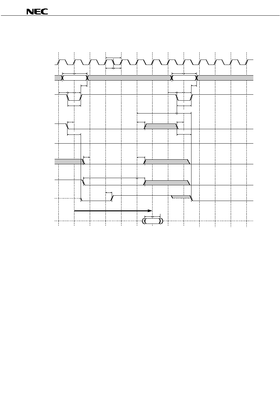
Preliminary Data Sheet M17507EJ2V0DS
67
PD46128512-X
Figure 8-10. Synchronous Single Write Cycle Timing Chart (/WE level Control)
T0
T1
T2
T3
T4
T0
T1
T2
T3
CLK (Input)
/ADV (Input)
Address (Input)
/CE1 (Input)
/WAIT (Output)
/OE (Input)
DQ (Input)
/LB, /UB (Input)
/WE (Input)
t
CH
t
CL
D0
t
ACS
t
CLWA
t
CSV
t
VPL
t
VPL
t
ACS
t
CSV
t
ADWA
t
WRB
t
ACH
t
ACH
t
CHV
t
AH
t
CHV
t
AH
RL = 5
t
CHV
t
CEWA
t
CHV
t
CYCLE
High-Z
H
High-Z
Valid
High-Z
t
WDH
t
WDS
t
CES
t
CES
t
WES
t
CEWA
t
LUH
t
WEH
t
BC
t
CEH
Valid
Remarks 1. The above timing chart assumes Read Latency is 5.
2. CE2 should be fixed HIGH.
3. Valid clock edge is the rising edge.
4.
t
BC
is defined from CLK rising edge of RL
-1 to /LB and /UB = LOW.

Preliminary Data Sheet M17507EJ2V0DS
68
PD46128512-X
Figure 8-11. Synchronous Burst Write Suspend Timing Chart
T0
T1
T2
T3
T4
T5
T6
T7
T8
T9
H
CLK (Input)
/ADV (Input)
Address (Input)
/CE1 (Input)
/WAIT (Output)
/OE (Input)
DQ (Input)
/LB, /UB (Input)
/WE (Input)
t
CH
t
CL
D0
t
ACS
t
WDS
t
WDH
t
WDS
t
WDH
t
CEWA
t
CLWA
t
CSV
t
VPL
t
CHCL
t
CHCL
t
BC
t
SWHP
t
CES
t
ACH
t
CHV
t
AH
RL = 5
t
CHV
t
CYCLE
D1
D2
D3
D4
High-Z
High-Z
Valid
High-Z
t
WEH
t
WES
t
WES
t
WEH
t
WES
Remarks 1. The above timing chart assumes Read Latency is 5.
2. CE2 should be fixed HIGH.
3. Valid clock edge is the rising edge.
4. t
BC
is defined from CLK rising edge of RL
-1 to /LB and /UB = LOW.
5. Burst write suspend is valid after latching the first write data
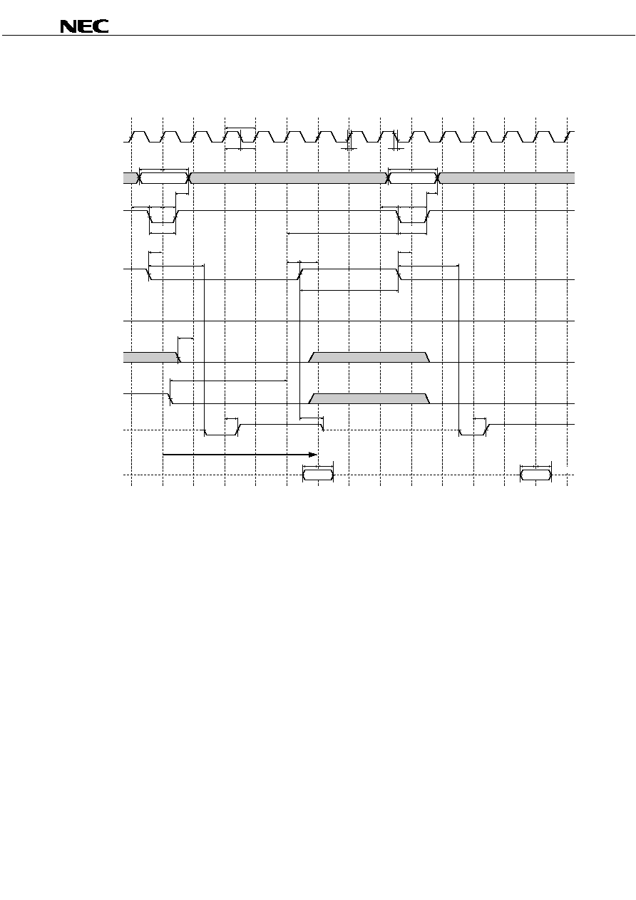
Preliminary Data Sheet M17507EJ2V0DS
69
PD46128512-X
Figure 8-12. Synchronous Burst Write Termination Timing Chart
T0
T1
T2
T3
T4
T0
T1
T2
T3
T4
CLK (Input)
/ADV (Input)
Address (Input)
/CE1 (Input)
/WAIT (Output)
/OE (Input)
DQ (Input/Output)
/LB, /UB (Input)
/WE (Input)
t
CH
t
CL
D0
t
ACS
t
CLWA
t
CLWA
t
CSV
t
VPL
t
CHCL
t
CHCL
t
ACS
t
CSV
t
VPL
t
WRB
t
CES
t
CES
t
ACH
t
ACH
t
CHV
t
AH
t
CHV
t
AH
RL = 5
t
CHV
t
TRB
t
CHV
t
CEH
t
CYCLE
High-Z
High-Z
Valid
High-Z
High-Z
t
WDH
t
WDS
D0
t
WDH
t
WDS
H
t
CEWA
t
CES
t
CEWA
t
BC
t
WES
Valid
t
CWHZ
High-Z
Remarks 1. The above timing chart assumes Read Latency is 5.
2. CE2 should be fixed HIGH.
3. Valid clock edge is the rising edge.
4. t
BC
is defined from CLK rising edge of RL
-1 to /LB and /UB = LOW.
5. Burst write suspend is valid after latching the first write data
6. In case continuous burst write is set, /CE1 de-assert is needed for burst write termination.
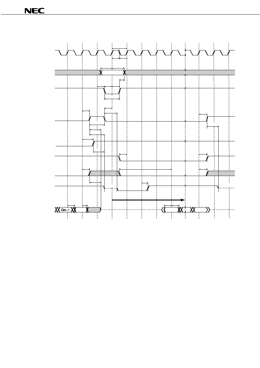
Preliminary Data Sheet M17507EJ2V0DS
70
PD46128512-X
Figure 8-13. Synchronous Burst Read ≠ Burst Write Cycle Timing Chart (/CE1 Control)
CLK (Input)
/ADV (Input)
Address (Input)
/CE1 (Input)
/WAIT (Output)
/OE (Input)
DQ (Input/Output)
/LB, /UB (Input)
/WE (Input)
t
CH
t
CL
D0
t
ACS
t
WDS
t
WDH
t
BACC
t
BDH
t
BC
t
LUH
t
BHZ
t
WES
t
CLWA
t
CSV
t
CES
t
CEH
t
SOEH
t
CHZ
t
ACH
t
CHV
t
AH
RL = 5
t
CHV
t
LUH
t
WEH
t
CEH
t
CYCLE
D
BL
Q
BL
High-Z
Valid
High-Z
t
CWHZ
t
VPL
t
CEWA
High-Z
t
CWHZ
t
OHZ
t
CP
High-Z
Remarks 1. The above timing chart assumes Read Latency is 5 and Burst Length is 8 or 16.
Q
BL
means the latest data out of burst length. D
BL
means the latest data input of burst length.
2. CE2 should be fixed HIGH.
3. Valid clock edge is the rising edge.
4. t
BC
is defined from CLK rising edge of RL
-1 to /LB and /UB = LOW.

Preliminary Data Sheet M17507EJ2V0DS
71
PD46128512-X
Figure 8-14. Synchronous Burst Read ≠ Burst Write Cycle Timing Chart (/ADV Control)
CLK (Input)
/ADV (Input)
Address (Input)
/CE1 (Input)
/WAIT (Output)
/OE (Input)
DQ (Input/Output)
/LB, /UB (Input)
/WE (Input)
t
CH
t
CL
D0
t
ACS
t
WDS
t
WDH
t
BACC
t
BDH
t
BC
t
LUH
t
BHZ
t
WES
t
CLWA
t
CSV
t
SOEH
t
ACH
t
CHV
t
AH
RL = 5
t
CHV
t
LUH
t
WEH
t
CYCLE
D
BL
Q
BL
High-Z
L
Valid
High-Z
t
VPL
t
OHZ
High-Z
t
ADWA
Remarks 1. The above timing chart assumes Read Latency is 5 and Burst Length is 8 or 16.
Q
BL
means the latest data out of burst length. D
BL
means the latest data input of burst length.
2. CE2 should be fixed HIGH.
3. Valid clock edge is the rising edge.
4. t
BC
is defined from CLK rising edge of RL
-1 to /LB and /UB = LOW.

Preliminary Data Sheet M17507EJ2V0DS
72
PD46128512-X
Figure 8-15. Synchronous Burst Write ≠ Burst Read Cycle Timing Chart (/CE1 Control)
CLK (Input)
/ADV (Input)
Address (Input)
/CE1 (Input)
/WAIT (Output)
/OE (Input)
DQ (Input/Output)
/LB, /UB (Input)
/WE (Input)
t
CH
t
CL
Q0
t
ACS
t
BACC
t
BDH
t
WDH
t
WDS
t
BC
t
OC
t
LUH
t
CLWA
t
CSV
t
CES
t
CEH
t
ACH
t
CHV
t
AH
RL = 5
t
CHV
t
WEH
t
CYCLE
D
BL
High-Z
Valid
t
VPL
t
WRB
t
CLZ
t
CEWA
High-Z
t
CWHZ
t
CP
t
BLZ
t
OLZ
Remarks 1. The above timing chart assumes Read Latency is 5 and Burst Length is 8 or 16.
D
BL
means the latest data input of burst length.
2. CE2 should be fixed HIGH.
3. Valid clock edge is the rising edge.
4. t
OC
and t
BC
are defined from CLK rising edge of RL
-1 to /OE = LOW, /LB and /UB = LOW.

Preliminary Data Sheet M17507EJ2V0DS
73
PD46128512-X
Figure 8-16. Synchronous Burst Write ≠ Burst Read Cycle Timing Chart (/ADV Control)
CLK (Input)
/ADV (Input)
Address (Input)
/CE1 (Input)
/WAIT (Output)
/OE (Input)
DQ (Input/Output)
/LB, /UB (Input)
/WE (Input)
t
CH
t
CL
Q0
t
ACS
t
BACC
t
BDH
t
WDH
t
WDS
t
BC
t
OC
t
LUH
t
CLWA
t
CSV
t
ACH
t
CHV
t
AH
RL = 5
t
CHV
t
WEH
t
CYCLE
D
BL
High-Z
L
Valid
t
VPL
t
WRB
t
OLZ
t
ADWA
t
BLZ
Remarks 1. The above timing chart assumes Read Latency is 5 and Burst Length is 8 or 16.
D
BL
means the latest data input of burst length.
2. CE2 should be fixed HIGH.
3. Valid clock edge is the rising edge.
4. t
OC
and t
BC
are defined from CLK rising edge of RL
-1 to /OE = LOW, /LB and /UB = LOW.

Preliminary Data Sheet M17507EJ2V0DS
74
PD46128512-X
9. Mode Register Setting Timing
Figure 9-1. Mode Register Setting Timing Chart (Asynchronous Timing + CLK fixed LOW/HIGH)
/LB, /UB (Input)
/WE (Input)
/CE1 (Input)
Address (Input)
/OE (Input)
DQ (Input/Output)
t
RC
t
WC
t
WC
7FFFFFH
t
WP
t
WR
t
WP
t
WR
t
DW
t
DH
t
DW
t
DH
7FFFFFH
7FFFFFH
7FFFFFH
Code1
Code2
High-Z
High-Z
High-Z
7FFFFFH
t
WC
t
WP
t
WR
t
DW
t
DH
t
WC
t
WP
t
WR
t
DW
t
DH
High-Z
t
RC
Don't care
High-Z
t
CE
t
OE
RDa
t
CE
t
OE
RDb
High-Z
High-Z
t
OHZ
t
CHZ
t
OHZ
t
CHZ
Don't care
Don't care
CLK (Input)
H
L
Remarks 1. For the data of Code1 and Code2, refer to Table 5-1. Mode Register Definition (4th Bus Cycle) and
Table 5-2. Mode Register Definition (5th Bus Cycle).
2. RDa and RDb are the output data.
3. /ADV fixed LOW or toggle HIGH
LOW HIGH.
Figure 9-2. Mode Register Setting Timing Chart (Asynchronous Timing + Toggle CLK)
/LB, /UB (Input)
/WE (Input)
/CE1 (Input)
Address (Input)
/OE (Input)
DQ (Input/Output)
t
RC
t
WC
t
WC
7FFFFFH
t
WP
t
WR
t
WP
t
WR
t
DW
t
DH
t
DW
t
DH
7FFFFFH
7FFFFFH
7FFFFFH
High-Z
High-Z
High-Z
7FFFFFH
t
WC
t
WP
t
WR
t
DW
t
DH
t
WC
t
WP
t
WR
t
DW
t
DH
High-Z
t
RC
High-Z
t
CE
t
OE
RDa
t
CE
t
OE
RDb
High-Z
High-Z
t
OHZ
t
CHZ
t
OHZ
t
CHZ
CLK (Input)
Code1
Code2
Don't care
Don't care
Don't care
Remarks 1. For the data of Code1 and Code2, refer to Table 5-1. Mode Register Definition (4th Bus Cycle) and
Table 5-2. Mode Register Definition (5th Bus Cycle).
2. RDa and RDb are the output data.
3. /ADV fixed LOW or toggle HIGH
LOW HIGH.

Preliminary Data Sheet M17507EJ2V0DS
75
PD46128512-X
Figure 9-3. Mode Register Setting Timing Chart (Synchronous Timing)
CLK (Input)
/CE1 (Input)
Address (Input)
/WE (Output)
/ADV (Input)
DQ (Input/Output)
/LB, /UB (Input)
/OE (Input)
*A
*A
*A
*A
*A
RDb
RDa
High-Z
High-Z
High-Z
High-Z
High-Z
High-Z
High-Z
High-Z
High-Z
High-Z
High-Z
High-Z
High-Z
Code1
Code2
Don't
care
Don't
care
Don't
care
Caution Refer to 8. Synchronous Read/Write specification.
Remarks 1. *A means the highest address (7FFFFFH).
2. For the data of Code1 and Code2, refer to Table 5-1. Mode Register Definition (4th Bus Cycle) and
Table 5-2. Mode Register Definition (5th Bus Cycle).
3. RDa and RDb are the output data.
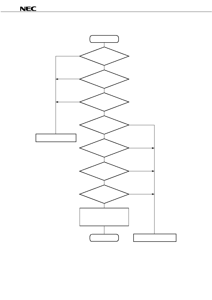
Preliminary Data Sheet M17507EJ2V0DS
76
PD46128512-X
Figure 9-4. Mode Register Setting Flow Chart
No
No
No
Yes
Yes
Yes
Yes
Yes
Yes
Yes
No
No
No
No
Start
Read Operation
Address = 7FFFFFH
toggled the
/CE1 and /OE
Write Operation
Address = 7FFFFFH
toggled the /CE1
Write Operation
Address = 7FFFFFH
toggled the /CE1
Write Operation
Address = 7FFFFFH
toggled the /CE1
Write Data = Code 1
Note1
Write Operation
Address = 7FFFFFH
toggled the /CE1
Write Data = Code 2
Note2
Read Operation
Address = Don't Care
toggled the /CE1 and /OE
End
Mode Register Setting Exit
Re-setup the mode register
Notes 1. Refer
to
Table 5-1.
2. Refer
to
Table 5-2.

Preliminary Data Sheet M17507EJ2V0DS
77
PD46128512-X
10. Standby Mode Timing Chart
Figure 10-1. Standby Mode 2 Entry / Exit Timing Chart (Asynchronous Mode)
/CE1 (Input)
t
CHML
t
MHCL
CE2 (Input)
Standby
Mode 1
Standby Mode 2
Figure 10-2. Standby Mode 2 Entry / Exit Timing Chart (Synchronous Mode)
/CE1 (Input)
t
MHCL
CE2 (Input)
t
CE2S
t
CES
t
CES
CLK (Input)
Standby
Mode 1
Standby Mode 2
Standby Mode 2 Entry / Exit
Parameter Symbol
MIN.
MAX.
Unit
Note
Standby mode 2 entry /CE1 HIGH to CE2 LOW
t
CHML
0
ns
Standby mode 2 exit to normal operation CE2 HIGH to /CE1 LOW
t
MHCL
30
ns
1
300
s 2
/CE1 = HIGH setup time to CLK
t
CES
5
ns
CE2 = LOW hold time to CLK
t
CE2S
1
ns
Notes 1. This is the time it takes to return to normal operation from Standby Mode 2 (data hold: 32M bits / 16M bits /
8M bits).
2. This is the time it takes to return to normal operation from Standby Mode 2 (data not held).

Preliminary Data Sheet M17507EJ2V0DS
78
PD46128512-X
11. Package Drawing
The following is a package drawing of package sample.
A
S
B
10
9
8
7
6
5
4
3
2
1
C B A
D
E
F
G
H
J
K
L
M
N
P
ZD
ZE
A
A1
A2
INDEX MARK
e
y
S
y1
S
ITEM
MILLIMETERS
D
E
w
e
A
A1
A2
b
x
y
y1
ZD
ZE
9.0
±0.1
12.0
±0.1
1.14
0.08
0.1
0.2
0.9
0.8
0.2
1.3
±0.1
0.8
0.40
±0.05
0.16
±0.05
93-PIN TAPE FBGA (12x9)
P93F9-80-CR2
S
w
B
S
w
A
S
x
b
A B
M
E
D

Preliminary Data Sheet M17507EJ2V0DS
79
PD46128512-X
12. Recommended Soldering Conditions
Please consult with our sales offices for soldering conditions of the
PD46128512-X package sample.
Type of Surface Mount Device
PD46128512F9-CR2 : 93-pin TAPE FBGA (12x9)

Preliminary Data Sheet M17507EJ2V0DS
80
PD46128512-X
Revision History
Edition/
Page
Type of
Location
Description
Date This
Previous
revision
(Previous
edition
This edition)
edition
edition
2nd edition/
p.6
p.6
Modification Burst Operation
Notes 3 and 8 have been modified.
Sep. 2005
Addition
Note 10 has been added.
p.14
p.14
Modification 3. Page Read Operation
Text has been modified.
3.1 Features of Page Read
Note has been modified.
Operation
p.17
p.17
Modification 4.4 Single Write
Text has been modified.
4.5 /WE Control
Text has been modified.
p.18
p.18
Modification 4.6 Burst Read Suspend/
Text has been modified.
Resume
p.19
p.19
Modification 4.7 Burst Write Suspend/
Text has been modified.
Resume
p.22
p.22
Modification 4.10.1 Feature of /WAIT output Text has been modified.
p.23
p.23
Addition
Figure 4-8. Read /WAIT Output Text has been added.
(/CE1 = LOW, /ADV = HIGH
LOW)
p.25
p.25
Addition
Table 4-1. Burst Sequence
Remark 2 has been added.
p.26
p.26
Addition
Table 4-2. Dummy Wait Cycles "(Write Latency = n-1)" has been added in
and Read Latency
parameter of table.
Modification
Remark has been modified.
p.27
p.27
Addition
4.11 Reset Function from
"Refer to Figure 2-1. Standby Mode State
Synchronous Burst Mode to
Machine." has been added.
Asynchronous Page Mode
p.28
p.28
Modification 5.1 Mode Register Setting
"read a specific address"
Method
"read any address"
Addition
5.2 Cautions for Setting Mode "except page mode (M = 1)" has been added.
Register
p.32
p.32
Modification 5. 12 Caution for Timing Chart Text has been modified.
of Setting Mode
p.42
p.42
Addition
Figure 7-10. Asynchronous
Cautions 4 and 5 have been added.
Page Read Cycle Timing Chart
pp.43-56
pp.43-56 Modification
Each
Figures
Remark has been modified.
p.57
p.57
Modification 8. Synchronous AC
Title has been modified.
Specification, Timing Chart
p.77
p.77
Modification Figure 10-2. Standby Mode 2 Title has been modified.
Entry / Exit Timing Chart
(Synchronous
Mode)

Preliminary Data Sheet M17507EJ2V0DS
81
PD46128512-X
1
2
3
4
VOLTAGE APPLICATION WAVEFORM AT INPUT PIN
Waveform distortion due to input noise or a reflected wave may cause malfunction. If the input of the
CMOS device stays in the area between V
IL
(MAX) and V
IH
(MIN) due to noise, etc., the device may
malfunction. Take care to prevent chattering noise from entering the device when the input level is fixed,
and also in the transition period when the input level passes through the area between V
IL
(MAX) and
V
IH
(MIN).
HANDLING OF UNUSED INPUT PINS
Unconnected CMOS device inputs can be cause of malfunction. If an input pin is unconnected, it is
possible that an internal input level may be generated due to noise, etc., causing malfunction. CMOS
devices behave differently than Bipolar or NMOS devices. Input levels of CMOS devices must be fixed
high or low by using pull-up or pull-down circuitry. Each unused pin should be connected to V
DD
or GND
via a resistor if there is a possibility that it will be an output pin. All handling related to unused pins must
be judged separately for each device and according to related specifications governing the device.
PRECAUTION AGAINST ESD
A strong electric field, when exposed to a MOS device, can cause destruction of the gate oxide and
ultimately degrade the device operation. Steps must be taken to stop generation of static electricity as
much as possible, and quickly dissipate it when it has occurred. Environmental control must be
adequate. When it is dry, a humidifier should be used. It is recommended to avoid using insulators that
easily build up static electricity. Semiconductor devices must be stored and transported in an anti-static
container, static shielding bag or conductive material. All test and measurement tools including work
benches and floors should be grounded. The operator should be grounded using a wrist strap.
Semiconductor devices must not be touched with bare hands. Similar precautions need to be taken for
PW boards with mounted semiconductor devices.
STATUS BEFORE INITIALIZATION
Power-on does not necessarily define the initial status of a MOS device. Immediately after the power
source is turned ON, devices with reset functions have not yet been initialized. Hence, power-on does
not guarantee output pin levels, I/O settings or contents of registers. A device is not initialized until the
reset signal is received. A reset operation must be executed immediately after power-on for devices
with reset functions.
POWER ON/OFF SEQUENCE
In the case of a device that uses different power supplies for the internal operation and external
interface, as a rule, switch on the external power supply after switching on the internal power supply.
When switching the power supply off, as a rule, switch off the external power supply and then the
internal power supply. Use of the reverse power on/off sequences may result in the application of an
overvoltage to the internal elements of the device, causing malfunction and degradation of internal
elements due to the passage of an abnormal current.
The correct power on/off sequence must be judged separately for each device and according to related
specifications governing the device.
INPUT OF SIGNAL DURING POWER OFF STATE
Do not input signals or an I/O pull-up power supply while the device is not powered. The current
injection that results from input of such a signal or I/O pull-up power supply may cause malfunction and
the abnormal current that passes in the device at this time may cause degradation of internal elements.
Input of signals during the power off state must be judged separately for each device and according to
related specifications governing the device.
NOTES FOR CMOS DEVICES
5
6

PD46128512-X
The information in this document is current as of September, 2005. The information is subject to
change without notice. For actual design-in, refer to the latest publications of NEC Electronics data
sheets or data books, etc., for the most up-to-date specifications of NEC Electronics products. Not
all products and/or types are available in every country. Please check with an NEC Electronics sales
representative for availability and additional information.
No part of this document may be copied or reproduced in any form or by any means without the prior
written consent of NEC Electronics. NEC Electronics assumes no responsibility for any errors that may
appear in this document.
NEC Electronics does not assume any liability for infringement of patents, copyrights or other intellectual
property rights of third parties by or arising from the use of NEC Electronics products listed in this document
or any other liability arising from the use of such products. No license, express, implied or otherwise, is
granted under any patents, copyrights or other intellectual property rights of NEC Electronics or others.
Descriptions of circuits, software and other related information in this document are provided for illustrative
purposes in semiconductor product operation and application examples. The incorporation of these
circuits, software and information in the design of a customer's equipment shall be done under the full
responsibility of the customer. NEC Electronics assumes no responsibility for any losses incurred by
customers or third parties arising from the use of these circuits, software and information.
While NEC Electronics endeavors to enhance the quality, reliability and safety of NEC Electronics products,
customers agree and acknowledge that the possibility of defects thereof cannot be eliminated entirely. To
minimize risks of damage to property or injury (including death) to persons arising from defects in NEC
Electronics products, customers must incorporate sufficient safety measures in their design, such as
redundancy, fire-containment and anti-failure features.
NEC Electronics products are classified into the following three quality grades: "Standard", "Special" and
"Specific".
The "Specific" quality grade applies only to NEC Electronics products developed based on a customer-
designated "quality assurance program" for a specific application. The recommended applications of an NEC
Electronics product depend on its quality grade, as indicated below. Customers must check the quality grade of
each NEC Electronics product before using it in a particular application.
"Standard": Computers, office equipment, communications equipment, test and measurement equipment, audio
and visual equipment, home electronic appliances, machine tools, personal electronic equipment
and industrial robots.
"Special":
Transportation equipment (automobiles, trains, ships, etc.), traffic control systems, anti-disaster
systems, anti-crime systems, safety equipment and medical equipment (not specifically designed
for life support).
"Specific": Aircraft, aerospace equipment, submersible repeaters, nuclear reactor control systems, life
support systems and medical equipment for life support, etc.
The quality grade of NEC Electronics products is "Standard" unless otherwise expressly specified in NEC
Electronics data sheets or data books, etc. If customers wish to use NEC Electronics products in applications
not intended by NEC Electronics, they must contact an NEC Electronics sales representative in advance to
determine NEC Electronics' willingness to support a given application.
(Note)
(1) "NEC Electronics" as used in this statement means NEC Electronics Corporation and also includes its
majority-owned subsidiaries.
(2) "NEC Electronics products" means any product developed or manufactured by or for NEC Electronics (as
defined above).
∑
∑
∑
∑
∑
∑
M8E 02. 11-1