 | –≠–ª–µ–∫—Ç—Ä–æ–Ω–Ω—ã–π –∫–æ–º–ø–æ–Ω–µ–Ω—Ç: UPD4990A | –°–∫–∞—á–∞—Ç—å:  PDF PDF  ZIP ZIP |
Document Outline
- COVER
- FEATURES
- ORDERING INFORMATION
- CONNECTION DIAGRAM (Top View)
- ABSOLUTE MAXIMUM RATINGS
- ELECTRICAL CHARACTERISTICS
- A.C. ELECTRICAL CHARACTERISTICS
- BLOCK DIAGRAM
- FUNCTION SPECIFICATIONS
- TERMINALS
- COMMAND SPECIFICATIONS
- TIMING DIAGRAM FOR SETTING COMMANDS (C0', C1', C2', C3')
- TIMING DIAGRAM FOR SETTING COMMANDS (C0, C1, C2)
- DATA INPUT/OUTPUT TIMING DIAGRAM
- TIMING DIAGRAM OF DATA INPUT AND OUTPUT
- POWER SUPPLY CIRCUIT
- APPLICATION
- PACKAGE DRAWING
©
1989
DATA SHEET
MOS INTEGRATED CIRCUIT
The
µ
PD4990A is a CMOS LSI developed to input/output calendar & clock data serially to/from the micro computer.
The crystal frequency is 32.768 kHz and the data items included are time, minute, second, year, month, day, and
week.
FEATURES
∑
Built-in counters for time (hour, minute, and second) and date (year, month, day, and week)
∑
Leap years are adjusted automatically.
∑
Data is represented in BCD notation (except months in hexadecimal notation) and input/output serially.
∑
Commands can be set by inputting serial data.
∑
Selective timing pulses (TPs) are 64 Hz, 256 Hz, 2 048 Hz, and 4 096 Hz and selective output intervals are 1, 10,
30, and 60 seconds.
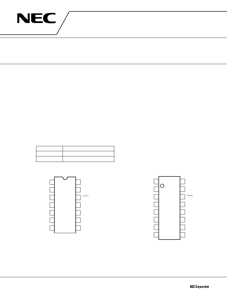
ORDERING INFORMATION
PART No.
PACKAGE
µ
PD4990AC
14-pin plastic DIP (300 mil)
µ
PD4990AG
16-pin plastic SOP (300 mil)
CONNECTION DIAGRAM (Top View)
µ
PD4990A
Document No. IC-1755 (1st edition)
Date Published March 1997 P
Printed in Japan
SERIAL I/O CALENDAR & CLOCK
CMOS LSI
1
14
2
13
3
12
4
11
5
10
6
9
7
C
2
C
1
C
0
STB
CS
DATA IN
GND
(V
SS
)
V
DD
(+)
X
TAL
X
TAL
OUT ENBL
TP
DATA OUT
CLK
PD4990AC
µ
8
1
16
2
15
3
14
4
13
5
12
6
11
7
C
2
C
1
C
0
NC
STB
CS
DATA IN
V
DD
(+)
X
TAL
X
TAL
NC
OUT ENBL
TP
DATA OUT
PD4990AG
NC: NO CONNECTION
µ
10
8
9
GND
(V
SS
)
CLK

µ
PD4990A
2
ABSOLUTE MAXIMUM RATINGS
Supply Voltage
V
DD
-
V
SS
-
0.5 to 7.0
V
Input Voltage
V
IN
V
SS
-
0.3 to V
DD
+0.3
V
Operating Temperature Range
T
opt
-
40 to +85
∞
C
Storage Temperature Range
T
stg
-
65 to +125
∞
C
Output Terminal Voltage
V
OUT
-
0.5 to 7.0
V
ELECTRICAL CHARACTERISTICS (f = 32.768 kHz, C
G
= C
D
= 20 pF, C
I
= 20 k
, T
a
= 25
∞
C)
CHARACTERISTIC
SYMBOL
MIN.
TYP.
MAX.
UNIT
TEST CONDITIONS
Operating Voltage
V
DD
-
V
SS
2.00
5.50
V
8
20
µ
A
V
DD
-
V
SS
= 3.60 V
Current Consumption
I
DD
100
µ
A
V
DD
-
V
SS
= 5.50 V
V
DD
-
V
SS
= 2.0 to 5.5 V
Low Level Output Voltage
V
OL
0.4*
V
I
OL
= 500
µ
A
CLK Input Frequency
f
CLK
DC
500
kHz
V
DD
-
V
SS
= 2.0 V, Duty 50 %
Input Leakage Current
I
IN
±
1
µ
A
V
DD
-
V
SS
= 5.50 V
High Level Input Voltage
V
IH
0.7 V
DD
V
DD
V
Low Level Input Voltage
V
IL
V
SS
0.3 V
DD
V
* TP and DATA OUT are N-channel open drain output.
A.C. ELECTRICAL CHARACTERISTICS (f = 32.768 kHz, V
DD
-
V
SS
= 2.0 V, T
a
= 25
∞
C)
CHARACTERISTIC
SYMBOL
MIN.
TYP.
MAX.
UNIT
TEST CONDITIONS
C
0 to 2
, CS
-
STB Set-up Time
t
SU
1
µ
s
STB Pulse Width
t
STB
1
µ
s
C
0 to 2
, CS
-
STB Hold Time
t
HLD
1
µ
s
STB LATCH Delay Time
t
d1
1**
µ
s
except Time Read mode
CLK-DATA OUT Delay time
t
d(c-o)
1
µ
s
R
L
= 33 k
, C
L
= 15 pF
DATA IN Set-up Time
t
DSU
1
µ
s
DATA IN Hold Time
t
DHLD
1
µ
s
** Note: When a function mode is Time Read mode (other than Test mode), STB LATCH delay time is 20
µ
s MAX.
(t
d2
).

3
µ
PD4990A
BLOCK DIAGRAM
DATA
OUT
TP
MPX
MPX
SEC
D/W
MON -TH
HOUR
MIN
YEAR
DAY
SEC
1/2
15
1/2
6
C
3
'
C
3
' C
2
' C
1
' C
0
'
C
2
'
C
1
'
C
0
'
C
2
OE
CLK
CLK
CLK RH
DATA
IN
CS
STB
C
1
C
0
X
TAL
X
TAL
1 Hz
64 Hz
1 Hz
TEST
PS
OSC
CS
COMMAND
Register
DECODER
DATA SELECTOR
Select signal
generator circuit
Time counter
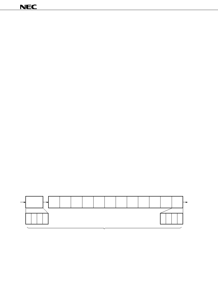
48 Bit Shift Register
STOP
RESET
15 Stage Binary Divider
N-ch
OPEN DRAIN
MPX
PS
D/W
CS
TP
RH
:
:
:
:
:
:
Multiplexer
Preset
Day of the Week
Chip Select
Timing Pulse
Register Hold
µ
PD4990A
4
FUNCTION SPECIFICATIONS
∑
Crystal frequency (X tal osc.).
∞
32.768 kHz
∑
Data
Data types are: second, minute, day, week, month, and year.
Leap years, 31-day months, and months with 30 or less days are adjusted automatically.
A 24-hour system is used and last two digits of Gregorian year are indicated.
It is assumed that leap years are expressed by multiples of 4.
∑
Data format
Data is represented in BCD notation. Only months are represented in hexadecimal notation.
∑
Data input-output and Clock
Data is input/output synchronously with reference to the external clocks input from the CLK pin using the serial
input/output system. (See Fig. 1.)
∑
Timing pulse output
Three frequencies, 64 Hz, 256 Hz, and 2 048 Hz, can be set with C
0
, C
1
and C
2
pins.
Using serial data input command, selective timing pulses (TPs) are 64 Hz, 256 Hz, 2 048 Hz, and 4 096 Hz
and selective output intervals are 1, 10, 30, and 60 seconds.
∑
Function mode selection
A function mode can be selected by the inputs from C
0
, C
1
, and C
2
. Also a function mode can be selected through
serial data input. (C
0
= C
1
= C
2
= V
DD
)
Each command is latched with STB (strobe).
∑
Chip select
Connecting the CS pin to the ground level inhibits CLK and STB inputs.
∑
Data output inhibition
Connecting the OUT ENBL pin to the ground level sets the DATA OUT pin at high impedance.
Figure 1.
command
register
Ten's of
year
C
3
'
Unit of
year
month
52 Bit Shift Register
* DATA of 52 Bit Shift Register appears on DATA OUT terminal from LSB of second.
day of
the week
Ten's of
days
Unit of
days
Ten's of
hours
Unit of
hours
Ten's of
minutes
Unit of
minutes
Ten's of
seconds
LSB
MSB
Unit of
seconds
C
2
' C
1
' C
0
'
D
3
D
2
D
1
D
0

5
µ
PD4990A
TERMINALS
∑
Input terminals
∞
DATA IN
Data input of 40-/52-bit shift register
∞
CLK
Shift clock input of 40-/52-bit shift register
∞
C
0
, C
1
, C
2
Command input (3 bit)
∞
STB
Strobe input
∞
CS
Chip select input (Prohibits CLK & STB)
∞
OUT ENBL
Output control input (Makes the DATA OUT high impedance by inputting low level).
∑
Output terminals (N-channel Open Drain)
∞
DATA OUT
Data output of 40-/52-bit shift register
∞
TP
Timing pulse output
∑
Oscillation terminals
∞
X
TAL
Oscillation inverter input (OSC IN)
∞
X
TAL
Oscillation inverter output (OSC OUT)
∑
Power supply terminals
∞
V
DD
Plus power supply
∞
GND (V
SS
)
Common line