Document Outline
- COVER
- DESCRIPTION
- FEATURES
- ORDERING INFORMATION
- PIN CONFIGURATION (TOP VIEW)
- BLOCK DIAGRAM
- DIFFERENCES AMONG PRODUCTS
- 1. PROGRAM COUNTER (PC)
- 2. STACK POINTER (SP)
- 3. PROGRAM MEMORY (ROM)
- 4. DATA MEMORY (RAM)
- 5. DATA POINTER (R0 )
- 6. ACCUMULATOR (A)
- 7. ARITHMETIC LOGIC UNIT (ALU)
- 8. FLAGS
- 9. SYSTEM CLOCK GENERATOR
- 10. TIMER
- 11. PIN FUNCTIONS
- 11.1 KI/O PIN (P0)
- 11.2 KI/O PULL-DOWN RESISTOR CONFIGURATION
- 11.3 KI PIN (P12)
- 11.4 KI PULL-DOWN RESISTOR CONFIGURATION
- 11.5 S-OUT PIN
- 11.6 S-IN PIN (D0 BIT OF P1)
- 12. PORT REGISTER (Px)
- 13. CONTROL REGISTER (P1)
- 14. STANDBY FUNCTION (HALT INSTRUCTION)
- 14.1 STOP MODE (OSCILLATION STOP HALT INSTRUCTION)
- 14.2 HALT MODE (OSCILLATION CONTINUE HALT INSTRUCTION)
- 14.3 STANDBY RELEASE CONDITIONS
- 15. AC PIN (ALL CLEAR PIN)
- 16. LOW-VOLTAGE DETECTOR (RESET) CIRCUIT
- 17. MASK OPTIONS (PLA DATA)
- 18. PROGRAM DEVELOPMENT TOOLS
- 19. ORDERING ROM CODE
- 20. INSTRUCTION SET
- 21. APPLICATION CIRCUIT EXAMPLE
- 22. ELECTRICAL SPECIFICATIONS
- (1) uPD6124A Electrical Specifications
- (2) uPD6600A Electrical Specifications
- 23. CHARACTERISTICS CURVE (REFERENCE VALUE) (Common in uPD6124A and 6600A)
- 24. PACKAGE DRAWINGS
- 25. RECOMMENDED SOLDERING CONDITIONS
- APPENDIX uPD612 x SERIES PRODUCT LIST

©
1989
DATA SHEET
MOS INTEGRATED CIRCUIT
µ
PD6124A, 6600A
DESCRIPTION
The
µ
PD6124A and 6600A are 4-bit single-chip microcontrollers for infrared remote controllers for TVs, VCRs,
stereos, cassette decks, air conditions, etc.
These microcontrollers consist of ROM, RAM, a 4-bit parallel-processing ALU, a programmable timer, key input/
output ports, and transmit output ports. Functioning is controlled by a program.
A one-time PROM, model
µ
PD61P24, to which a program can be written only once is also available. This one-time
PROM is ideal for evaluation of programs running in a
µ
PD6124A or 6600A, and for small-scale production of such
systems.
FEATURES
∑
Transmitter for programmable infrared remote control-
ler
∑
19 types of instructions
∑
Instruction execution time: 17.6
µ
s (with 455-kHz ce-
ramic resonator)
∑
Program memory (ROM) capacity
∑
µ
PD6124A: 1002
◊
10 bits
∑
µ
PD6600A: 512
◊
10 bits
∑
Data memory (RAM) capacity: 32
◊
5 bits
∑
9-bit programmable timer: 1 channel
∑
I/O pins (K
I/O
): 8 pins
∑
Input pins (K
I
): 4 pins
∑
Serial input pins (S-IN): 1 pin
∑
Transmission-in-progress indication pin (S-OUT): 1
pin
∑
Transmit carrier frequency (REM)
f
OSC
/12, f
OSC
/8
∑
Standby operation (HALT/STOP mode)
∑
Low power consumption
∑
Current consumption in STOP mode (T
A
= 25
∞
C)
∑
Low-voltage operation
µ
PD6124A: V
DD
= 2.2 to 5.5 V
µ
PD6600A: V
DD
= 2.2 to 3.6 V
Caution
To use the NEC transmission format, ask NEC to supply the custom code.
Do not use R
0
when using a register as an operand of the branch instruction.
4-BIT SINGLE-CHIP MICROCONTROLLER
FOR REMOTE CONTROL TRANSMISSION
Document No. U12391EJ5V0DS00 (5th edition)
(Previous No. IC-1927)
Date Published June 1997 N
Printed in Japan
The information in this document is subject to change without notice.
The mark
shows major revised points.

µ
PD6124A, 6600A
2
ORDERING INFORMATION
Part Number
Package
µ
PD6124ACS-XXX
20-pin plastic shrink DIP (300 mil)
µ
PD6124AGS-XXX
20-pin plastic SOP (300 mil)
µ
PD6600ACS-XXX
20-pin plastic shrink DIP (300 mil)
µ
PD6600AGS-XXX
20-pin plastic SOP (300 mil)
Remark
XXX indicates ROM code suffix.
PIN CONFIGURATION (TOP VIEW)
K
K
S-IN
S-OUT
REM
V
OSC-OUT
OSC-IN
V
AC
1
2
3
4
5
6
7
8
9
10
20
19
18
17
16
15
14
13
12
11
K
K
K
K
K
K
K
K
K
K
I/O2
I/O3
I/O4
I/O5
I/O6
I/O7
I0
I1
I2
I3
I/O1
I/O0
DD
SS

µ
PD6124A, 6600A
3
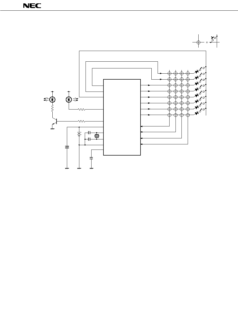
BLOCK DIAGRAM
I0 I3
K -K
L
H
32 5 bits
◊
AC
K
I/O0
-K
I/O7
S-IN
REM
S-OUT
OSC-IN
OSC-OUT
MOD
10 bits
OSC
To S-OUT
ROM
D.P.
ROM
D.P.
PC(H)
M
P
X
Note
ADD
DEC
M
P
X
RAM
RAM
CNTL
(H)
CNTL
(L)
SP
TIMER
(L)
TIMER
(H)
ACC
KEY
IN
KEY
OUT(H)
KEY
OUT(L)
ALU
Watchdog
timer
function
Low-
voltage
detector
circuit
PC(L)
ROM
(L)
ROM
(H)
Note ROM capacity depends on the products.
DIFFERENCES AMONG PRODUCTS
Item
Product Name
µ
PD6124A
µ
PD6600A
ROM Capacity
1002
◊
10 bits (Mark ROM)
512
◊
10 bits (Mask ROM)
RAM Capacity
32
◊
5 bits
I/O Pins
8 (K
I/O0
-
KI/O7
)
S-IN Pins
Provided
Current Consumption
2
µ
A
(f
OSC
= STOP) (MAX.)
S-IN High Level Input
30
µ
A
Current (MAX.)
Transmit Carrier Frequency
f
OSC
/12, f
OSC
/8
Low-voltage Detector
Provided
(Reset) Circuit
Supply Current
V
DD
= 2.2 to 5.5 V
V
DD
= 2.2 to 3.6 V
Package
∑ 20-pin plastic SOP (300 mil)
∑ 20-pin plastic shrink DIP (300 mil)

µ
PD6124A, 6600A
4
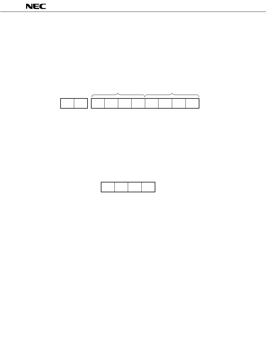
1.
PROGRAM COUNTER (PC) ......... 9 BITS
:
µ
PD6600A
10 BITS
:
µ
PD6124A
The program counter (PC) is a binary counter, which holds the address information for the program memory.
Figure 1-1. Program Counter Organization
PC
7
PC
6
PC
5
PC
4
PC
3
PC
2
PC
1
PC
0
PC
8
PC
9
PC
7
PC
6
PC
5
PC
4
PC
3
PC
2
PC
1
PC
0
PC
8
PC
PC
PD6124A
(b)
PD6600A
(a)
µ
µ
Normally, the program counter contents are automatically incremented each time an instruction is executed,
according to the number of instruction bytes.
When executing a jump instruction (JMP0, JC, JF), the program counter indicates the jump destination.
Immediate data or the data memory contents are loaded to all or some bits of the PC.
When executing the call instruction (CALL0), the PC contents are incremented (+1) and saved into the stack memory.
Then, a value needed for each jump instruction will be loaded.
When executing the return instruction (RET), the stack memory contents are double incremented (+2) and loaded
into the PC.
When "all clear" is input or on reset, the PC contents are cleared to "000H".
2.
STACK POINTER (SP) ......... 2 BITS
This 2-bit register holds the start address information for the stack area. The stack area is shared with the data
memory.
The SP contents are incremented, when the call instruction (CALL0) is executed. They are decremented, when the
return instruction (RET) is executed.
The stack pointer is cleared to "00B" after reset or "all clear" is input, and indicates the highest address FH for the
data memory as the stack area.
The figure below shows the relationship for the stack pointer and the data memory area.
R
C
Data memory
R
D
R
E
R
F
(SP)
11B
10B
01B
00B
If the stack pointer overflows or underflows, it is determined that the CPU overflows, and the PC internal reset signal
will be generated.

µ
PD6124A, 6600A
5
3.
PROGRAM MEMORY (ROM) ......... 512 STEPS
◊
10 BITS
:
µ
PD6600A
1002 STEPS
◊
10 BITS :
µ
PD6124A
The program memory (ROM) is configured in 10 bits steps. It is addressed by the program counter.
Program and table data are stored in the program memory.
Figure 3-1. Program Memory Map
000H
0FFH
100H
1FFH
Test program
area
PD6124A
(b)
PD6600A
(a)
000H
0FFH
100H
1FFH
200H
2FFH
300H
3E9H
3EAH
3FFH
µ
µ
4.
DATA MEMORY (RAM) ......... 32 WORDS
◊
5 BITS
The data memory is a RAM of 32 words
◊
5 bits. The data memory stores processing data. In some cases, the
data memory is processed in 8-bit units. R
0
may be used as the data pointer for the ROM.
After power application, the RAM will be undefined. The RAM retains the previous data on reset.
Figure 4-1. Data Memory Organization
1
R
0
0
R
F
R
B
R
C
SP≠3
SP≠2
SP≠1
SP≠0
.
.
.
.
.
.
Caution
Avoid using the RAM areas R
D
, R
E
, and R
F
in a CALL routine as much as possible because these areas
are also used as stack memory areas (to prevent program hang-up in case the value of the SP is
destroyed due to some reason such as noise).
When using these RAM areas as general-purpose RAM areas, be sure to include stack pointer
checking in the main routine.
0
0
1
1
0
0
1
1
µ
PD6124A, 6600A
6
5.
DATA POINTER (R
0
)
R
0
(R
10
, R
00
) for the data memory can serve as the data pointer for the ROM.
R
0
specifies the low-order 8 bits in the ROM address. The high-order 2 bits in the ROM address are specified by
the control register.
Table referencing for ROM data can be easily executed by calling the ROM contents by setting the ROM address
to the data pointer.
On reset or "all clear" is input, it becomes undefined.
Figure 5-1. Data Pointer Organization
AD
0
AD
1
AD
2
AD
3
AD
4
AD
5
AD
6
AD
7
AD
8
AD
9
Note
Control registers
(P )
1
R
0
R
10
R
00
Note
µ
PD6600A: AD
9
= 0
6.
ACCUMULATOR (A) ......... 4 BITS
The accumulator (A) is a 4-bit register. The accumulator plays a major role in each operation.
On reset or "all clear" is input, it becomes undefined.
Figure 6-1. Accumulator Organization
A
0
A
1
A
2
A
3
A
7.
ARITHMETIC LOGIC UNIT (ALU) ......... 4 BITS
The arithmetic logic unit (ALU) is a 4-bit operation circuit, and executes simple operations, such as arithmetic
operations.
8.
FLAGS
(1)
Status flag
When the status for each pin is checked by the STTS instruction, if the condition coincides with the condition
specified by the STTS instruction, the status flag (F) is set (to 1).
On reset or "all clear" is input, it becomes undefined.
(2)
Carry flag
When the INC (increment) instruction or the RL (rotate left) instruction is executed, if a carry is generated from
the MSB for the accumulator, the carry flag (C) is set (to 1).
The carry flag (C) is also set (to 1), if the contents for the accumulator are "FH", when the SCAF instruction
is executed.
On reset or "all clear" is input, it becomes undefined.

µ
PD6124A, 6600A
7
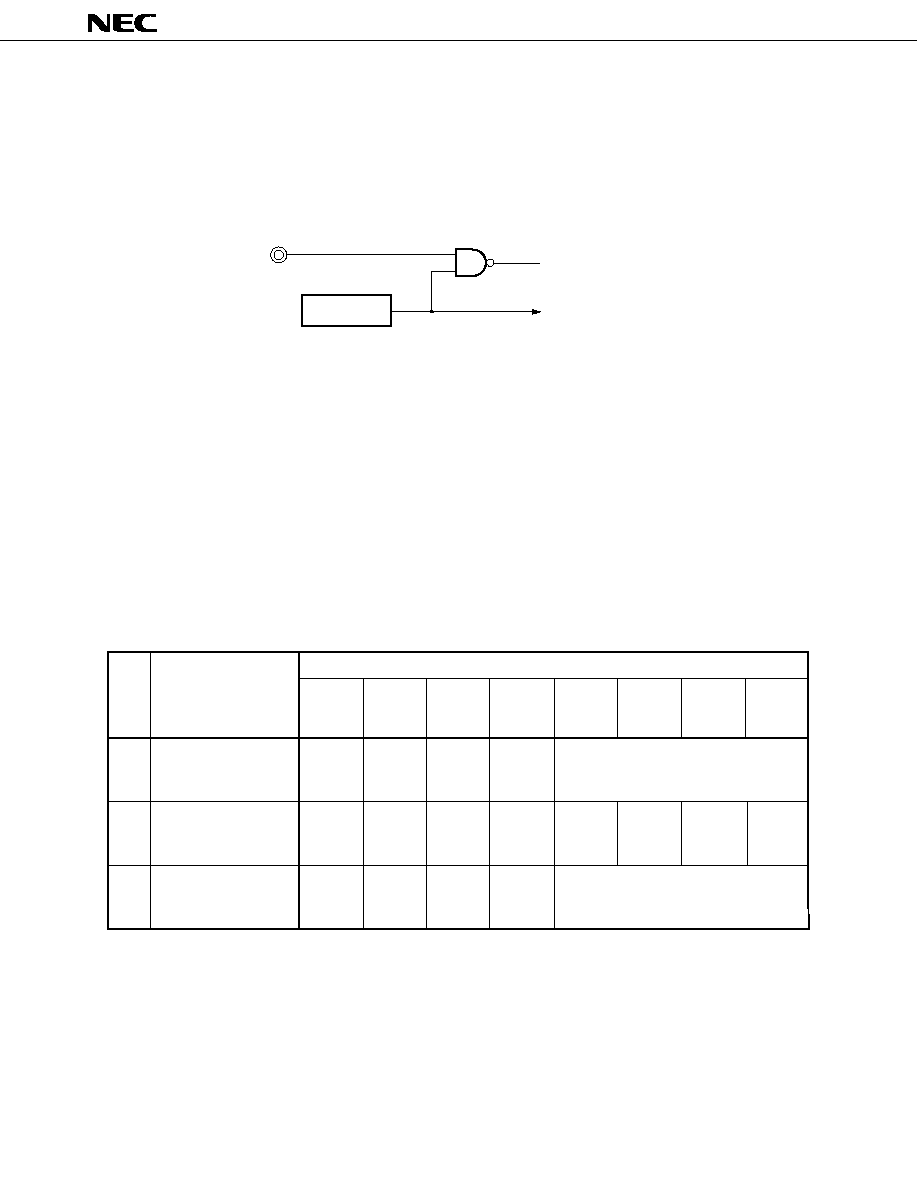
9.
SYSTEM CLOCK GENERATOR
The system clock generator consists of a resonator, which uses a ceramic resonator (400kHz to 500kHz).
Figure 9-1. System Clock Generator
STOP mode
System clock
¯
OSC-OUT
OSC-IN
In the STOP mode (oscillation stop HALT instruction), the oscillator in the system clock generator stops its operation,
and the system clock ¯ is stopped.

µ
PD6124A, 6600A
8
10. TIMER
The timer block determines the transmission output pattern. The timer consists of 10 bits, of which 9 bits serve as
the 9-bit down counter and the remaining 1 bit serves as the 1-bit latch, which determines the carrier output validity.
The 9-bit down counter is decremented (≠1) every 8/f
OSC
(s) in synchronization with the machine cycle, after starting
down count operation. Down counting stops after all of the 9 bits become 0. When down counting is stopped, the signal
indicating that the timer operation has stopped, is output. If the CPU is at standby (HALT TIMER) for the timer operation
completion, the standby (HALT) condition is released and the next instruction will be executed. If the next instruction
again sets the value of the down counter, down counting continues without any error (the carrier output of the REM pin
is not affected).
Set the down count time according to the following calculation; (set value (HEX) + 1)
◊
8/f
OSC
. Setting the value to
the timer is done by the timer manipulation instruction.
When the down counter is operating, the remote control transmission carrier can be output to the REM pin. Whether
or not to output the carrier can be selected by the MSB for the timer register block. Set "1", when outputting the carrier,
or "0", when not outputting the carrier.
If all the down counter bits become "0", when outputting the carrier, the carrier output will be stopped. When not
outputting the carrier, the REM pin output will become low level.
A signal in synchronization with the REM output is output to the S-OUT pin. However, the waveform for the S-OUT
pin is low, when the carrier is being output to the REM pin, or it is high, when the carrier is not being output to the REM
pin.
If the HALT instruction, which initiates the oscillation stop mode, is executed when the down counter is operating,
the oscillation stop mode is initiated after down counting is stopped (after 0).
Timer operation STOP/RUN is controlled by the control register (P
1
). (Refer to 13. CONTROL REGISTER (P
1
).)
At reset (all clear) time, the REM pin goes low and S-OUT pin goes high. All 10 bits of the timer are cleared to 000H.
Cautions 1. Because the timer clock is not synchronized with the carrier output, the pulse width may be
shortened at the beginning and end of the carrier output.
2. Reset caused by the low-voltage detector circuit causes the S-OUT pin to output low level.
Figure 10-1. Timer Block Organization
From low-voltage
detector (reset)
circuit
S-OUT
REM
Carrier
(fosc/12, fosc/8)
Selected by control register
Clear
Set by timer mainpulation instruction
9-bit down counter
Zero detection circuit
D of control register P
(Timer RUN/STOP)
2
1
1/0
MSB
fosc/8

µ
PD6124A, 6600A
9
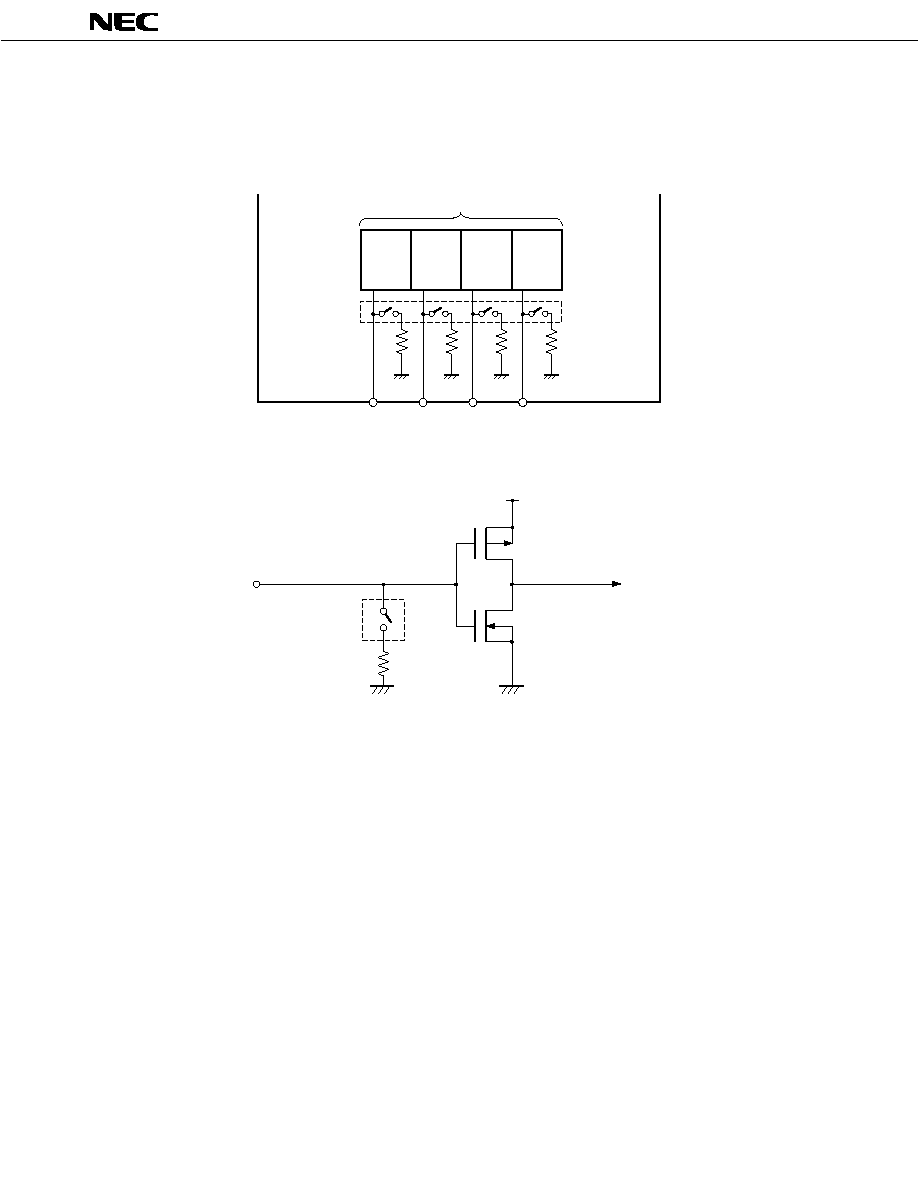
11. PIN FUNCTIONS
11.1
K
I/O
PIN (P
0
)
This is the 8-bit I/O pin for key-scan output. When the control register (P
1
) is set for the input port, the port can be
used as an 8-bit input pin. When the port is set for the input mode, all of these pins are pulled down to the V
SS
level
inside the LSI.
At reset (all cleared), the value of I/O mode and output latch becomes undefined.
Figure 11-1. K
I/O
Pin Organization
K
I/O7
K
I/O6
K
I/O5
K
I/O4
K
I/O3
K
I/O2
K
I/O1
K
I/O0
P
0
P
10
P
00
(P )
Control register
1
11.2
K
I/O
PULL-DOWN RESISTOR CONFIGURATION
V
DD
V
SS
CMOS
N-ch
Pin
Pull-down resistor
Input signal
Output signal
Input/output selection
N-ch
P-ch
R
When K
I/O
is set to the input mode, pull-down resistor R is turned on.
µ
PD6124A, 6600A
10
11.3
K
I
PIN (P
12
)
This is the 4-bit pin for key input. All of these pins can be pulled down to the V
SS
level by mask option.
Figure 11-2. K
I
Pin Organization
P
12
K
I3
K
I2
K
I1
K
I0
P
2
Mask option
11.4
K
I
PULL-DOWN RESISTOR CONFIGURATION
V
DD
V
SS
N-ch
V
SS
Pin
Input signal
K pull-down
resistor switch
(Mask option)
Pull-down
resistor
I
P-ch
When the pull-down resistor switch is turned on (set 1) by the mask option, pull-down resistor R is turned on.
Caution
When using the pin as the key switch, turn on the pull-down resistor switch by the mask option.

µ
PD6124A, 6600A
11
11.5
S-OUT PIN
By going low whenever the carrier frequency is output from the REM pin, the S-OUT pin indicates that communication
is in progress.
The S-OUT pin is CMOS output.
The S-OUT pin goes high on reset.
11.6
S-IN PIN (D
0
BIT OF P
1
)
To input serial data, use the S-IN pin. When control register (P
1
) is set to serial input mode, the S-IN pin is connected
as an input to the LSB of the accumulator; the S-IN pin can be pulled down to the V
SS
level by a mask option from within
the LSI. In this state, if the rotate-left accumulator instruction (RL A) is executed, the data on the S-IN pin is copied
to the LSB of the accumulator.
If the control register is released from serial input mode, the S-IN pin goes into a high-impedance state, but no through
current flows internally.
When the RL A instruction is executed, the MSB is copied to the LSB.
At reset (all cleared), the S-IN pin goes into a high-impedance state.
Caution
The
µ
PD6123 is not provided with an S-IN pin.
Figure 11-3. Configuration of the S-IN Pin
A
3
A
2
A
1
A
0
CY
Control register
S-IN
Mask option
µ
PD6124A, 6600A
12
12. PORT REGISTER (P
◊
)
K
I/O
, K
I
, and the control register are handled as port registers.
The table below shows the relations between the port registers and pins.
Table 12-1. Relations between Port Registers and Pins
Pin
Input Mode
Output Mode
Name
Read
Write
Read
Write
On Reset
K
I/O
Pin status
Output latch
Pin status
Output latch
Undefined [input mode, output latch]
K
I
Pin status
≠
≠
≠
Input mode
S-IN
Pin status is read by RL A instruction when D
0
of P
1
register = 1.
High impedance (D
0
of P
1
register = 0)
P
10
P
11
P
12
P
00
P
01
P
02
K
I/O7-4
K
I/O3-0
P
0
P
1
P
2
Control register (H)
Control register (L)
K
I3-0
P
1
◊
(H)
P
0
◊
(L)
µ
PD6124A, 6600A
13
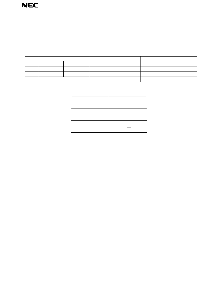
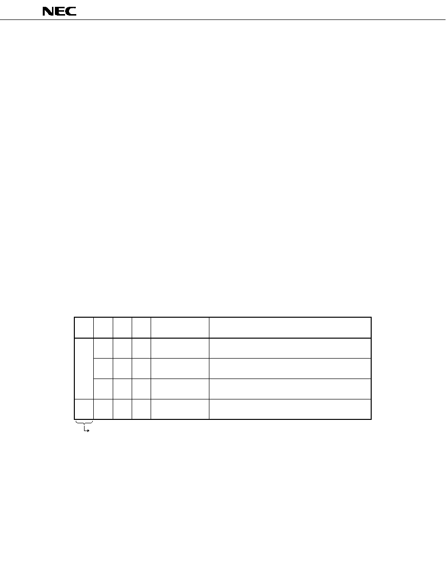
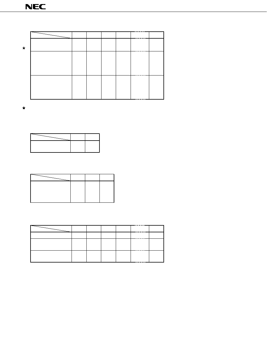
13. CONTROL REGISTER (P
1
)
The control register contains of 10 bits. The controllable items are shown in Table 13-1.
Table 13-1. Control Register (P
1
) (1/2)
(a)
µ
PD6124A
Bit
D
9
Name
Test mode
≠
Be sure to set 0.
0
1
Set
Value
Timer
D
8
D
7
D
6
D
5
D
4
D
3
D
2
D
1
D
0
HALT
D.P.
AD
MOD
K
I/O
9
D.P.
AD
8
RL A
A
CC
0
STOP
NOP
f /8
AD =0
9
AD =0
8
OSC
IN
RUN
OSC
STOP
f /12
AD =1
9
AD =1
8
OSC
OUT
A
3
S-IN
D
0 ..........................
Specifies data to be input to A
0
when the accumulator is shifted to the left.
0: A
3
, 1:S-IN
D
1 ..........................
Specifies the status of K
I/O
, as follows:
0: input mode, 1: output mode
D
2 ..........................
Specifies the status of the timer, as follows:
0: Count stop, 1: Count execution
D
3 ..........................
Specifies the carrier frequency output from the REM pin.
0: f
OSC
/8, 1: f
OSC
/12
D
4
, D
5 .................
Specify the high-order 2 bits of the ROM data pointer.
D
6 ..........................
Determines what happen to the oscillation circuit when the HALT instruction is executed.
0: Oscillation does not stop
1: Oscillation stops (STOP mode)
D
7 ..........................
Be sure to set this bit to 0.
D
8
, D
9 .................
These bits specify test modes. Be sure to set them to 0.
Remark
D
0
= D
8
= D
9
= 0 on reset, and the other bits are undefined.

µ
PD6124A, 6600A
14
Table 13-1. Control Register (P
1
) (2/2)
(b)
µ
PD6600A
Bit
D
9
Name
Test mode
≠
Be sure to set 0.
0
1
Set
Value
Timer
D
8
D
7
D
6
D
5
D
4
D
3
D
2
D
1
D
0
HALT
D.P.
AD
MOD
K
I/O
9
D.P.
AD
8
RL A
A
CC
0
STOP
NOP
f /8
AD =0
8
OSC
IN
RUN
OSC
STOP
f /12
AD =1
8
OSC
OUT
A
3
S-IN
Be sure to
set 0.
D
0 ..........................
Specifies data to be input to A
0
when the accumulator is shifted to the left.
0: A
3
, 1:S-IN
D
1 ..........................
Specifies the status of K
I/O
, as follows:
0: input mode, 1: output mode
D
2 ..........................
Specifies the status of the timer, as follows:
0: Count stop, 1: Count execution
D
3 ..........................
Specifies the carrier frequency output from the REM pin.
0: f
OSC
/8, 1: f
OSC
/12
D
4 ..........................
Specify the MSB of the ROM data pointer.
D
5 ..........................
Be sure to reset them to 0.
D
6 ..........................
Determines what happen to the oscillation circuit when the HALT instruction is executed.
0: Oscillation does not stop
1: Oscillation stops (STOP mode)
D
7 ..........................
Be sure to set this bit to 0.
D
8
, D
9 .................
These bits specify test modes. Be sure to set them to 0.
Remark
D
0
= D
8
= D
9
= 0 on reset, and the other bits are undefined.
µ
PD6124A, 6600A
15
14. STANDBY FUNCTION (HALT INSTRUCTION)
The
µ
PD6600A is provided with the standby mode (HALT instruction), in order to reduce the power consumption,
when not executing the program. Clock oscillation can be stopped in the standby mode (STOP mode).
In the standby mode, the program execution stops. However, the contents of the internal registers and the data
memory are all retained.
14.1
STOP MODE (OSCILLATION STOP HALT INSTRUCTION)
In the STOP mode, the operation of the system clock generator (ceramic resonator oscillation circuit) stops.
Therefore, operations requiring the system clock will stop.
If the HALT instruction is executed during timer operation, the program counter stops. The oscillation stop mode
will be initiated, after the timer count down operation is completed.
14.2
HALT MODE (OSCILLATION CONTINUE HALT INSTRUCTION)
The CPU stops its operation, until the HALT release condition is satisfied.
The system clock operation continues in this mode.
14.3
STANDBY RELEASE CONDITIONS
(1)
S-IN input
(2)
K
I/O
input
(3)
K
I
input
(4)
Timer count down operation completion
Remark
Either high level or low level can be specified for setting a release condition by input.
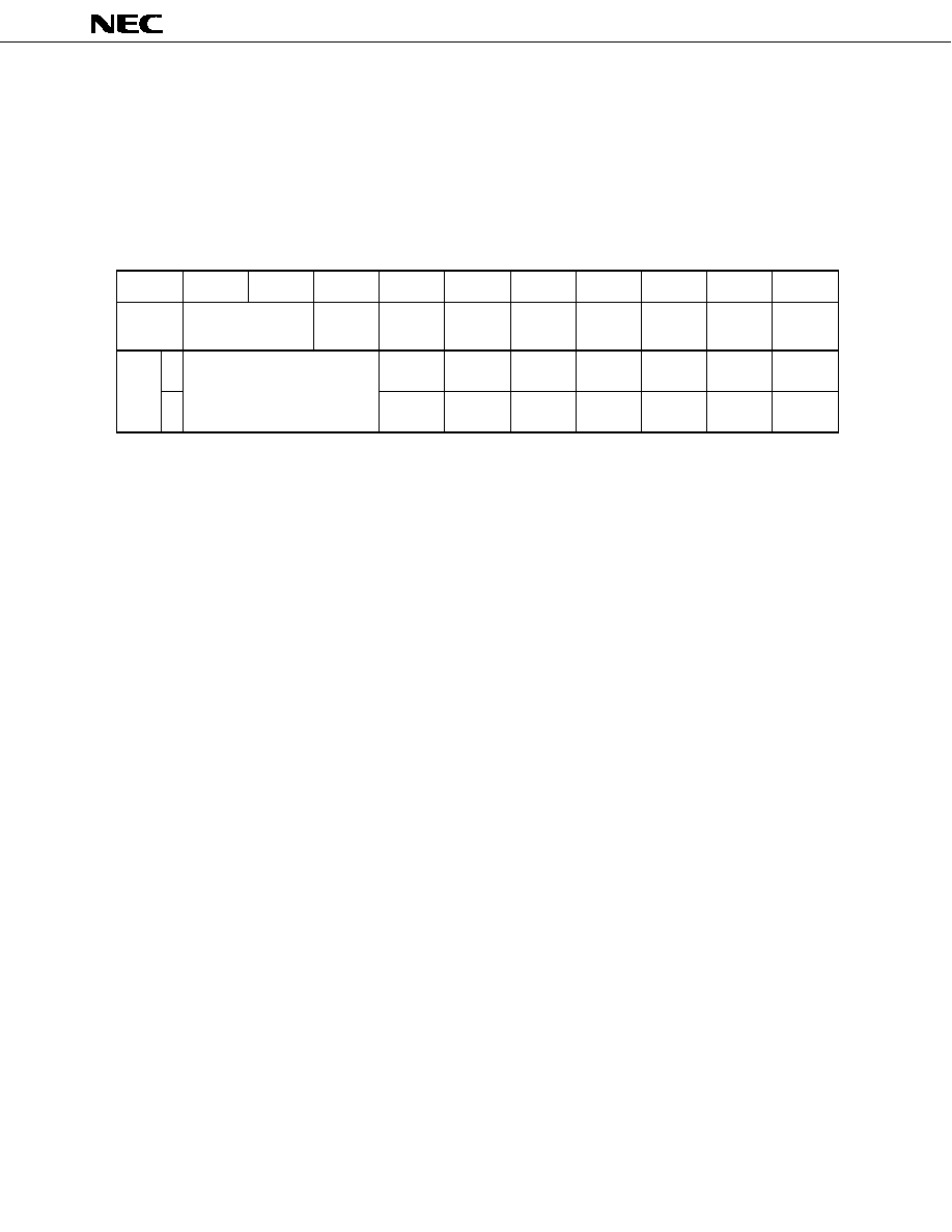
Table 14-1. Standby Mode Releasing Condition
D
3
0/1
0
Releasing condition:
0
1
Timer
0
1
0
0
K
0
0
S-IN
D
2
D
1
D
0
Releasing
Condition
1
0
1
0
I/O
K
I
Remarks
Released when 0.
Valid only in the IN mode.
When RL A is selected, the standby mode is
always released.
3
"0"∑∑∑Low level detection
"1"∑∑∑High level detection

µ
PD6124A, 6600A
16
15. AC PIN (ALL CLEAR PIN)
Internal part of the CPU including the program counter can be reset by setting the AC pin to the low level.
WATCHDOG TIMER FUNCTION
A power-on reset function and a CR watchdog timer function, that can be controlled by program, can be realized
by connecting a 0.1
µ
F capacitor across the AC pin and the V
SS
.
V
DD
0.1 F
µ
0.1 F
µ
V
V
DD
V
thL
t
Charge mode
Charge start instruction
Execute HALT instruction
immediately before NOP.
(Charge for 0.4 ms or more)
Discharge mode
Charge-discharge
pattern
Discharge start instruction
Discharge starts after the NOP
instruction execution.
(Discharge time is about 5 ms from V
DD
to V
thL
)
The pattern must be
controlled by the program,
in such a manner that
the C charge level will not
go below V
thL
.
Caution
When the watchdog timer function is not used, switch to charging mode by executing a NOP
instruction immediately before a HALT instruction at the beginning of the program. (Be sure to
connect the capacitor.)
µ
PD6124A, 6600A
17
16. LOW-VOLTAGE DETECTOR (RESET) CIRCUIT
The
µ
PD6124A and 6600A are internally provided with the low-voltage detector (reset) circuit, in order to prevent
program hang-up.
When V
DD
goes down to 1 V or below, an internal reset signal is generated. In the reset condition, a low level is
output to the S-OUT pin.
Reset circuit
Internal reset signal
AC pin
To S-OUT pin
Caution
The low-voltage detector circuit starts operating at a voltage ranging from 1 to 2.2 V. Hence, if the
supply voltage is 2 V or lower, the program counter may hang up before the low-voltage detector
circuit operates.
17. MASK OPTIONS (PLA DATA)
The following items can be selected by mask option selection:
∑ Provide/not provide K
I
, S-IN pin pull-down resistor
∑ Carrier duty selection (1/2, 1/3) at f
OSC
/12
∑ Hang-up detection specification
Mask option data should be registered at the object code end.
BIT ASSIGNMENT BY SWITCH SELECTION
0
1
2
7
K
0
K
ALL
6
K
0
HALT
S-IN
5
K
0
HALT
K
4
K
Duty
selection
HALT
K
Address
Note
I3
I2
I1
I0
I
I/O
I/O
3
0
2
0
1
S-IN
pull-down
resistor
0
0
MSB
LSB
K
I
pull-down resistor
Corresponding
Portion
Hang-up detection
Duty
S-IN
0
0
Note
The setting (bit) positions differ from the
µ
PD6125A and 6126A.
µ
PD6124A, 6600A
18
SWITCH FOR DATA
(1)
Pull-down resistor
When 0 ... Not provided (OFF)
When 1 ... Provided (ON)
(2)
Modulation duty (at f
OSC
/12)
When 0 ... 1/2 duty
When 1 ... 1/3 duty
(3)
Hang-up detection
<1> K
I/O
ALL
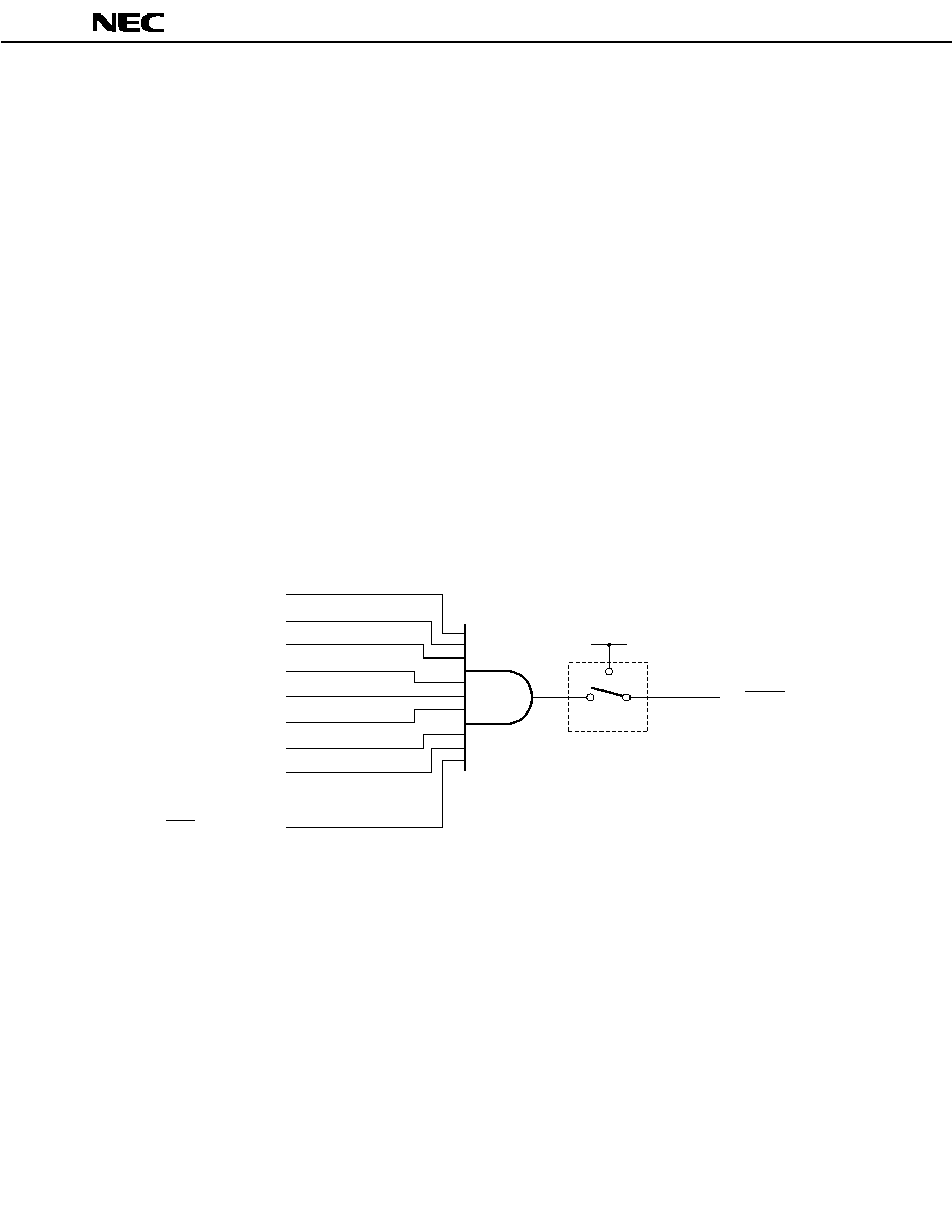
If the switch for hang-up detection K
I/O
ALL is set to ON (1) by mask option, the system is reset if, in oscillation
HALT (STOP) mode, the K
I/O
pin is in input mode, or if at least one of the K
I/O
pins is low (AC pin discharge
mode).
When 0 ... No reset function (OFF)
When 1 ... Reset function (ON)
Caution
To use a pin as a key source of a key matrix, be sure to set the switch to ON by mask option.
Figure 17-1. Hang-up Detection K
I/O
ALL Configuration Diagram
V
DD
To RESET circuit
Hang-up detection
K ALL switch
(Mask option)
K output signal
I/O0
K output signal
I/O1
K output signal
I/O2
K output signal
I/O3
K output signal
I/O4
K output signal
I/O5
K input/output selection
I/O
K output signal
I/O6
K output signal
I/O7
I/O
<2> HALT releasing condition specification (S-IN, K
I/O
, K
I
)
If the condition specified by mask option to be unused is satisfied in the HALT mode, the system is reset.
When 0 ... Used
When 1 ... Unused
Caution
Be sure to specify the HALT mode of the unused releasing condition to be unused (set).

µ
PD6124A, 6600A
19
18. PROGRAM DEVELOPMENT TOOLS
To develop programs for the
µ
PD6124A and 6600A, an assembler and an emulator for the
µ
PD612X series are
available from I.C. Corp. For details, contact IC Corp.
IC Corporation
6th Barnet Gotanda Bldg.
1-9-5 Higashi-Gotanda, Shinagawa-ku
Tel. 03-3447-3793
Fax. 03-3440-5606
Caution
To develop the programs for the
µ
PD6124A and 6600A, use the
µ
PD6124 because the
µ
PD6124A and
6600A are not available as the target devices for assembly and emulation.
The upper limit of ROM addresses is different in the
µ
PD6124A/6600A and
µ
PD6124. Make sure that
the program does not exceed 512 steps by checking the end address of the assembly listing after
assembling the program.
The mask option of the
µ
PD6124A/6600A is the same as that of the
µ
PD6124.
19. ORDERING ROM CODE
<1> To generate the data required for ordering a mask ROM, after assembling the program, convert the HEX file
to a ROM file by using the PROM utility program "UPDPROM".
Caution
When using "UPDPROM" select "27256" for PROM TYPE.
<2> Confirm that the instruction ROM code data is stored in addresses 0 through 7D3H (3FFH in
µ
PD6600A) of
the PROM.
Also confirm that the mask option ROM code data are stored in addresses 7FF0H through 7FF2H.

µ
PD6124A, 6600A
20
20. INSTRUCTION SET
ACCUMULATOR MANIPULATION INSTRUCTIONS
ANL
ANL
ANL
ANL
ORL
ORL
ORL
ORL
XRL
XRL
XRL
XRL
INC
RL
D00
E00
A00
D10
D30
D31
E10
E30
E31
A10
A30
A31
A13
F13
R
10
R
11
R
12
R
1F
R
00
R
01
R
0F
R
r
A, R
r
A, @R
0
H
A, @R
0
L
A, #data
A, R
r
A, @R
0
H
A, @R
0
L
A, #data
A, R
r
A, @R
0
H
A, @R
0
L
A, #data
A
A
D01
E01
A01
D02
E02
A02
D0F
E0F
A0F
D20
E20
A20
D21
E21
A21
D2F
E2F
A2F
≠
INPUT/OUTPUT INSTRUCTIONS
P
A,
P ,
A,
A,
A,
IN
OUT
ANL
ORL
XRL
F19
219
D19
E19
A19
P
P
11
P
P
P
A
P
P
P
P
P
P
P
F18
218
D18
E18
A18
P
10
F1A
21A
D1A
E1A
A1Z
P
12
F39
239
D39
E39
A39
P
01
F38
238
D38
E38
A38
P
00
F3A
23A
D3A
E3A
A3A
02
P
OUT
319
P
P
1
P
P
#data
318
P
0
31A
P
2
P
1P
and P
0P
operate in pair format
DATA TRANSFER INSTRUCTIONS
MOV
MOV
F00
F10
F01
F02
F0F
F20
F21
F2F
A, R
A, @R H
r
0
R
10
R
11
R
12
R
1F
R
00
R
01
R
0F
R
r
MOV
F30
A, @R H
0
MOV
F31
A, #data
MOV
MOV
300
301
302
30F
R , #data
R , @R
r
r
R
0
R
1
R
2
R
F
R
r
320
321
322
32F
MOV
R , A
r
200
201
202
20F
220
221
22F
0
R
1r
and R
0r
operate in pair format
µ
PD6124A, 6600A
21
BRANCH INSTRUCTIONS
R
r
R
0
R
1
R
2
R
F
≠
JMP0
JC
JC
JNC
JNC
JF
JF
JNF
JNF
addr
addr
Rr
Note
addr
addr
addr
411
611
≠
631
≠
711
≠
731
≠
Rr
Note
Rr
Note
Rr
Note
≠
≠
≠
≠
601
621
701
721
602
622
702
722
60F
62F
70F
72F
Pair register
JMP0
Rr
Note
≠
≠
401
402
40F
Note
r = 1 through F
r = 0 canot be used.
SUBROUTINE INSTRUCTIONS
addr
CALL0
RET
411
P
1
P
P
312
412
P
0
TIMER/COUNTER MANIPULATION INSTRUCTIONS
A,
T ,
T,
T,
MOV
MOV
MOV
MOV
F1F
21F
T
1
T
t
T
A
#data
@R
t
0
≠
31F
33F
T
0-1
T
0
t
F3F
23F
OTHER INSTRUCTIONS
HALT #data
STTS R
STTS #data
SCAF
NOP
00
R
111
131
D13
000
01
R
02
R
0F
R
120
121
122
12F
0r
µ
PD6124A, 6600A
22
21. APPLICATION CIRCUIT EXAMPLE
V
DD
V
DD
Key matrix
Mode select switch
Infrared LED
SE303 series
SE313
SE307-C
SE1003-C
Transmission
indication
2SC3616, 3618
2SD1615, 1616
2SC2001
3.0 V
47 F
µ
+
100 pF
100 pF
0.1 F
µ
K
I/O1
K
I/O0
S-IN
1
2
3
4
5
6
7
8
9
10
K
I/O2
K
I/O3
S-OUT
REM
V
DD
OSC-OUT
OSC-IN
V
SS
AC
K
I/O4
K
I/O5
K
I/O6
K
I/O7
K
I0
K
I1
K
I2
K
I3
PD6124A
PD6600A
µ
µ
20
19
18
17
16
15
14
13
12
11
Caution
The ceramic resonator start up capacitor value must be determined, by taking the voltage level and
the oscillation start up characteristics for the ceramic resonator into consideration.

µ
PD6124A, 6600A
23
22. ELECTRICAL SPECIFICATIONS
(1)
µ
PD6124A Electrical Specifications
ABSOLUTE MAXIMUM RATINGS (T
A
= 25
∞
C)
Parameter
Symbol
Ratings
Unit
Supply Voltage
V
DD
≠0.3 to +7.0
V
Input Voltage
V
IN
≠0.3 to V
DD
+ 0.3
V
Operating Ambient Temperature
T
A
≠20 to +75
∞
C
Storage Temperature
T
stg
≠40 to +125
∞
C
Caution
Even if one of the parameters exceeds its absolute maximum rating even momentarily, the quality
of the product may be degraded. The absolute maximum rating therefore specifies the upper or lower
limit of the value at which the product can be used without physical damages. Be sure to use the
product(s) within the ratings.
RECOMMENDED OPERATING RANGE (T
A
= ≠20 to +75
∞
C)
Parameter
Symbol
MIN.
TYP.
MAX.
Unit
Supply Voltage
V
DD
2.2
5.5
V
Oscillation Frequency
f
OSC
400
500
kHz
µ
PD6124A, 6600A
24
DC CHARACTERISTICS (V
DD
= 3.0 V, f
OSC
= 455 kHz, T
A
= 25
∞
C)
Parameter
Symbol
Conditions
MIN.
TYP.
MAX.
Unit
Supply Voltage
V
DD
2.2
5.5
V
Current Consumption 1
I
DD1
f
OSC
= 455 kHz
0.3
1.0
mA
Current Consumption 2
I
DD2
f
OSC
= STOP
2.0
µ
A
REM High Level Output Current
I
OH1
V
O
= 1.0 V
≠5
≠8
mA
REM Low Level Output Current
I
OL1
V
O
= 0.3 V
0.5
1.5
2.5
mA
S-OUT High Level Output Current
I
OH2
V
O
= 2.7 V
≠0.3
≠1.0
≠2.0
mA
S-OUT Low Level Output Current
I
OL2
V
O
= 0.3 V
1
1.5
mA
K
I
High Level Input Current
I
IH1
V
I
= 3.0 V
10
30
µ
A
K
I
High Level Input Current
I
IH1'
V
I
= 3.0 V, without pull-down resistor
0.2
µ
A
K
I
Low Level Input Current
I
IL1
V
I
= 0 V
≠0.2
µ
A
K
I/O
High Level Input Current
I
IH2
V
I
= 3.0 V
10
30
µ
A
K
I/O
High Level Input Current
I
IH2'
V
I
= 3.0 V, without pull-down resistor
0.2
µ
A
K
I/O
Low Level Input Current
I
IL2
V
I
= 0 V
≠0.2
µ
A
K
I/O
High Level Output Current
I
OH3
V
0
= 2.5 V
≠1.5
≠2.0
≠4.0
mA
K
I/O
Low Level Output Current
I
OL3
V
0
= 2.1 V
25
50
100
µ
A
S-IN High Level Input Current
I
IH3
V
I
= 3.0 V
6
30
µ
A
S-IN High Level Input Current
I
IH3'
V
I
= 3.0 V, without pull-down resistor
0.2
µ
A
S-IN Low Level Input Current
I
IL3
V
I
= 0 V
≠0.2
µ
A
K
I
High Level Input Voltage
V
IH1
2.1
3.0
V
K
I
Low Level Input Voltage
V
IL1
V
I
= 3.0 V
0
0.9
V
K
I/O
High Level Input Voltage
V
IH2
1.3
3.0
V
K
I/O
Low Level Input Voltage
V
IL2
0
0.4
V
S-IN High Level Input Voltage
I
IH3
1.1
3.0
V
S-IN Low Level Input Voltage
I
IL3
0
0.4
V
AC Pull-Up Resistor
R
1
V
I
= 0 V
0.3
3.0
k
AC Pull-Down Resistor
R
2
V
I
= 2.7 V
150
1500
k
AC High Level Input Voltage
V
IH4
1.8
3.0
V
AC Low Level Input Voltage
V
IL4
0
1.2
V

µ
PD6124A, 6600A
25
(2)
µ
PD6600A Electrical Specifications
ABSOLUTE MAXIMUM RATINGS (T
A
= 25
∞
C)
Parameter
Symbol
Ratings
Unit
Supply Voltage
V
DD
≠0.3 to +7.0
V
Input Voltage
V
IN
≠0.3 to V
DD
+ 0.3
V
Operating Ambient Temperature
T
A
≠20 to +75
∞
C
Storage Temperature
T
stg
≠40 to +125
∞
C
Caution
Even if one of the parameters exceeds its absolute maximum rating even momentarily, the quality
of the product may be degraded. The absolute maximum rating therefore specifies the upper or lower
limit of the value at which the product can be used without physical damages. Be sure to use the
product(s) within the ratings.
RECOMMENDED OPERATING RANGE (T
A
= ≠20 to +75
∞
C)
Parameter
Symbol
MIN.
TYP.
MAX.
Unit
Supply Voltage
V
DD
2.2
3.6
V
Oscillation Frequency
f
OSC
400
500
kHz
µ
PD6124A, 6600A
26
DC CHARACTERISTICS (V
DD
= 3.0 V, f
OSC
= 455 kHz, T
A
= 25
∞
C)
Parameter
Symbol
Conditions
MIN.
TYP.
MAX.
Unit
Supply Voltage
V
DD
2.2
3.6
V
Current Consumption 1
I
DD1
f
OSC
= 455 kHz
0.3
1.0
mA
Current Consumption 2
I
DD2
f
OSC
= STOP
2.0
µ
A
REM High Level Output Current
I
OH1
V
O
= 1.0 V
≠5
≠8
mA
REM Low Level Output Current
I
OL1
V
O
= 0.3 V
0.5
1.5
2.5
mA
S-OUT High Level Output Current
I
OH2
V
O
= 2.7 V
≠0.3
≠1.0
≠2.0
mA
S-OUT Low Level Output Current
I
OL2
V
O
= 0.3 V
1
1.5
mA
K
I
High Level Input Current
I
IH1
V
I
= 3.0 V
10
30
µ
A
K
I
High Level Input Current
I
IH1'
V
I
= 3.0 V, without pull-down resistor
0.2
µ
A
K
I
Low Level Input Current
I
IL1
V
I
= 0 V
≠0.2
µ
A
K
I/O
High Level Input Current
I
IH2
V
I
= 3.0 V
10
30
µ
A
K
I/O
High Level Input Current
I
IH2'
V
I
= 3.0 V, without pull-down resistor
0.2
µ
A
K
I/O
Low Level Input Current
I
IL2
V
I
= 0 V
≠0.2
µ
A
K
I/O
High Level Output Current
I
OH3
V
O
= 2.5 V
≠1.5
≠2.0
≠4.0
mA
K
I/O
Low Level Output Current
I
OL3
V
O
= 2.1 V
25
50
100
µ
A
S-IN High Level Input Current
I
IH3
V
I
= 3.0 V
6
30
µ
A
S-IN High Level Input Current
I
IH3'
V
I
= 3.0 V, without pull-down resistor
0.2
µ
A
S-IN Low Level Input Current
I
IL3
V
I
= 0 V
≠0.2
µ
A
K
I
High Level Input Voltage
V
IH1
2.1
3.0
V
K
I
Low Level Input Voltage
V
IL1
V
I
= 3.0 V
0
0.9
V
K
I/O
High Level Input Voltage
V
IH2
1.3
3.0
V
K
I/O
Low Level Input Voltage
V
IL2
0
0.4
V
S-IN High Level Input Voltage
I
IH3
1.1
3.0
V
S-IN Low Level Input Voltage
I
IL3
0
0.4
V
AC Pull-Up Resistor
R
1
V
I
= 0 V
0.3
3.0
k
AC Pull-Down Resistor
R
2
V
I
= 2.7 V
150
400
1500
k
AC High Level Input Voltage
V
IH4
1.8
3.0
V
AC Low Level Input Voltage
V
IL4
0
1.2
V
RECOMMENDED CERAMIC RESONATOR
(Common in
µ
PD6124A and 6600A)
External Capacitance (pF)
Oscillation Voltage Range (V)
Manufacturer
Product
C1
C2
MIN.
MAX.
Remarks
Murata Mfg. Co., Ltd.
CSB375P
220
220
2.0
3.3
CSB400P
220
220
2.0
5.0
CSB455E
100
100
2.0
5.0
CSB480E
100
100
2.0
5.0
CSB500E
100
100
2.0
3.3
Toko Ceramic Co., Ltd.
CRK400
100
100
2.0
6.0
CRK455
100
100
2.0
6.0
CRK500
100
100
2.0
6.0
µ
PD6124A, 6600A
27
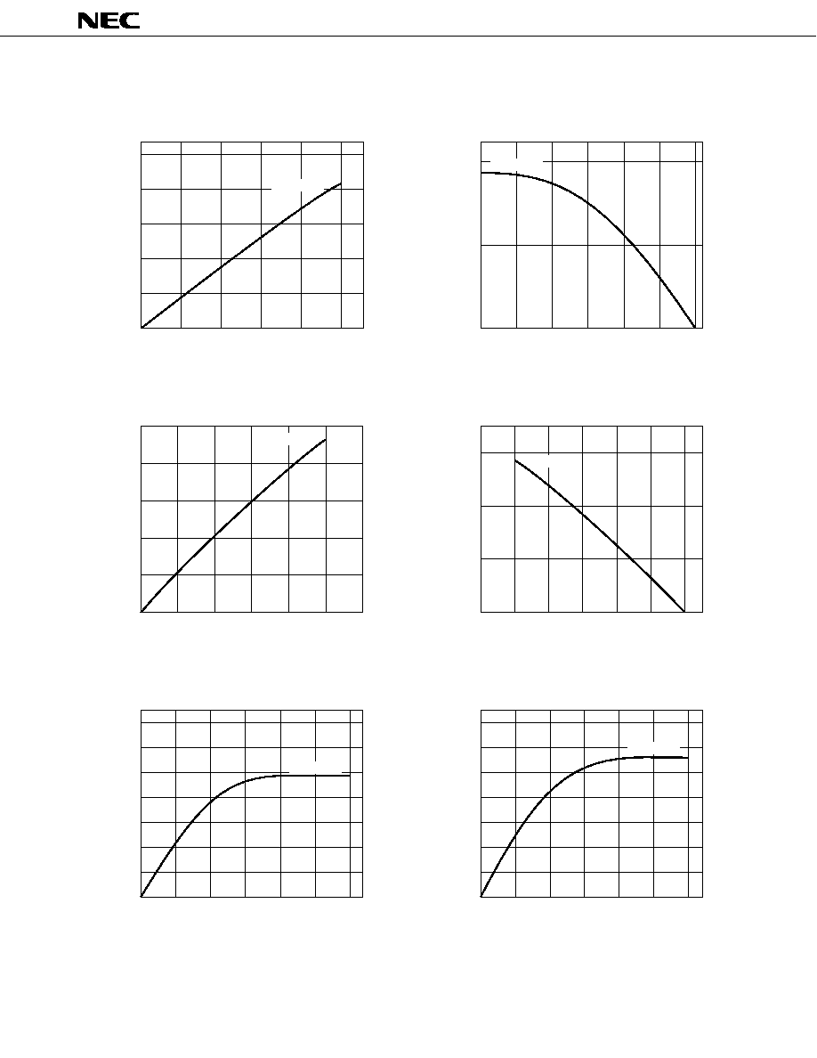
23. CHARACTERISTICS CURVE (REFERENCE VALUE) (Common in
µ
PD6124A and 6600A)
5.0
(T = 25 ± 3∞C)
A
0
0.2
Low-level output voltage V [V]
OL
I vs V characteristic examples (REM)
OL
OL
4.0
3.0
2.0
1.0
Low-level output current I [mA]
OL
0.4
0.6
0.8
1.0
(T = 25 ± 3∞C)
A
I vs V characteristic examples (REM)
OH
OH
≠10.0
≠5.0
High-level output current I [mA]
OH
0
0.5
High-level output voltage V [V]
OH
1.0
1.5
2.0
2.5
3.0
(T = 25 ± 3∞C)
A
I vs V characteristic examples (S-OUT)
OL
OL
(T = 25 ± 3∞C)
A
I vs V characteristic examples (S-OUT)
OH
OH
3.0
2.0
Low-level output current I [mA]
OL
4.0
5.0
1.0
0
0
≠2.0
High-level output current I [mA]
OH
≠1.0
≠3.0
0.2
low-level output voltage V [V]
OL
0.4
0.6
0.8
1.0
2.0
High-level output voltage V [V]
OH
2.2
2.4
2.6
2.8
3.0
(T = 25 ± 3∞C)
A
I vs V characteristic examples (K -K )
OL
OL
(T = 25 ± 3∞C)
A
I vs V characteristic examples (K -K )
OL
OL
50
Low-level output current I [ A]
OL
0
0
50
Low-level output current I [ A]
OL
Low-level output voltage V [V]
OL
1.0
2.0
3.0
Low-level output voltage V [V]
OL
1.0
2.0
3.0
µ
µ
I/O0
I/O3
I/O0
I/O7
V = 3 V
DD
V = 3 V
DD
V = 3 V
DD
V = 3 V
DD
V = 3 V
DD
V = 3 V
DD
µ
PD6124A, 6600A
28
(T = 25 ± 3∞C)
A
I vs V characteristic examples (K -K )
OH
OH
I/O0
I/O7
2.2
2.4
2.6
2.8
3.0
≠4.0
≠3.0
≠2.0
≠1.0
0
High-level output voltage V [V]
OH
High-level output current I [mA]
OH
V = 3 V
DD

µ
PD6124A, 6600A
29
24. PACKAGE DRAWINGS
20-Pin Plastic SOP (300 mil) (units in mm)
20 PIN PLASTIC SOP (300 mil)
ITEM
MILLIMETERS
INCHES
A
B
C
E
F
G
H
I
J
13.00 MAX.
1.27 (T.P.)
1.8 MAX.
1.55
7.7±0.3
0.78 MAX.
0.12
1.1
5.6
M
0.1±0.1
N
0.512 MAX.
0.031 MAX.
0.004±0.004
0.071 MAX.
0.061
0.303±0.012
0.220
0.043
0.005
0.050 (T.P.)
P20GM-50-300B, C-4
P
3
∞
3
∞
+7
∞
NOTE
Each lead centerline is located within 0.12 mm (0.005 inch) of
its true position (T.P.) at maximum material condition.
D
0.40
0.016
+0.10
≠0.05
K
0.20
0.008
+0.10
≠0.05
L
0.6±0.2
0.024
0.10
≠3
∞
+7
∞
≠3
∞
0.004
+0.008
≠0.009
+0.004
≠0.002
+0.004
≠0.003
A
C
D
G
P
detail of lead end
F
E
B
H
I
L
K
M
J
N
M
1
10
11
20

µ
PD6124A, 6600A
30
20PIN PLASTIC SHRINK DIP (300 mil)
ITEM
MILLIMETERS
INCHES
NOTES
1) Each lead centerline is located within 0.17 mm (0.007 inch) of
its true position (T.P.) at maximum material condition.
P20C-70-300B-1
N
0.17
0.007
R
0~15
∞
0~15
∞
A
19.57 MAX.
0.771 MAX.
B
1.78 MAX.
0.070 MAX.
F
0.85 MIN.
0.033 MIN.
G
3.2±0.3
0.126±0.012
J
5.08 MAX.
0.200 MAX.
K
7.62 (T.P.)
0.300 (T.P.)
C
1.778 (T.P.)
0.070 (T.P.)
D
0.50±0.10
0.020+0.004
≠0.005
H
0.51 MIN.
0.020 MIN.
I
4.31 MAX.
0.170 MAX.
L
6.5
0.256
M
0.25
0.010+0.004
≠0.003
+0.10
≠0.05
2) ltem "K" to center of leads when formed parallel.
M
R
M
I
H
G
F
D
N
C
B
K
1
10
20
11
A
L
J
µ
PD6124A, 6600A
31
fig.
20-PIN SHRINK DIP FOR ES (REFERENCE) (UNITS IN mm)
22.8
11.0
20
1
1.2
0.2
4.8
1.06
0.46
1.0
1.778
3.4
7.8

µ
PD6124A, 6600A
32
25. RECOMMENDED SOLDERING CONDITIONS
It is recommended that
µ
PD6124A and 6600A be soldered under the following conditions.
For details on the recommended soldering conditions, refer to Information Document "Semiconductor Device
Mounting Technology Manual" (C10535E).
For other soldering methods and conditions, consult NEC.
Table 25-1. Soldering Conditions of Surface-Mount Type
µ
PD6124AGS-XXX: 20-pin plastic SOP (300 mil)
µ
PD6600AGS-XXX: 20-pin plastic SOP (300 mil)
Symbol for
Soldering Method
Soldering Conditions
Recommended Condition
Infrared Reflow
Package peak temperature: 230
∞
C, time: 30 seconds max. (210
∞
C min.), number of times: 1
IR30-00-1
VPS
Package peak temperature: 215
∞
C, time: 40 seconds max. (200
∞
C min.), number of times: 1
VP15-00-1
Wave Soldering
Soldering bath temperature: 260
∞
C max., time: 10 seconds max., number of times: 1
Pre-heating temperature: 120
∞
C max. (package surface temperature)
WS60-00-1
Partial Heating
Pin temperature: 300
∞
C max., time: 3 seconds max. (per side)
≠
Caution
Do not use two or more soldering methods in combination (except the partial heating method).
Table 25-2. Soldering Conditions of Through-Hole Type
µ
PD6124ACS-XXX: 20-pin plastic shrink DIP (300 mil)
µ
PD6600ACS-XXX: 20-pin plastic shrink DIP (300 mil)
Soldering Method
Soldering Conditions
Wave Soldering (Only for pin part)
Soldering bath temperature: 260
∞
C max., time: 10 seconds max.
Partial Heating
Pin temperature: 300
∞
C max., time: 30 seconds max.
Caution
The wave soldering must be performed at the pin part only. Note that the solder must not be directly
contacted to the package body.

µ
PD6124A, 6600A
33
APPENDIX
µ
PD612
◊
SERIES PRODUCT LIST
Part Number
µ
PD6124A
µ
PD6600A
µ
PD61P24
µ
PD6125A
µ
PD6126A
Item
ROM capacity
1002
◊
10 bits
512
◊
10 bits
1002
◊
10 bits
1002
◊
10 bits
(mask ROM)
(mask ROM)
(one-time PROM)
(mask ROM)
RAM capacity
32
◊
5 bits
I/O pin
8 pins (K
I/O0-7
)
12 pins
16 pins (K
I/O0-7
,
(K
I/O0-7
, I/O
00-03
)
I/O
00-03
, I/O
10-13
)
S-IN pin
Provided
Current consumption
2
µ
A
1
µ
A
(f
OSC
= STOP) (MAX.)
S-IN high-level input
30
µ
A
15
µ
A
current (MAX.)
Transmission carrier frequency
f
OSC
/12, f
OSC
/8
Low-voltage detection
Provided
None
(reset) function
Mask option
Provided
None (fixed)
Provided
Supply voltage
V
DD
= 2.0 to 5.5 V V
DD
= 2.2 to 3.6 V V
DD
= 2.2 to 5.5 V V
DD
= 2.0 to 6.0 V
Package
∑ 20-pin plastic SOP (300 mil)
∑ 24-pin plastic
∑ 28-pin plastic
∑ 20-pin plastic shrink DIP (300 mil)
SOP (300 mil)
SOP (375 mil)
∑ 24-pin plastic
shrink DIP
(300 mil)

µ
PD6124A, 6600A
34
NOTES FOR CMOS DEVICES
1
PRECAUTION AGAINST ESD FOR SEMICONDUCTORS
Note: Strong electric field, when exposed to a MOS device, can cause destruction
of the gate oxide and ultimately degrade the device operation. Steps must
be taken to stop generation of static electricity as much as possible, and
quickly dissipate it once, when it has occurred. Environmental control must
be adequate. When it is dry, humidifier should be used. It is recommended
to avoid using insulators that easily build static electricity. Semiconductor
devices must be stored and transported in an anti-static container, static
shielding bag or conductive material. All test and measurement tools
including work bench and floor should be grounded. The operator should
be grounded using wrist strap. Semiconductor devices must not be touched
with bare hands. Similar precautions need to be taken for PW boards with
semiconductor devices on it.
2
HANDLING OF UNUSED INPUT PINS FOR CMOS
Note: No connection for CMOS device inputs can be cause of malfunction. If no
connection is provided to the input pins, it is possible that an internal input
level may be generated due to noise, etc., hence causing malfunction. CMOS
device behave differently than Bipolar or NMOS devices. Input levels of
CMOS devices must be fixed high or low by using a pull-up or pull-down
circuitry. Each unused pin should be connected to V
DD
or GND with a
resistor, if it is considered to have a possibility of being an output pin. All
handling related to the unused pins must be judged device by device and
related specifications governing the devices.
3
STATUS BEFORE INITIALIZATION OF MOS DEVICES
Note: Power-on does not necessarily define initial status of MOS device. Produc-
tion process of MOS does not define the initial operation status of the device.
Immediately after the power source is turned ON, the devices with reset
function have not yet been initialized. Hence, power-on does not guarantee
out-pin levels, I/O settings or contents of registers. Device is not initialized
until the reset signal is received. Reset operation must be executed imme-
diately after power-on for devices having reset function.

µ
PD6124A, 6600A
35
NEC Electronics Inc. (U.S.)
Santa Clara, California
Tel: 800-366-9782
Fax: 800-729-9288
NEC Electronics (Germany) GmbH
Duesseldorf, Germany
Tel: 0211-65 03 02
Fax: 0211-65 03 490
NEC Electronics (UK) Ltd.
Milton Keynes, UK
Tel: 01908-691-133
Fax: 01908-670-290
NEC Electronics Italiana s.r.1.
Milano, Italy
Tel: 02-66 75 41
Fax: 02-66 75 42 99
NEC Electronics Hong Kong Ltd.
Hong Kong
Tel: 2886-9318
Fax: 2886-9022/9044
NEC Electronics Hong Kong Ltd.
Seoul Branch
Seoul, Korea
Tel: 02-528-0303
Fax: 02-528-4411
NEC Electronics Singapore Pte. Ltd.
United Square, Singapore 1130
Tel: 253-8311
Fax: 250-3583
NEC Electronics Taiwan Ltd.
Taipei, Taiwan
Tel: 02-719-2377
Fax: 02-719-5951
NEC do Brasil S.A.
Sao Paulo-SP, Brasil
Tel: 011-889-1680
Fax: 011-889-1689
NEC Electronics (Germany) GmbH
Benelux Office
Eindhoven, The Netherlands
Tel: 040-2445845
Fax: 040-2444580
NEC Electronics (France) S.A.
Velizy-Villacoublay, France
Tel: 01-30-67 58 00
Fax: 01-30-67 58 99
NEC Electronics (France) S.A.
Spain Office
Madrid, Spain
Tel: 01-504-2787
Fax: 01-504-2860
NEC Electronics (Germany) GmbH
Scandinavia Office
Taeby, Sweden
Tel: 08-63 80 820
Fax: 08-63 80 388
Regional Information
Some information contained in this document may vary from country to country. Before using any NEC
product in your application, please contact the NEC office in your country to obtain a list of authorized
representatives and distributors. They will verify:
∑ Device availability
∑ Ordering information
∑ Product release schedule
∑ Availability of related technical literature
∑ Development environment specifications (for example, specifications for third-party tools and
components, host computers, power plugs, AC supply voltages, and so forth)
∑ Network requirements
In addition, trademarks, registered trademarks, export restrictions, and other legal issues may also vary
from country to country.
J96. 8

µ
PD6124A, 6600A
[MEMO]
The export of this product from Japan is regulated by the Japanese government. To export this product may be prohibited
without governmental license, the need for which must be judged by the customer. The export or re-export of this product
from a country other than Japan may also be prohibited without a license from that country. Please call an NEC sales
representative.
The application circuits and their parameters are for reference only and are not intended for use in actual design-ins.
No part of this document may be copied or reproduced in any form or by any means without the prior written
consent of NEC Corporation. NEC Corporation assumes no responsibility for any errors which may appear in
this document.
NEC Corporation does not assume any liability for infringement of patents, copyrights or other intellectual property
rights of third parties by or arising from use of a device described herein or any other liability arising from use
of such device. No license, either express, implied or otherwise, is granted under any patents, copyrights or other
intellectual property rights of NEC Corporation or others.
While NEC Corporation has been making continuous effort to enhance the reliability of its semiconductor devices,
the possibility of defects cannot be eliminated entirely. To minimize risks of damage or injury to persons or
property arising from a defect in an NEC semiconductor device, customers must incorporate sufficient safety
measures in its design, such as redundancy, fire-containment, and anti-failure features.
NEC devices are classified into the following three quality grades:
"Standard", "Special", and "Specific". The Specific quality grade applies only to devices developed based on a
customer designated "quality assurance program" for a specific application. The recommended applications of
a device depend on its quality grade, as indicated below. Customers must check the quality grade of each device
before using it in a particular application.
Standard: Computers, office equipment, communications equipment, test and measurement equipment,
audio and visual equipment, home electronic appliances, machine tools, personal electronic
equipment and industrial robots
Special:
Transportation equipment (automobiles, trains, ships, etc.), traffic control systems, anti-disaster
systems, anti-crime systems, safety equipment and medical equipment (not specifically designed
for life support)
Specific:
Aircrafts, aerospace equipment, submersible repeaters, nuclear reactor control systems, life
support systems or medical equipment for life support, etc.
The quality grade of NEC devices is "Standard" unless otherwise specified in NEC's Data Sheets or Data Books.
If customers intend to use NEC devices for applications other than those specified for Standard quality grade,
they should contact an NEC sales representative in advance.
Anti-radioactive design is not implemented in this product.
M4 96.5