 | –≠–ª–µ–∫—Ç—Ä–æ–Ω–Ω—ã–π –∫–æ–º–ø–æ–Ω–µ–Ω—Ç: UPD6345GS | –°–∫–∞—á–∞—Ç—å:  PDF PDF  ZIP ZIP |

©
1995
DATA SHEET
The
µ
PD6345 is a monolithic Bi-CMOS integrated Circuit designed to drive LED, Solenoid and Relay.
This device consists of an 8-bit shift register, latch and buffer with high voltage N-P-N Transistors (Open Collector).
Data is serially loaded into shift register on the positive-going transition of the clock. Parallel data is transferred to
the output buffers through the 8-bit latch while the latch enable input is high and latched when the latch enable is low.
When the output enable input is low, all outputs are off (High Impedance).
FEATURES
∑
High Speed Serially-shifted Data Input.
∑
Latches on all driver Outputs.
∑
40 V Output Voltage Rating.
∑
60 mA Output Sink Current.
∑
Built in power supply voltage detection circuit.
∑
Capable of connection to cascade additional device.
∑
Wide Operating Temperature Range: ≠40 to +85
∞
C
∑
Bi-CMOS STRUCTURE
ORDERING INFORMATION
Part Number
Package
µ
PD6345C
16 Pin Plastic DIP (300 mil)
µ
PD6345GS
16 Pin Plastic SOP (300 mil)
MOS INTEGRATED CIRCUIT
µ
PD6345
8 BIT SERIAL IN/PARALLEL OUT DRIVER
1988
Document No. IC-2166A (2nd edition)
(O.D. No. IC-5437A)
Date Published March 1997 P
Printed in Japan
µ
PD6345
2
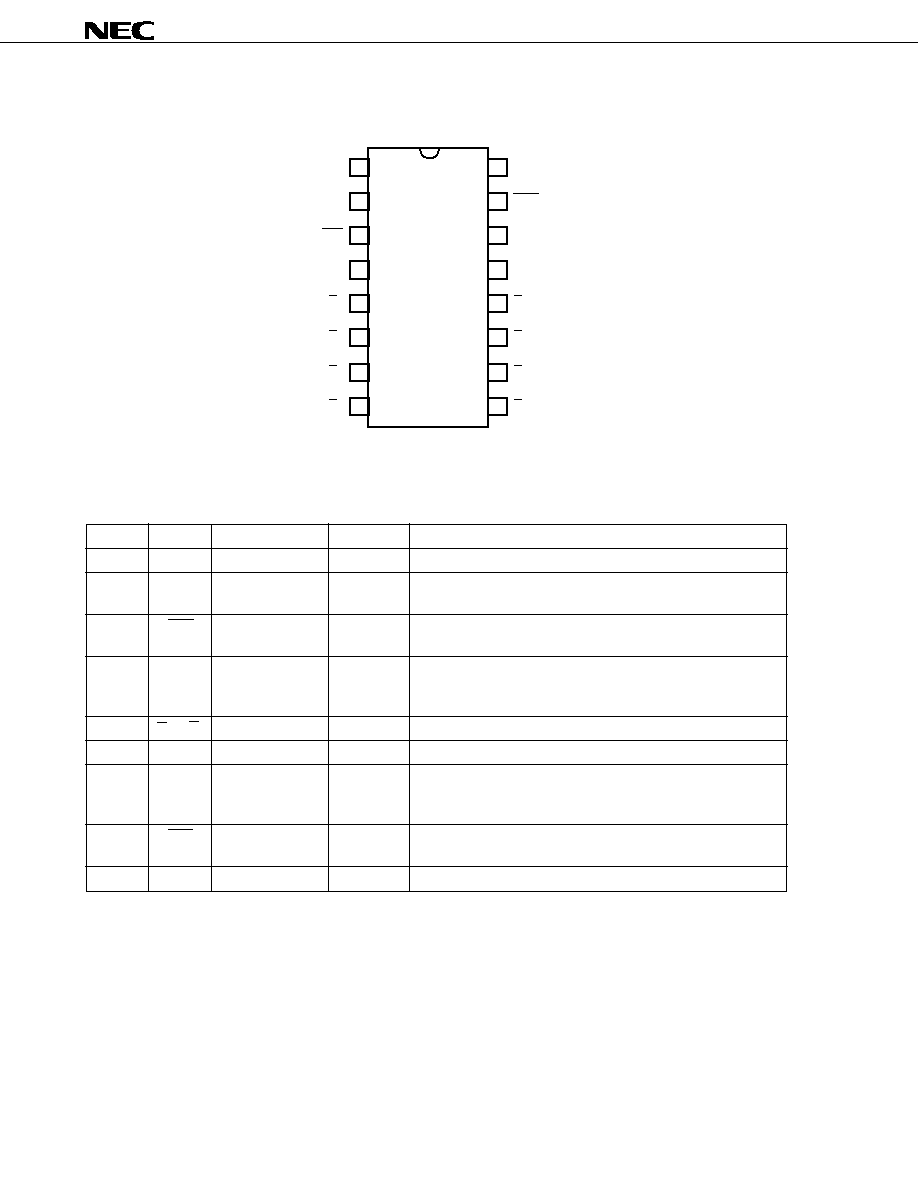
PIN CONFIGURATION (Top View)
PIN IDENTIFICATION
Pin No.
Symbol
Pin name
Input/Output
Function
1
GND
Ground
--
Connection to Ground (GND) of system.
2
EN
Output Enable
Input
When this pin is low or open, all outputs are OFF, and data is output
during high.
3
LAT
Latch Enable
Input
When this pin is low or open, data is latched and data is through to
output during high.
4
SO
Serial data Output
Output
Serial data is output on positive-going transition of the clock.
In case of connection to cascade additional device (
µ
PD6345), this
pin will be connected to SIN terminal of additional device.
5 to 12
O
8
to O
1
Driver Output
Output
High Voltage and Current Driver Outputs.
13
SIN
Serial data Input
Input
Data is loaded to shift register on positive-going transition.
14
SCK
Clock
Input
Data of SIN is loaded to shift register on positive-going transition of
SCK. Also, serial data is output from SO on positive-going transition
of SCK.
15
RES
Reset
Input
When this pin is low or open, data of shift register is all cleared, and
this device operate normally during high.
16
V
DD
Power Supply
--
Normally supply 5 V.
1
2
3
4
5
6
7
8
16
15
14
13
12
11
10
9
V
SS
EN
LAT
SO
O
8
O
7
O
6
O
5
V
DD
RES
SCK
SIN
O
1
O
2
O
3
O
4
3
µ
PD6345
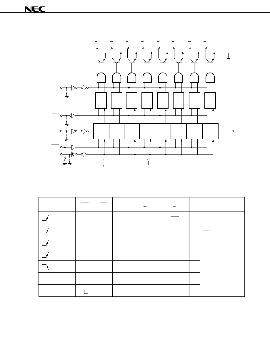
TRUTH TABLE
SCK
EN
RES
LAT
SIN
OUT
SO
*1
Note
O
1
O
n
H
H
H
L
High Impedance
O
n ≠ 1
S
7
H
H
H
H
L
O
n ≠ 1
S
7
H
H
L
*2
*
NO CHANGE
NO CHANGE
S
7
L
H
*
*
High Impedance High Impedance
S
7
*
*
*
*
NO CHANGE
NO CHANGE
S
8
*
*
L
H
*
High Impedance High Impedance
L
*
H
L
*
NO CHANGE
NO CHANGE
L
*1) Seventh data S
7
of shift register is loaded to eighth data S
8
on positive-going transition of clock, and is output
to Serial data Output pin.
*2) Shift register operates normally.
BLOCK DIAGRAM
O
1
O
2
O
3
O
4
O
5
O
6
O
7
O
8
P
1
P
2
P
3
P
4
P
5
P
6
P
7
P
8
S
1
S
2
S
3
S
4
S
5
S
6
S
7
S
8
SO
EN
LAT
SIN
RES
SCK
100 k
100 k
100 k
100 k
100 k
P
1
to P
8
; Latch Circuits
S
1
to S
8
; 8-bit Shift register
SCK = CLOCK
EN = Output Enable
RES= Reset
LAT= Latch Enable
SIN = Serial data Input
OUT = Driver Output
SO = Serial data Output
* = H or L
H = High level
L = Low level
µ
PD6345
4
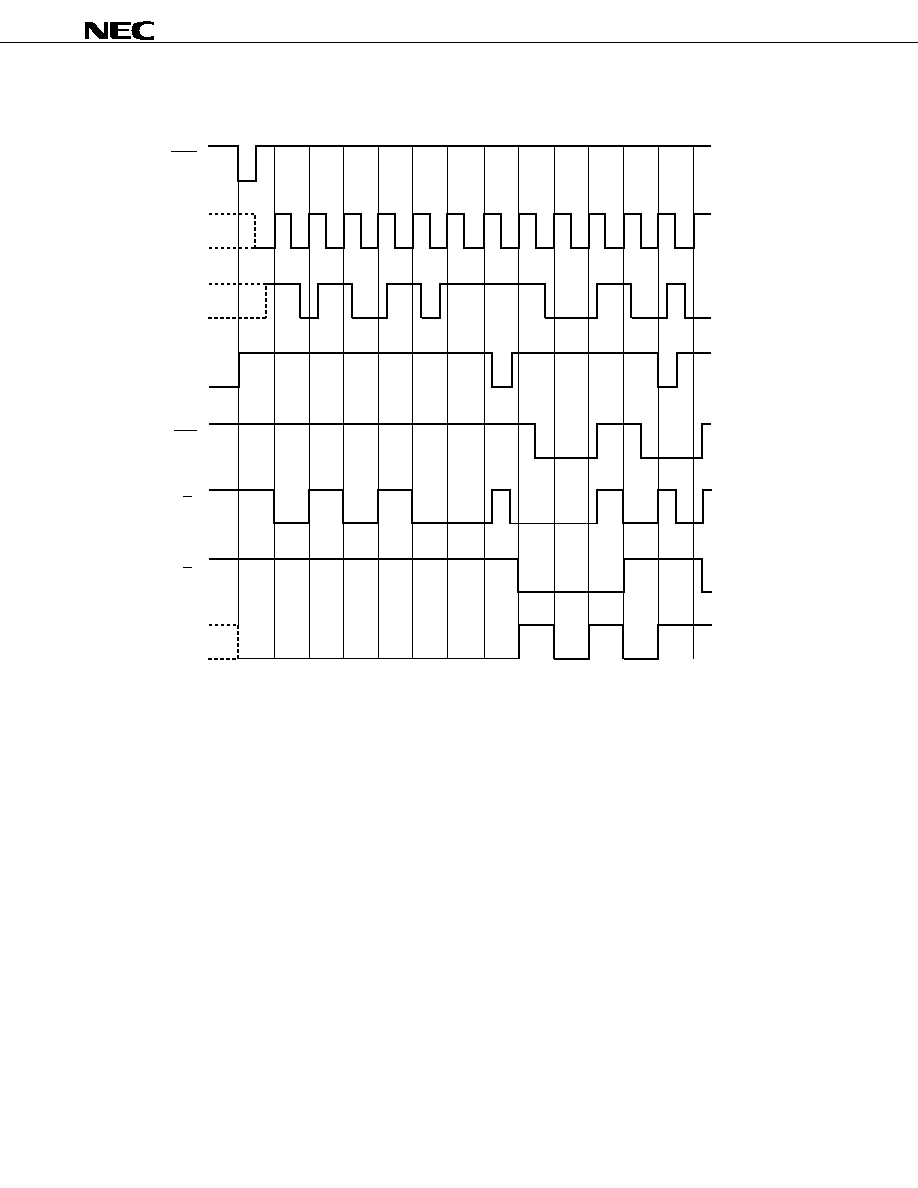
TIMING CHART
RES
SCK
SIN
EN
LAT
O
1
O
8
SO

5
µ
PD6345
ABSOLUTE MAXIMUM RATINGS (T
a
= 25
∞
C
±
2
∞
C)
Supply Voltage
V
DD
≠0.3 to 7.0
V
Input Voltage
V
IN
≠0.3 to V
DD
+ 0.3
V
Input Current
V
IN
±
10
mA
Logic Output Voltage
V
SO1
≠0.3 to V
DD
+ 0.3
V
Driver Output Voltage
V
OUT2
≠0.3 to 40
V
Driver Output Current
I
OUT
100
mA
Logic Output Current
I
SO
+10
mA
≠5
Power Dissipation
P
D
850 (DIP), 800 (SOP)
mW
Operating Temperature
T
opt
≠40 to + 85
∞
C
Storage Temperature
T
stg
≠55 to +150
∞
C
RECOMMENDED OPERATING CONDITIONS
ITEM
SYMBOL
MIN.
TYP.
MAX.
UNIT
Operating Temperature
T
opt
≠40
+85
∞
C
Supply Voltage
V
DD
4.0
5.0
6.0
V
Input Voltage
V
IN
0
V
DD
V
High Level Input Voltage
V
IH
0.7 V
DD
V
DD
V
Low Level Input Voltage
V
IL
0
0.2 V
DD
V
Clock Frequency
f
SCK
8
MHz
Driver Output Voltage
V
OUT
0
38
V
µ
PD6345
6
ELECTRICAL CHARACTERISTICS (RH
70 %, V
SS
= 0 V)
ITEM
SYMBOL
CONDITION
T
a
= 25
∞
C
T
a
= ≠40 to +85
∞
C
UNIT
V
DD
(V)
MIN. TYP. MAX. MIN. TYP. MAX.
High Level Input Voltage
V
IH
5.0
3.5
2.4
3.5
V
6.0
4.2
4.2
Low Level Input Voltage
V
IL
5.0
1.7
1.0
1.0
V
6.0
1.2
1.2
High Level Input Current
I
IH
6.0
V
IN
= V
DD
100
300
300
µ
A
Low Level Input Current
I
IL
6.0
V
IN
= V
SS
0.03
0.3
1
µ
A
High Level Output Voltage 1
V
SOH1
5.0
I
SOH
= ≠250
µ
A
3.6
3.6
V
6.0
I
SOH
= ≠300
µ
A
4.3
4.3
High Level Output Voltage 2
V
SOH2
5.0
I
SOH
= ≠10
µ
A
4.0
4.0
V
6.0
5.0
5.0
High Level Output Voltage 3
V
SOH3
5.0
I
SOH
= ≠1
µ
A
3.3
3.3
V
6.0
4.0
4.0
Low Level Output Voltage
V
SOL
5.0
I
SOL
= 8
µ
A
0.6
V
6.0
0.5
Low Level Output Voltage (Driver)
V
OUT(L)
5.0
I
OUT
= 60
µ
A
0.45
0.8
1.0
V
High Level Output Leakage Current
I
OHL
5.0
10
10
µ
A
Supply Current
I
DD1
5.0
O
1
≠ O
8
0.25
0.5
1.0
mA
I
DD2
5.0
23
35
40
Input Capacitance
C
IN
--
6
15
15
pF

7
µ
PD6345
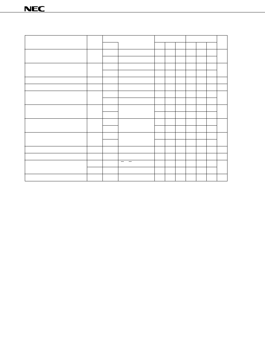
SWITCHING CHARACTERISTICS
(T
a
= 25
∞
C, V
DD
= 5 V, C
L
= 15 pF, R (O
n
) = 300
, V
OUT
= 12 V, t
r
= t
f
= 6 ns)
ITEM
SYMBOL
CONDITION
MIN.
TYP.
MAX.
UNIT
t
PLH1
SCK
SO (High Level)
20
100
ns
t
PLH2
SCK
Driver Output (High Level)
20
1
µ
s
t
PHL1
SCK
SO (Low Level)
100
ns
Propagation Delay Time
t
PHL2
SCK
Driver Output (Low Level)
1
µ
s
t
PHL3
RESET
SO
100
ns
t
PHL/PLH4
Output Enable
Driver Output
1
µ
s
t
PHL/PLH5
Latch Enable
Driver Output
1
µ
s
Clock Transition Time
t
r
SCK
70
µ
s
t
f
Maximum Clock Frequency
f
max
13
8
MHz
Minimum Data Setup Time
t
SETUP
20
10
ns
Minimum Data Hold Time
t
HOLD
20
10
ns
Minimum Reset Pulse Width
PW
RESET
62.5
10
ns
Minimum Output Enable Pulse Width PW
ENABLE
1
0.55
µ
s
Minimum Latch Enable Pulse Width
PW
LATCH
62.5
38
ns
Clock Pulse Width
PW
SCK
38
62.5
ns
µ
PD6345
8
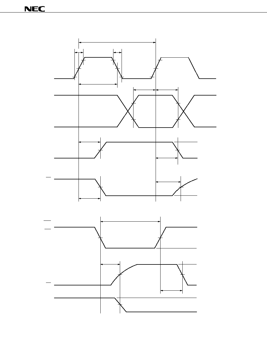
TIMING WAVEFORMS
SCK
SIN
SO
Qn
RES
EN
LAT
On
SO
10 %
10 %
90 %
50 %
90 %
50 %
50 %
50 %
50 %
50 %
50 %
50 %
1/f
max.
t
r
t
r
PW
CLOCK
t
SETUP
t
HOLD
t
PLH1
t
PHL2
t
PHL1
t
PLH2
50 %
50 %
PW
50 %
50 %
t
PLH3
to
5
50 %
50 %
t
PHL4
to
5
50 %
V
OH
V
OL
High Impedance
V
OL
V
OH
V
OL
High Impedance
V
OL
V
OH
V
OL
9
µ
PD6345
TYPICAL CHARACTERISTICS (T
a
= 25
∞
C)
DRIVER OUTPUT CHARACTERISTICS
100
80
60
40
20
0
0
0.2
0.4
0.6
0.8
1.0
V
DD
= 6 V
V
DD
= 5 V
V
DD
= 4 V
Driver Output Voltage V
OUT
(L) (V)
Driver Output Current I
OUT
(mA)
0.8
0.6
0.4
0.2
≠40
Ambient Temperature T
a
(∞C)
Driver Output Voltage V
OUT
(L) (V)
≠20
0
20
40
60
85
V
DD
= 5V
I
OUT
= 60 mA

µ
PD6345
10
SUPPLY CURRENT CHARACTERISTICS (8 Outputs is all ON, No load)
40
30
20
10
0
4.0
5.0
6.0
Supply Voltage V
DD
(V)
Supply Current I
DD
(mA)
0
≠40
Ambient Temperature T
a
(∞C)
Supply Current I
DD
(mA)
10
20
30
40
≠20
0
20
40
60
80
11
µ
PD6345
PACKAGE POWER DISSIPATION CHARACTERISTICS
800
600
400
200
0
0
25
40
60
85
100
Ambient Temperature T
a
(∞C)
Power Dissipation P
D
(mW)
PD6345 (DIP)
µ
800
600
400
200
0
0
25
40
60
85
100
Ambient Temperature T
a
(∞C)
Power Dissipation P
D
(mW)
PD6345 (SOP)
µ
µ
PD6345
12
APPLICATION CIRCUIT
(1) Driving of Solenoid
(2) Driving of Solenoid for High Current
to 40 V
+5 V
EN
LAT
SIN
SCK
RES
EN
LAT
SO
SCK
RES
V
DD
V
DD
O
1
O
2
O
8
1 chip
CPU
V
SS
V
SS
µ
PD6345
Solenoid
(to 60 mA)
V
CC
V
DD
to 40 V
+5 V
V
CC
V
DD
Solenoid
(a few Ampere)
R
T
r
T
r
R
R
T
r
EN
LAT
SIN
SCK
RES
V
DD
O
1
O
2
O
8
V
SS
µ
PD6345
1 chip
CPU
V
DD
V
SS
EN
LAT
SO
SCK
RES
13
µ
PD6345
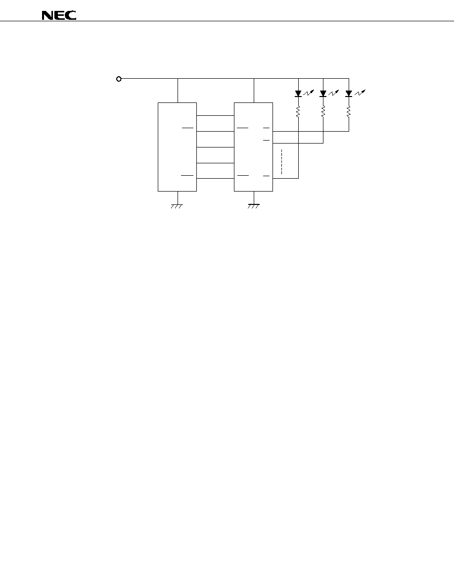
(2) Driving of LED
V
DD
(5 V)
R
R
R
EN
LAT
SIN
SCK
RES
EN
LAT
SO
SCK
RES
V
DD
V
DD
O
1
O
2
O
8
1 chip CPU
µ
PD6345

µ
PD6345
14
16PIN PLASTIC DIP (300 mil)
P16C-100-300A,C-1
ITEM
MILLIMETERS
INCHES
NOTES
1) Each lead centerline is located within 0.25 mm (0.01 inch) of
its true position (T.P.) at maximum material condition.
A
B
1.27 MAX.
20.32 MAX.
0.800 MAX.
0.050 MAX.
C
2.54 (T.P.)
0.100 (T.P.)
N
0.25
0.01
P
R
0~15
∞
1.0 MIN.
0.039 MIN.
0~15
∞
2) Item "K" to center of leads when formed parallel.
M
0.25
0.010 +0.004
≠0.003
F
1.2 MIN.
0.047 MIN.
G
H
0.51 MIN.
3.5±0.3
0.138±0.012
0.020 MIN.
I
4.31 MAX.
0.170 MAX.
J
K
7.62 (T.P.)
5.08 MAX.
0.200 MAX.
0.300 (T.P.)
L
6.4
0.252
+0.10
≠0.05
M
R
M
I
G
H
F
B
N
C
D
D
0.50±0.10
0.020+0.004
≠0.005
P
16
9
1
8
A
J
K
L

15
µ
PD6345
16 PIN PLASTIC SOP (300 mil)
ITEM
MILLIMETERS
INCHES
A
B
C
E
F
G
H
I
J
10.46 MAX.
1.27 (T.P.)
1.8 MAX.
1.55
7.7±0.3
0.78 MAX.
0.12
1.1
5.6
M
0.1±0.1
N
0.412 MAX.
0.031 MAX.
0.004±0.004
0.071 MAX.
0.061
0.303±0.012
0.220
0.043
0.005
0.050 (T.P.)
P16GM-50-300B-4
P
3
∞
3
∞
+7
∞
NOTE
Each lead centerline is located within 0.12 mm (0.005 inch) of
its true position (T.P.) at maximum material condition.
D
0.40
0.016
+0.10
≠0.05
K
0.20
0.008
+0.10
≠0.05
L
0.6±0.2
0.024
0.10
≠3
∞
+7
∞
≠3
∞
0.004
+0.008
≠0.009
+0.004
≠0.002
+0.004
≠0.003
A
C
D
G
P
detail of lead end
F
E
B
H
I
L
K
M
M
1
8
9
16
J
N

µ
PD6345
16
[MEMO]
No part of this document may be copied or reproduced in any form or by any means without the prior written
consent of NEC Corporation. NEC Corporation assumes no responsibility for any errors which may appear in
this document.
NEC Corporation does not assume any liability for infringement of patents, copyrights or other intellectual property
rights of third parties by or arising from use of a device described herein or any other liability arising from use
of such device. No license, either express, implied or otherwise, is granted under any patents, copyrights or other
intellectual property rights of NEC Corporation or others.
While NEC Corporation has been making continuous effort to enhance the reliability of its semiconductor devices,
the possibility of defects cannot be eliminated entirely. To minimize risks of damage or injury to persons or
property arising from a defect in an NEC semiconductor device, customers must incorporate sufficient safety
measures in its design, such as redundancy, fire-containment, and anti-failure features.
NEC devices are classified into the following three quality grades:
"Standard", "Special", and "Specific". The Specific quality grade applies only to devices developed based on a
customer designated "quality assurance program" for a specific application. The recommended applications of
a device depend on its quality grade, as indicated below. Customers must check the quality grade of each device
before using it in a particular application.
Standard: Computers, office equipment, communications equipment, test and measurement equipment,
audio and visual equipment, home electronic appliances, machine tools, personal electronic
equipment and industrial robots
Special:
Transportation equipment (automobiles, trains, ships, etc.), traffic control systems, anti-disaster
systems, anti-crime systems, safety equipment and medical equipment (not specifically designed
for life support)
Specific:
Aircrafts, aerospace equipment, submersible repeaters, nuclear reactor control systems, life
support systems or medical equipment for life support, etc.
The quality grade of NEC devices is "Standard" unless otherwise specified in NEC's Data Sheets or Data Books.
If customers intend to use NEC devices for applications other than those specified for Standard quality grade,
they should contact an NEC sales representative in advance.
Anti-radioactive design is not implemented in this product.
M4 96.5