 | –≠–ª–µ–∫—Ç—Ä–æ–Ω–Ω—ã–π –∫–æ–º–ø–æ–Ω–µ–Ω—Ç: UPD98409 | –°–∫–∞—á–∞—Ç—å:  PDF PDF  ZIP ZIP |
Document Outline
- COVER
- DESCRIPTION
- FEATURES
- ORDERING INFORMATION
- EXAMPLE OF SYSTEM CONFIGURATION
- BLOCK DIAGRAM
- PIN CONFIGURATION (Top View)
- PIN NAMES
- 1. PIN FUNCTION
- 1.1 PHY Device Interface Pin
- 1.1.1 UTOPIA interface
- 1.1.2 PHY device control interface
- 1.2 Bus Interface Pins
- 1.3 Serial EEPROM Interface Pins
- 1.4 JTAG Boundary Scan Pins
- 1.5 Other Pins
- 1.6 Power and Ground Pins
- 2. ELECTRICAL SPECIFICATIONS
- 3. PACKAGE DRAWING
- 4. SOLDERING CONDITIONS
The information in this document is subject to change without notice.
MOS INTEGRATED CIRCUIT
µ
µ
µ
µ
PD98409
ATM LIGHT SAR CONTROLLER
1997, 1998
©
Document No. S12775EJ2V0DS00 (2nd edition)
Date Published May 1998 N CP(K)
Printed in Japan
DATA SHEET
The mark shows major revised points.
DESCRIPTION
The
µ
PD98409 (NEASCOT-S40C
TM
) is a high-performance SAR chip for segmentation and reassembly of ATM
cells. Provided with a PCI (Peripheral Component Interconnect) bus interface control memory and supporting a
MPEG packet transfer engine function to mitigate the workload of the CPU in transferring compressed image data,
this chip has ideal specifications for use in a set top box (STB) to interface with an ATM network. The
µ
PD98409
conforms to ATM Forum recommendations and has AAL5-SAR sublayer and ATM layer functions.
FEATURES
∑
Conforms to ATM Forum
∑
PCI bus interface (5/3.3 V, 32/64 bits, 33 MHz)
Conforms to PCI Local Bus Specification Revision 2.1
∑
AAL-5 SAR sublayer and ATM layer functions
∑
Hardware support of AAL-5 processing (non-AAL-5 processing can be supported in software)
∑
Supports up to 64 virtual channels (VC) (64-VC control memory)
∑
Two traffic shapers for transmission scheduling
∑
MPEG packet transfer engine mitigating the workload of compressed image data transfer by CPU
∑
Receive FIFO of 12 cells
∑
PHY device I/F: UTOPIA Level-1 interface (octet/cell level handshake)
∑
JTAG boundary scan test functions
∑
0.35-
µ
m CMOS process, +5/+3.3-V power supply
- Bus interface +5 V : +5/+3.3-V power supply
- Bus interface +3.3 V : +3.3-V single power supply
ORDERING INFORMATION
Part Number
Package
µ
PD98409GN-LMU
240-pin plastic QFP (0.5-mm fine pitch) (32
◊
32 mm)
2
µ
µ
µ
µ
PD98409
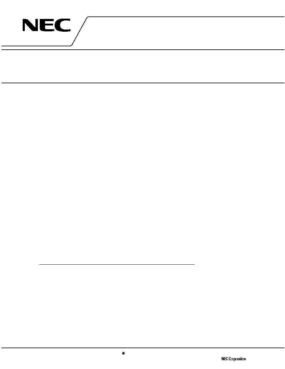
EXAMPLE OF SYSTEM CONFIGURATION
µ
PD98409
CPU
Memory
ATM STB
PCI bus
Line interface
MPEG decoder
block
BLOCK DIAGRAM
PCI
interface
DMA
controller
Receive
PHY
interface
Rx UTOPIA interface
PHY control interface
Tx UTOPIA interface
Transmit
PHY
interface
Control
memory
(64 VCs)
Control
memory
interface
MPEG
packet
transfer
engine
PCI
interface
block
Receive data FIFO (12 cells)
Transmit data FIFO (2 cells)
Transmit controller
Sequencer
Receive controller
3
µ
µ
µ
µ
PD98409
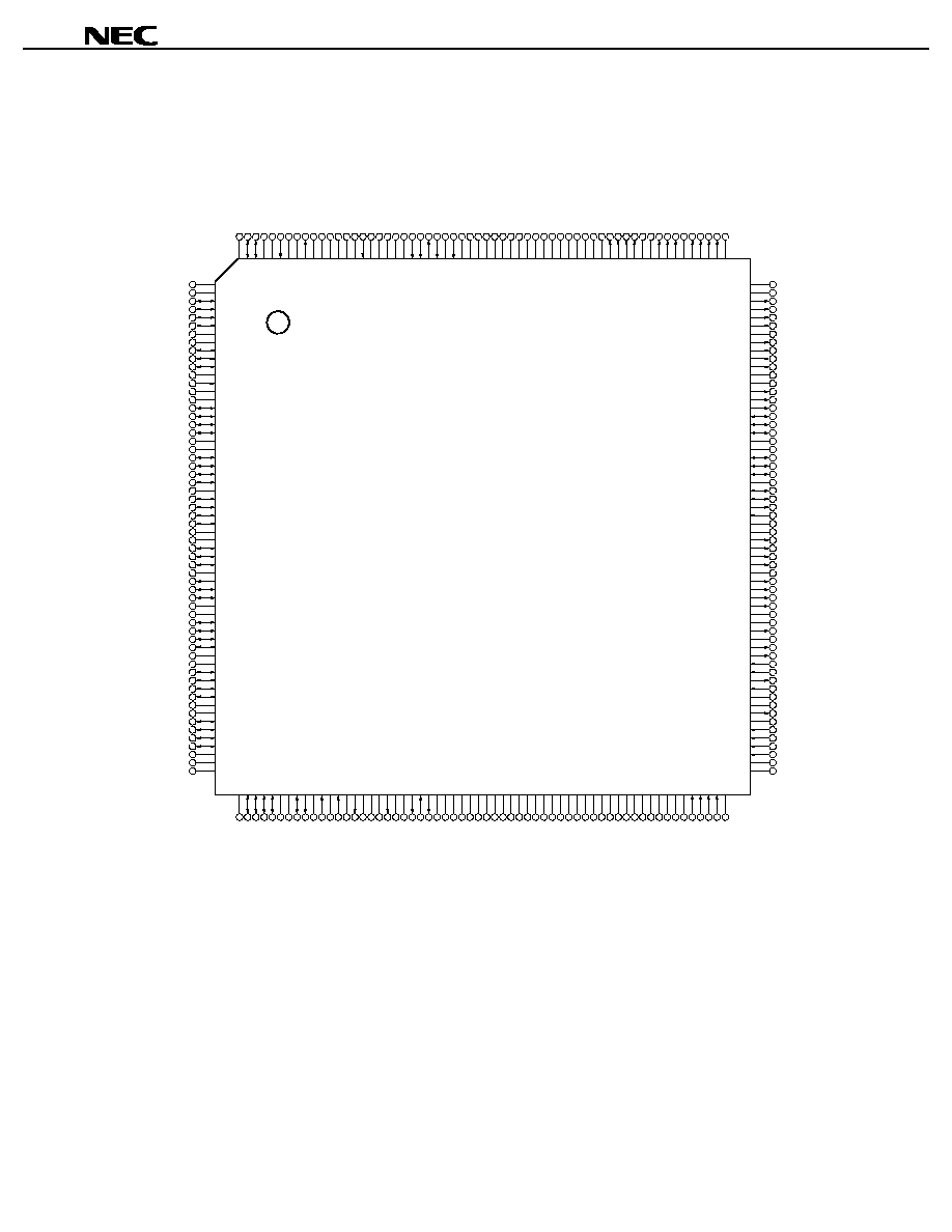
PIN CONFIGURATION (Top View)
∑ 240-pin plastic QFP (0.5-mm fine pitch) (32
◊
◊
◊
◊
32 mm)
GND
GND
60
1
GND
2
AD29
3
AD28
4
AD27
5
AD26
6
GND
7
VDD5
8
AD25
9
AD24
10
PCBE3_B
11
GND
12
IDSEL
13
VDD5
14
GND
15
AD23
16
AD22
17
AD21
18
AD20
19
GND
20
VDD3
21
AD19
22
AD18
23
AD17
24
AD16
25
GND
26
PCBE2_B
27
FRAME_B
28
IRDY_B
29
TRDY_B
30
GND
31
VDD5
32
DEVSEL_B
33
STOP_B
34
PERR_B
35
GND
36
SERR_B
37
PAR
38
PCBE1_B
39
VDD3
40
GND
41
AD15
42
AD14
43
AD13
44
AD12
45
GND
46
VDD5
47
AD11
48
AD10
49
AD9
50
AD8
51
VDD5
52
GND
53
PCBE0_B
54
AD7
55
AD6
56
AD5
57
VDD5
58
GND
59
VDD3
VDD3
120
61
AD4
62
AD3
63
AD2
64
AD1
65
GND
66
VDD5
67
AD0
68
REQ_B
69
GND
70
GNT_B
71
GND
72
BUSCLK
73
GND
74
INTR_B
75
VDD5
76
GND
77
GND
78
E2PCLK
79
GND
80
VDD3
81
E2PDO
82
E2PDI
83
E2PCS
84
GND
85
IC
86
IC
87
IC
88
IC
89
GND
90
VDD3
91
IC
92
IC
93
IC
94
IC
95
GND
96
IC
97
GND
98
IC
99
VDD3
100
GND
101
IC
102
IC
103
IC
104
IC
105
IC
106
IC
107
IC
108
IC
109
GND
110
IC
111
GND
112
IC
113
IC
114
IC
115
RX7
116
RX6
117
RX5
118
RX4
119
GND
GND
121
180
GND
179
CA8
178
CA7
177
CA6
176
CA5
175
GND
174
CA4
173
CA3
172
CA2
171
CA1
170
VDD3
169
GND
168
CA0
167
PHCE_B
166
PHOE_B
165
CD0
164
CD1
163
CD2
162
GND
161
VDD3
160
CD3
159
CD4
158
CD5
157
GND
156
CD6
155
CD7
154
PHRW_B
153
PHINT_B
152
VDD3
151
GND
150
TX0
149
TX1
148
TX2
147
TX3
146
GND
145
TX4
144
TX5
143
TX6
142
TX7
141
VDD3
140
GND
139
TCLK
138
GND
137
TENBL_B
136
TSOC
135
FULL_B/TXCLAV
134
RSOC
133
RENBL_B
132
EMPTY_B/RXCLAV
131
VDD3
130
GND
129
RCLK
128
GND
127
RX0
126
RX1
125
RX2
124
RX3
123
GND
122
VDD3
VDD3
181
240
AD30
239
AD31
238
VDD5
237
GND
236
RST_B
235
VDD5
234
GND
233
RSTOUT_B
232
IC
231
IC
230
IC
229
GND
228
IC
227
IC
226
PHYSEL1
225
IC
224
GND
223
NC
222
GND
221
VDD3
220
JRST_B
219
JMS
218
JDO
217
JDI
216
GND
215
JCK
214
GND
213
IC
212
IC
211
IC
210
IC
209
IC
208
GND
207
VDD3
206
IC
205
IC
204
IC
203
IC
202
VDD3
201
GND
200
IC
199
L
198
L
197
GND
196
PO0
195
PO1
194
PO2
193
PO3
192
GND
191
VDD3
190
LASTB
189
LA0
188
LA1
187
GND
186
LA2
185
LA3
184
LA4
183
LA5
182
PD98409GN-LMU
µ
NC : No connection. Leave this pin open.
IC : Input pin with pull-down resistor for internal test. It is recommended to fix this pin to the low level.
L
: Fix this pin to the low level.

4
µ
µ
µ
µ
PD98409
PIN NAMES
AD31_AD0
: Address/Data
PHINT_B
: PHY Interrupt
BUSCLK
: Bus Clock
PHOE_B
: PHY Output Enable
CA8-CA0
: PHY Device Address
PHRW_B
: PHY Read/Write
CD7-CD0
: PHY Device Data
PHYSEL1
: PHY Select
DEVSEL_B
: Device Select
PO3-PO0
: Generic Output Port
E2PCLK
: Clock for EEPROM
TM
RCLK
: Receive Clock
E2PCS
: EEPROM Chip Select
RENBL_B
: Receive Enable
E2PDI
: Serial Data Input from EEPROM
REQ_B
: Request
E2PDO
: Serial Data Output to EEPROM
RSOC
: Receive Start of Cell
EMPTY_B/RxCLAV: PHY Empty / Rx Cell Available
RST_B
: Reset
FRAME_B
: Cycle Frame
RSTOUT_B
: Reset Output
FULL_B/TxCLAV
: PHY Buffer Full / Tx Cell Available
Rx7-Rx0
: Receive Data Bus
GND
: Ground
SERR_B
: System Error
GNT_B
: Grant
STOP_B
: Stop
IDSEL
: ID Select
TCLK
: Transmit Clock
INTR_B
: Interrupt
TENBL_B
: Transmit Enable
IRDY_B
: Initiator Ready
TRDY_B
: Target Ready
JCK
: JTAG Test Pin
TSOC
: Transmit Start of Cell
JDI
: JTAG Test Pin
Tx7-Tx0
: Transmit Data Bus
JDO
: JTAG Test Pin
V
DD3
: +3.3 V Power Supply
JMS
: JTAG Test Pin
V
DD5
: +5 V Power Supply
JRST_B
: JTAG Test Pin
LA5-LA0
: Internal Test Pin
LASTB
: Internal Test Pin
PAR
: Parity
PCBE_B3-PCBE_B0: Bus Command and Byte Enables
PERR_B
: Parity Error
PHCE_B
: PHY Chip Enable

5
µ
µ
µ
µ
PD98409
CONTENTS
1. PIN FUNCTION ...................................................................................................................................... 6
1.1 PHY Device Interface Pin............................................................................................................................... 6
1.1.1 UTOPIA interface................................................................................................................................. 6
1.1.2 PHY device control interface ............................................................................................................. 7
1.2 Bus Interface Pins.......................................................................................................................................... 8
1.3 Serial EEPROM Interface Pins .................................................................................................................... 10
1.4 JTAG Boundary Scan Pins.......................................................................................................................... 10
1.5 Other Pins ..................................................................................................................................................... 11
1.6 Power and Ground Pins .............................................................................................................................. 11
2. ELECTRICAL SPECIFICATIONS ........................................................................................................ 12
3. PACKAGE DRAWING ......................................................................................................................... 33
4. SOLDERING CONDITIONS ................................................................................................................. 34