MOSFET
MODULE
MODULE
MODULE
MODULE
Dual 70A 450V/500V
Dual 70A 450V/500V
Dual 70A 450V/500V
Dual 70A 450V/500V
PD10M441L / PD10M440L
PD10M441L / PD10M440L
PD10M441L / PD10M440L
PD10M441L / PD10M440L
MAXMUM RATINGS
Ratings Symbol
PD10M441L
PD10M440L
Unit
Drain-Source Voltage (V
GS
=0V) V
DSS
450
500 V
Gate - Source Voltage
V
GSS
+/ - 20
V
Duty=50% 70
(Tc=25
°
C)
Continuous Drain Current
D.C.
I
D
50 (Tc=25
°
C)
A
Pulsed Drain Current
I
DM
140
Tc=25
°
C) A
Total Power Dissipation
P
D
500
Tc=25
°
C) W
Operating Junction Temperature Range
T
jw
-40 to +150
°
C
Storage Temperature Range
T
stg
-40 to +125
°
C
Isolation Voltage Terminals to Base AC, 1 min.)
V
ISO
2000
V
Module Base to Heatsink
3.0
Mounting Torque
Bus Bar to Main Terminals
F
TOR
2.0
N
·
m
ELECTRICAL CHARACTERISTICS
(@Tc=25
°
C unless otherwise noted)
Characteristic Symbol
Test
Condition
Min.
Typ.
Max.
Unit
V
DS
=V
DSS
,V
GS
=0V -
-
1.0
Zero Gate Voltage Drain Current
I
DSS
T
j
=125
°
C, V
DS
=V
DSS
,V
GS
=0V
- -
4.0
mA
Gate-Source Threshold Voltage
V
GS(th)
V
DS
=V
GS
, I
D
=1mA 2.0
3.1
4.0
V
Gate-Source Leakage Current
I
GSS
V
GS
=+/- 20V,V
DS
=0V -
-
1.0
µ
A
Static Drain-Source On-Resistance
r
DS(on)
V
GS
=10V, I
D
=40A -
75
85
m-ohm
Forward Transconductance
g
fs
V
DS
=15V, I
D
=40A -
65
-
S
Input Capacitance
C
ies
-
13
-
nF
Output Capacitance
C
oss
-
2.2
-
nF
Reverse Transfer Capacitance
C
rss
V
DS
=25V,V
GS
=0V,f=1MHz
- 0.45 -
nF
Turn-On Delay Time
t
d(on)
-
140
-
Rise Time
t
r
-
110
-
Turn-Off Delay Time
t
d(off)
-
300
-
Fall Time
t
f
V
DD
= 1/2V
DSS
I
D
=40A
V
GS
= -5V, +10V
R
G
= 7ohm
- 50 -
ns
FREE WHEELING DIODES RATINGS & CHARACTERISTICS
(Tc=25
°
C)
Characteristic Symbol
Test
Condition
Min.
Typ.
Max.
Unit
Continuous Source Current
I
S
D.C.
-
-
50
A
Pulsed Source Current
I
SM
- -
-
140
A
Diode Forward Voltage
V
SD
I
S
=70A -
-
2.0
V
Reverse Recovery Time
t
rr
-
1100
-
ns
Reverse Recovery
Q
r
I
S
=70A, -dis/dt=100A/
µ
s
- 36 -
µ
C
THERMAL CHARACTERISTICS
Characteristic Symbol Test
Condition Min.
Typ.
Max.
Unit
MOS FET
-
-
0.25
Thermal Resistance, Junction to Case
R
th(j-c)
Diode -
-
0.25
Thermal Resistance, Case to Heatsink
R
th(c-f)
Mounting surface flat, smooth, and greased
-
-
0.1
°
C/W
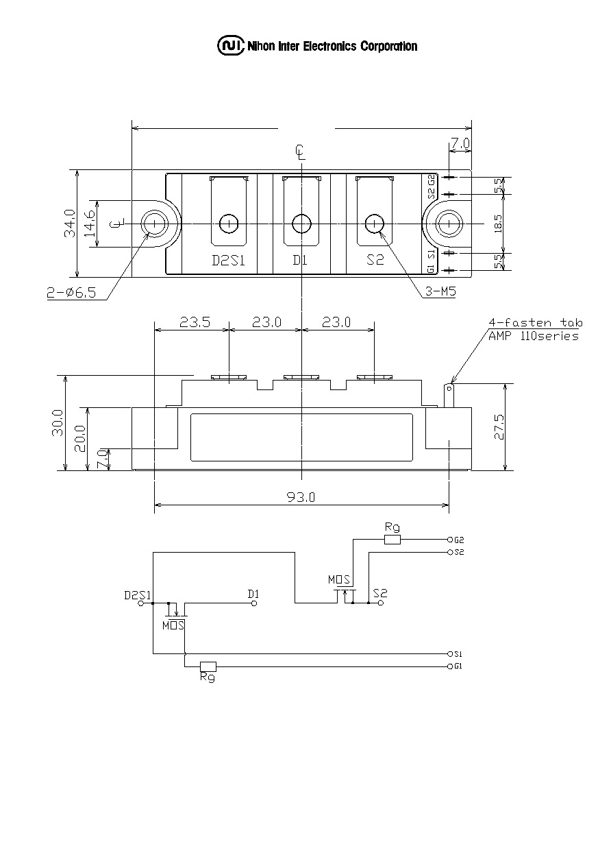
Dimension(mm)
FEATURES
* Dual MOS FETs Cascaded Circuit
* Low On-Resistance and Switching
Dissipation
TYPICAL APPLICATIONS
* Power Supply for the Communications and
the Induction Heating
Approximate Weight : 220g
OUTLINE DRAWING
Circuit
108.0
PD10M440L/441L, P2H10M440L/441L
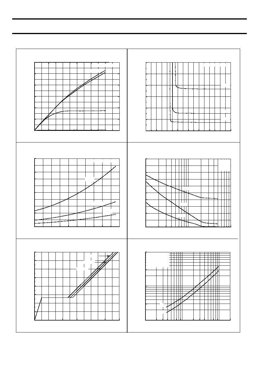
.
0
2
4
6
8
10
12
0
20
40
60
80
100
120
Drain to Source Voltage V
DS
(V)
D
r
a
i
nCur
r
ent
I
D
(A
)
Fig.1- Output Characteristics
(Typical)
T
C
=25
V
GE
=10V
250s PULSE TEST
6V
5V
4V
0
2
4
6
8
10
12
14
16
0
2
4
6
8
10
12
Gate to Source Voltage V
GS
(V)
D
r
a
i
n
t
o
S
o
ur
ce V
o
l
t
a
g
e
V
DS
(V
)
Fig.2- Drain to Source On Voltage
vs. Gate to Source Voltage
(Typical)
T
C
=25
I
D
=40A
I
D
=85A
250s PULSE TEST
I
D
=20A
1
3
10
30
100
0
6
12
18
24
30
Drain to Source Voltage V
DS
(V)
Ca
p
a
ci
t
a
nce C
(n
F
)
Fig.4- Capacitance vs. Drain to Source Voltage
(Typical)
Ciss
Coss
V
GS
=0V
f=1MH
Z
T
C
=25
Crss
0
100
200
300
400
500
600
0
2
4
6
8
10
12
14
16
Total Gate Charge Qg
(nC)
G
a
t
e
t
o
S
o
ur
c
e
V
o
l
t
a
g
e
V
GS
(V
)
Fig.5- Gate Charge vs. Gate to Source Voltage
(Typical)
V
DD
=400V
I
D
=50A
V
DD
=250V
V
DD
=100V
1
2
5
10
20
50
100
200
0.1
0.3
1
3
10
Series Gate Impedance R
G
()
Sw
i
t
chi
ng
T
i
m
e
t
(
s)
Fig.6- Series Gate Impedance vs. Switching Time
(Typical)
V
DD
=250V
I
D
=40A
T
C
=25
80s Pulse Test
ton
toff
-40
0
40
80
120
160
0
4
8
12
16
20
Junction Temperature Tj
()
Dr
a
i
n
t
o
S
o
u
r
ce
Vo
l
t
a
g
e V
DS
(V
)
Fig.3- Drain to Source On Voltage
vs. Junction Temperature
(Typical)
V
GS
=10V
I
D
=20A
I
D
=40A
I
D
=85A
250s PULSE TEST
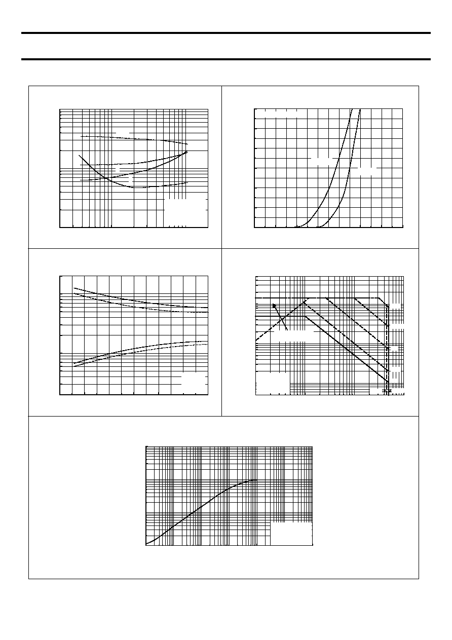
PD10M440L/441L,P2H10M440L/441L
.
.
.
3
10
30
100
200
2
10
30
100
300
1000
Drain Current I
D
(A)
Sw
i
t
chi
ng
T
i
m
e
t
(
s)
Fig.7- Drain Current vs. Switching Time
(Typical)
td(off)
tf
t
r
td(on)
V
DD
=250V
R
G
=7
T
C
=25
80s Pulse Test
0
0.2
0.4
0.6
0.8
1
1.2
1.4
0
20
40
60
80
100
120
Source to Drain Voltage V
SD
(V)
S
o
ur
ce Cur
r
ent
I
S
(A
)
Fig.8- Source to Drain Diode
Forward
Characteristics
(Typical)
T
J
=125
T
J
=25
250s PULSE TEST
0
100
200
300
400
500
600
20
50
100
200
500
1000
2000
-dis/dt
(A/s)
P
e
a
k
R
e
v
e
r
s
e
R
eco
v
e
r
y
Cur
r
ent
I
Rr
M
(A
)
R
e
v
e
r
s
e
R
eco
v
e
r
y
T
i
m
e
t
r
r
(n
s
)
Fig.9- Reverse Recovery Characteristics
(Typical)
I
RrM
trr
...I
S
=40A
I
S
=70A
T
J
=150
1
3
10
30
100
300
1000
0.5
1
2
5
10
20
50
100
200
500
Drain to Source Voltage V
DS
(V)
D
r
a
i
n
C
u
r
r
ent
I
D
(A
)
Fig.10- Maximum Safe Operating Area
T
C=
25
Tj=150MAX
Single Pulse
10s
100s
Operation in this area
is limited by R
DS(on)
1ms
DC
10ms
440L
441L
10
-5
10
-4
10
-3
10
-2
10
-1
1
10
1
1x10
-2
3x10
-2
1x10
-1
3x10
-1
1
3
1x10
1
PULSE DURATION t
(s)
N
o
r
m
al
i
z
e
d
T
r
an
s
i
e
n
t
T
herm
a
l
I
m
ped
a
n
ce
[
rt
h
(J
-
C
)/
Rt
h
(J
-
C
)
]
Fig.11- Normalized Transient Thermal Impedance
(MOSFET)
Per Unit Base
R
th(j-c)
= 0.25/W
1 Shot Pulse