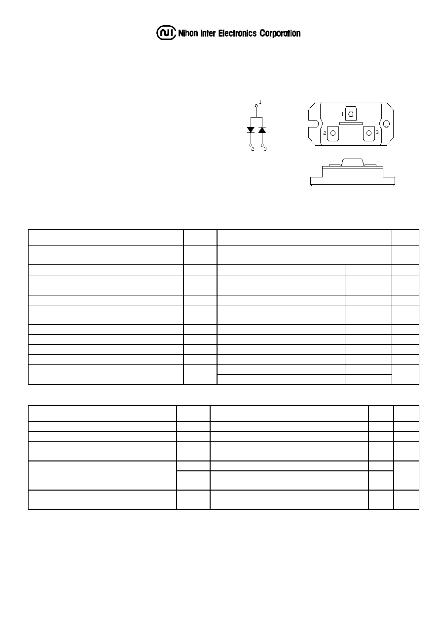
FRD MODULE
50A/500V/trr:90nsec
PD50F5
PD50F5
PD50F5
PD50F5
Maximum Ratings
Approx Net Weight:105g
Voltage
Voltage
Voltage
Voltage Rating
Rating
Rating
Rating
Symbol
PD50F5
Unit
Repetitive Peak Reverse Voltage
per Arm
V
RRM
500 V
Electri
Electri
Electri
Electrical Rating
cal Rating
cal Rating
cal Rating
Condition
Condition
Condition
Condition Rating
Rating
Rating
Rating
Average Rectified Output Current
I
O
50Hz Half Sine Wave condition
per Arm Tc=90
∞
C
50 A
RMS Forward Current
I
F(RMS)
per Arm
78
A
Surge Forward Current
I
FSM
50 Hz Half Sine Wave,1cycle
Non-repetitive per Arm
800 A
I Squared t
I
2
t
2 msec to 10 msec per Arm
3200
A
2
s
Operating JunctionTemperature Range
Tjw
-40 to +150
∞
C
Storage Temperature Range
Tstg
-40 to +125
∞
C
Isoration Voltage
Viso Base Plate to Terminal, AC1min
2000
V
Case mounting(recommended)
2.6
Mounting torque
Ftor
Terminal Screw(recommended)
1.4
N
∑
m
Electrical
∑
Thermal Characteristics
Characteristics
Symbol
Test Conditions
Max. Unit
Peak Forward Voltage
V
FM
I
FM
= 50A, Tj=25
∞
C, per Arm
1.35 V
Peak Reverse Current
I
RM
V
RM
= V
RRM,
Tj= 150
∞
C, per Arm
10 mA
Reverse Recovery Time
trr I
FM
= 10A, -di/dt= 50 A/
µ
s, Ta= 25
∞
C
Per Arm
90 ns
Rth(j-c) Junction to Case per Arm
0.8
Thermal Resistance
Rth(c-f)
Base Plate to Heat Sink with Thermal
Compound
0.1
∞
C/W
Internal Lead Inductance
Ls
Anode Terminal to Cathode Terminal
Per Element
30 nH
FEATURES
* Isolated Base
* Dual Diode Doubler Circuit
* Ultra Fast Recovery
* High Surge Capability
* UL Recognized, File No. E187184
TYPICAL APPLICATIONS
* High Frequency Rectification
OUTLINE DRAWING
