
- 1 -
NJG1107HB3
LOW NOISE AMPLIFIER GaAs MMIC
n
GENERAL DESCRIPTION
n
PACKAGE OUTLINE
NJG1107HB3 is a Low Noise Amplifier GaAs MMIC
designed for GPS This amplifier provides low noise figure,
high gain and high IP3 operated by single low positive power
supply.
This amplifier
includes internal self-bias circuit and input
DC blocking capacitor.
This amplifier can be tuned to wide frequency point
(1.5GHz~2.4GHz).
An ultra small and ultra thin package of
USB8-B3 is
adopted.
n
FEATURES
l
Low voltage operation
+2.7V typ.
l
Low current consumption
2.5mA typ.
l
High small signal gain
17dB typ. @f=1.575GHz
l
Low noise figure
1.1dB typ. @f=1.575GHz
l
High Input IP3
-4.0dBm typ. @f=1.575+1.5751GHz
l
Ultra small & ultra thin package
USB8-B3 (Mount Size: 1.5x1.5x0.75mm)
n
PIN CONFIGURATION
Note: Specifications and description listed in this catalog are subject to change without prior notice.
NJG1107HB3
HB3 Type
(Top View)
Pin Connection
1.RF
OUT
2.N/C
3.EXTCAP
4.N/C
5.N/C
6.GND
7. RF
IN
8. N/C
Orientation Mark
A
MP
1
2
3
7
6
5
4
8

NJG1107HB3
- 2 -
n
ABSOLUTE MAXIMUM RATINGS
(T
a
=+25�C, Z
s
=Z
l
=50
)
PARAMETER
SYMBOL
CONDITIONS
RATINGS
UNIT
Drain Voltage
V
DD
6.0
V
Input Power
Pin
V
DD
=2.7V
+15
dBm
Power Dissipation
P
D
At on PCB board
135
mW
Operating Temp.
T
opr
-40~+85
�C
Storage Temp.
T
stg
-55~+150
�C
n
ELECTRICAL CHARACTERISTICS
(V
DD
=2.7V, f=1.575GHz, T
a
=+25�C, Z
s
=Z
l
=50
, TEST CIRCUIT)
PARAMETER
SYMBOL
CONDITIONS
MIN
TYP
MAX
UNIT
Operating Frequency
freq1
1.57
1.575
1.58
GHz
Drain Voltage
V
DD
2.5
2.7
5.5
V
Operating Current
I
DD
RF OFF
-
2.5
3.2
mA
Small Signal Gain
Gain
15.0
17.0
-
dB
Noise Figure
NF
-
1.1
1.3
dB
Pin at 1dB Gain
Compression point
P
-1dB
-20.0
-16.0
-
dBm
Input 3rd Order
Intercept Point
IIP3
f=1.575+1.5751GHz
RFin=-35dBm
-6.0
-4.0
-
dBm
RF Input Port
VSWR
VSWR
i
-
1.6
2.0
RF Output Port
VSWR
VSWR
o
1.6
2.0

NJG1107HB3
- 3 -
n
PIN CONFIGURATION
Pin
Function
Description
1
Rfout
RF output and voltage supply pin. External matching circuits and a bypass
capacitor is required. L3 is a RF choke inductor and C1 is a DC blocking capacitor.
These elements are used as output matching circuit. C2 is a bypass capacitor.
2,4,5,8 N/C
Neutral terminal. Should be connected to the ground.
3
EXTCAP An external bypass capacitor is required.
6
GND
Ground pin. To keep good RF grounding performance, please use multiple via
holes to connect with ground plane and this pin.
7
Rfin
RF input pin. A DC blocking capacitor is not required. An external matching circuit
is required.
NJG1107HB3
- 4 -
n
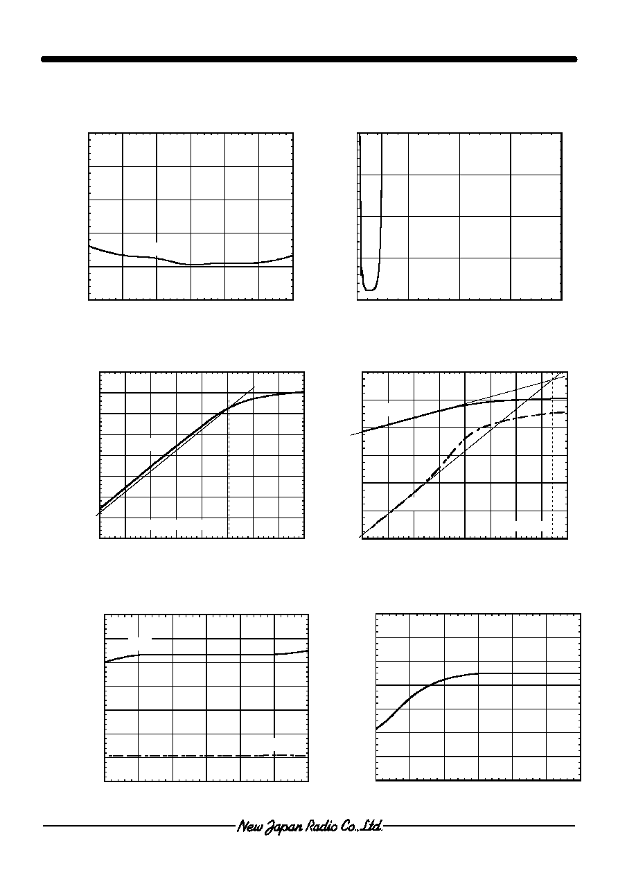
TYPICAL CHARACTERISTICS
0
1
2
3
4
5
1400
1450
1500
1550
1600
1650
1700
NF vs. frequency
NF (dB)
frequency (MHz)
NF
(V
DD
=2.7V, Ta=25
o
C)
-30
-25
-20
-15
-10
-5
0
5
10
-40
-35
-30
-25
-20
-15
-10
-5
0
Pout vs. Pin
Pout (dBm)
Pin (dBm)
Pout
P-1dB(IN)=-14.8dBm
(V
D D
=2.7V, f=1575MHz, Ta=25
o
C)
-100
-80
-60
-40
-20
0
20
-40
-35
-30
-25
-20
-15
-10
-5
0
Pout, IM3 vs. Pin
Pout, IM3 (dBm)
Pin (dBm)
Pout
IM3
IIP3=-2.8dBm
(V
DD
=2.7V, f1=1575MHz, f2=f1+100kHz, Ta=25
o
C)
0
5
10
15
20
0
5
10
15
20
k factor vs. frequency
k factor
frequency (GHz)
(V
DD
=2.7V, Ta=25
o
C)
12
13
14
15
16
17
18
19
0
1
2
3
4
5
6
7
2.5
3
3.5
4
4.5
5
5.5
Gain, NF vs. V
DD
Gain (dB)
NF (dB)
V
DD
(V)
(f=1575MHz, Ta=25
o
C)
Gain
NF
-20
-18
-16
-14
-12
-10
-8
-6
2.5
3
3.5
4
4.5
5
5.5
P-1dB(IN) vs. V
DD
P-1dB(IN) (dBm)
V
DD
(V)
(f=1575MHz, Ta=25
o
C)

- 5 -
NJG1107HB3
n
TYPICAL CHARACTERISTICS
11
12
13
14
15
16
17
18
19
0
0.5
1
1.5
2
2.5
3
3.5
4
-50
0
50
100
Gain, NF vs. Temperature
Gain (dB)
NF (dB)
Temperature (
o
C)
(V
DD
=2.7V, f=1575MHz)
Gain
NF
-19
-18
-17
-16
-15
-14
-13
-12
-11
-50
0
50
100
P-1dB(IN) vs. Temperature
P-1dB(IN) (dBm)
Temperature (
o
C)
(V
DD
=2.7V, f=1575MHz)
8
9
10
11
12
13
14
15
16
-5
-4
-3
-2
-1
0
1
2
3
-50
0
50
100
OIP3, IIP3 vs. Temperature
OIP3 (dBm)
IIP3 (dBm)
Temperature (
o
C)
(V
DD
=2.7V, f1=1575MHz, f2=f1+100kHz, Pin=-35dBm)
OIP3
IIP3
0
1
2
3
4
5
-50
0
50
100
I
DD
vs. Temperature
I
DD
(mA)
Temperature (
o
C)
(V
DD
=2.7V, RF=OFF)