NJG1542HB3
- 1 -
SPDT SWITCH GaAs MMIC
n
GENERAL DESCRIPTION
n
PACKAGE OUTLINE
NJG1542HB3 is a GaAs SPDT switch IC that features
small-sized package and low insertion loss , and ideally
suited for T/R switch of digital cordless telephone or other
digital wireless systems.
This switch is operated in the wide frequency range from
100MHz to 2.5GHz at low operating voltage from +2.5V.
The ultra small & ultra thin USB8-B3 package is adopted.
n
FEATURES
l
Low insertion loss
0.4dB typ. @f=1.0GHz
0.45dB typ. @f=2.0GHz
0.5dB typ. @f=2.5GHz
l
High isolation
25dB typ. @f=1.0GHz
20dB typ. @f=2.0GHz
18dB typ. @f=2.5GHz
l
Pin at 1dB compression point
27dBm typ. @f=2.5GHz
l
Low control current
5uA typ.
l
Ultra small & ultra thin package
USB8-B3 (Package size: 1.5x1.5x0.75mm)
n
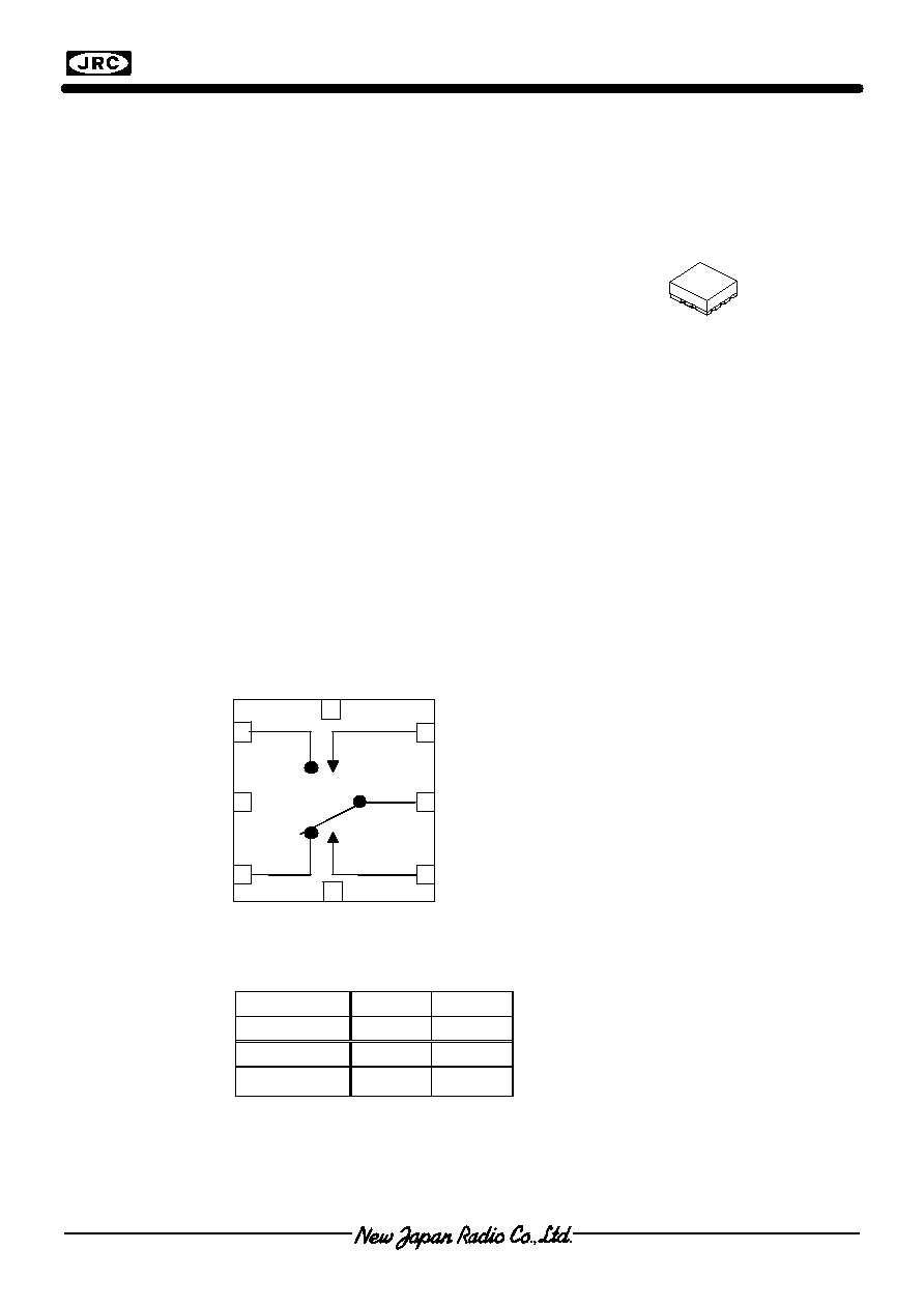
PIN CONFIGURATION
n
TRUTH TABLE
Note: Reversed logic version of this device is NJG1600HB3
.
VCTL1
H
L
VCTL2
L
H
PC-P1
ON
OFF
PC-P2
OFF
ON
"H"=V
CTL (H)
, "L"=V
CTL (L)
Pin connection
1.P1
2.GND
3.P2
4.GND
5.VCTL2
6.PC
7.VCTL1
8.GND
USB8-B3 Type
(TOP VIEW)
NJG1542HB3
5
6
7
3
2
1
8
4

NJG1542HB3
- 2 -
n
ABSOLUTE MAXIMUM RATINGS
PARAMETER
SYMBOL
CONDITIONS
CONDITIONS
UNITS
RF Input Power
P
IN
V
CTL
=0V/3V
29
dBm
Control Voltage
V
CTL
VCTL terminal
7.5
V
Operating Temp.
T
opr
-40~+85
�C
Storage Temp.
T
stg
-55~+150
�C
n
ELECTRICAL CHARACTERISTICS
(General conditions: V
CTL (L)
=0V, V
CTL (H)
=3V, Z
S
=Z
l
=50
, T
a
=25�C)
PARAMETERS
SYMBOL
CONDITIONS
MIN
TYP
MAX
UNITS
Control Voltage (LOW)
V
CTL (L)
-0.2
-
0.2
V
Control Voltage (HIGH)
V
CTL (H)
2.5
3.0
6.5
V
Control Current
I
CTL
f=2.5GHz, P
IN
=18dBm
-
5
10
uA
Insertion Loss 1
LOSS1 f=1.0GHz, P
IN
=18dBm
-
0.4
0.55
dB
Insertion Loss 2
LOSS2 f=2.0GHz, P
IN
=18dBm
-
0.45
0.6
dB
Insertion Loss 3
LOSS3 f=2.5GHz, P
IN
=18dBm
-
0.5
0.65
dB
Isolation 1
ISL1
f=1.0GHz, P
IN
=18dBm
22
25
-
dB
Isolation 2
ISL2
f=2.0GHz, P
IN
=18dBm
17
20
-
dB
Isolation 3
ISL2
f=2.5GHz, P
IN
=18dBm
15
18
-
dB
Pin at 1dB
Compression Point 1
P
-1dB
(1) f=2.5GHz(V=0V/2.7V)
24.5
26
-
dBm
Pin at 1dB
Compression Point 2
P
-1dB
(2) f=2.5GHz
25
27
-
dBm
VSWR
VSWR
f=0.1~2.5GHz, ON state
-
1.2
1.4
Switching time
T
SW
f=0.1~2.5GHz
-
20
100
ns

NJG1542HB3
- 3 -
n
TERMINAL INFORMATION
No.
SYMBOL
DESCRIPTION
1
P1
RF port. This port is connected with PC port by controlling 7
th
pin (V
CTL(H)
)
to 2.5~6.5V and 5
th
pin(V
CTL(L)
) to -0.2~+0.2V. An external capacitor is
required to block the DC bias voltage of internal circuit. (100MHz: 0.01uF,
0.1~0.5GHz: 1000pF, 0.5~2.5GHz: 56pF)
2
GND
Ground terminal. Please connect this terminal with ground plane as close
as possible for excellent RF performance.
3
P2
RF port. This port is connected with PC port by controlling 5
th
pin (V
CTL (H)
)
to 2.5~6.5V and 7
th
pin(V
CTL(L)
) to -0.2~+0.2V. An external capacitor is
required to block the DC bias voltage of internal circuit. (100MHz: 0.01uF,
0.1~0.5GHz: 1000pF, 0.5~2.5GHz: 56pF)
4
GND
Ground terminal. Please connect this terminal with ground plane as close
as possible for excellent RF performance.
5
VCTL2
Control port 2. The voltage of this port controls PC to P2 state. The `ON'
and `OFF' state is toggled by controlling voltage of this terminal such as
high-state (2.5~6.5V) or low-state (-0.2~+0.2V). The voltage of 7
th
pin have
to be set to opposite state. The bypass capacitor has to be chosen to
reduce switching time delay from 10pF~1000pF range.
6
PC
Common RF port. In order to block the DC bias voltage of internal circuit,
an external capacitor is required. (100MHz:0.01uF, 0.1~0.5GHz: 1000pF,
0.5~2.5GHz: 56pF)
7
VCTL1
Control port 1. The voltage of this port controls PC to P1 state. The `ON'
and `OFF' state is toggled by controlling voltage of this terminal such as
high-state (2.5~6.5V) or low-state (-0.2~+0.2V). The voltage of 5
th
pin have
to be set to opposite state. The bypass capacitor has to be chosen to
reduce switching time delay from 10pF~1000pF range.
8
GND
Ground terminal. Please connect this terminal with ground plane as close
as possible for excellent RF performance.
NJG1542HB3
- 4 -
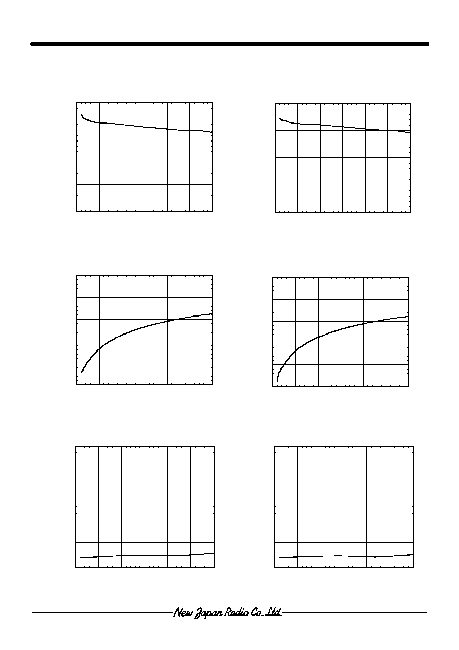
1.0
1.2
1.4
1.6
1.8
2.0
0.0
0.5
1.0
1.5
2.0
2.5
3.0
PC-P1 VSWR vs. Frequency
VSWR
Frequency (GHz)
(VCTL=3.0V/0V,P1 port)
1.0
1.2
1.4
1.6
1.8
2.0
0.0
0.5
1.0
1.5
2.0
2.5
3.0
PC-P2 VSWR vs. Frequency
VSWR
Frequency (GHz)
(VCTL=3.0V/0V,P2 port)
-2.0
-1.5
-1.0
-0.5
0.0
0.0
0.5
1.0
1.5
2.0
2.5
3.0
(PC-P1 ON, VCTL=3.0V/0V, Pin=-10dBm)
Insertion Loss (dB)
Frequency (GHz)
PC-P1 Insertion Loss vs. Frequency
-50
-40
-30
-20
-10
0
0.0
0.5
1.0
1.5
2.0
2.5
3.0
(PC-P2 ON, VCTL=3.0V/0V, Pin=-10dBm)
Isolation (dB)
Frequency (GHz)
PC-P1 Isolation vs. Frequency
n
ELECTRICAL CHARACTERISTICS
(0.1~3.0GHz,
with application circuit, without DC Blocking Capacitor, Losses of external circuit are excluded)
-2.0
-1.5
-1.0
-0.5
0.0
0.0
0.5
1.0
1.5
2.0
2.5
3.0
(PC-P2 ON, VCTL=3.0V/0V, Pin=-10dBm)
Insertion Loss (dB)
Frequency (GHz)
PC-P2 Insertion Loss vs. Frequency
-50
-40
-30
-20
-10
0
0.0
0.5
1.0
1.5
2.0
2.5
3.0
(PC-P1 ON, VCTL=3.0V/0V, Pin=-10dBm)
Isolation (dB)
Frequency (GHz)
PC-P2 Isolation vs. Frequency

NJG1542HB3
- 5 -
-2.0
-1.5
-1.0
-0.5
0.0
12
14
16
18
20
22
24
26
28
30
(PC-P1 ON, f=2.5GHz)
VCTL=2.5V
VCTL=2.7V
VCTL=3.0V
VCTL=5.0V
VCTL=6.5V
Insertion Loss (dB)
Input Power (dBm)
PC-P1 Insertion Loss vs. Input Power
10
15
20
25
30
0
10
20
30
40
12
14
16
18
20
22
24
26
28
30
(PC-P1 ON, f=2.5GHz)
VCTL=2.5V
VCTL=2.7V
VCTL=3.0V
VCTL=5.0V
VCTL=6.5V
Output Power (dBm)
ICTL (uA)
Input Power (dBm)
PC-P1 Output Power, ICTL vs. Input Power
-0.8
-0.7
-0.6
-0.5
-0.4
-0.3
-0.2
-50
0
50
100
(PC-P1 ON, f=2.5GHz, Pin=18dBm)
VCTL=2.5V
VCTL=2.7V
VCTL=3.0V
VCTL=5.0V
VCTL=6.5V
Insertion Loss (dB)
Ambient Temperature (
o
C)
PC-P1 Insertion Loss vs. Ambient Temperature
0
5
10
15
20
-50
0
50
100
(PC-P1 ON, f=2.5GHz, Pin=18dBm)
VCTL=2.5V
VCTL=2.7V
VCTL=3.0V
VCTL=5.0V
VCTL=6.5V
ICTL (uA)
Ambient Temperature (
o
C)
ICTL vs. Ambient Temperature
20
22
24
26
28
30
-50
0
50
100
(PC-P1 ON, f=2.5GHz)
VCTL=2.5V
VCTL=2.7V
VCTL=3.0V
P-1dB (dBm)
Ambient Temperature (
o
C)
PC-P1 P-1dB vs. Ambient Temperature
n
ELECTRICAL CHARACTERISTICS
(Application circuit (Parts list 2))
-25
-20
-15
-10
-50
0
50
100
(PC-P1 ON, VCTL=3.0V/0V, f=2.5GHz, Pin=18dBm)
Isolation (dB)
Ambient Temperature (
o
C)
PC-P2 Isolation vs. Ambient Temperature