 | –≠–ª–µ–∫—Ç—Ä–æ–Ω–Ω—ã–π –∫–æ–º–ø–æ–Ω–µ–Ω—Ç: NJM2822 | –°–∫–∞—á–∞—Ç—å:  PDF PDF  ZIP ZIP |
NJM2820, NJM2821, NJM2822
Ver 2.1
- 1 -
ADJUSTABLE HIGH PRECISION SHUNT REGULATOR
GENERAL DESCRIPTION
PACKAGE OUTLINE
FEATURES
High Precision Voltage Reference
1.250V±0.7%
Flow Soldering*
Minimum Input Current
80uA typ.
Operating Voltage
V
REF
to 13V
Adjustable Output Voltage For External Resistance two Parts
Bipolar Technology
Package Outline MTP5
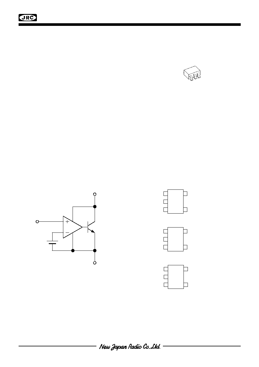
BLOCK
DIAGRAM
PIN CONFIGURATION
* These contents are based on the result that evaluated the arbitrary sample. The characteristic is not guaranteed. The design and
reliability that fully considered flow mounting are checked but the influence by temperature profile etc. is also considered. Please consult
with sales representatives for a recommendation temperature profile.
The
NJM2820
/
2821
/
2822
is a 1.25V precision shunt
regulator.
High precision voltage accuracy of ±0.7%* is realized by
the total optimization from chip design to packaging. In
addition, it features low cathode current of 80uA for low
current operation.
It is suitable for AC-DC converter secondary circuit,
reference voltage applications for A/D and D/A converters,
and other applications where precision reference is required.
NJM2820F
NJM2821F
NJM2822F
ANODE
REFERENCE
V
REF
CATHODE
NJM2820F
NJM2821F
CATHODE
ANODE
REFERENCE
NC
1
2
3
5
4
NC
CATHODE
ANODE
REFERENCE
NC
1
2
3
5
4
NC
NJM2822F
REFERENCE
CATHODE
ANODE
1
2
3
5
4
NC ANODE
NJM2820, NJM2821, NJM2822
- 2 -
ABSOLUTE MAXIMUM RATINGS (Ta=25∞C)
PARAMETER SYMBOL
MAXIMUM
RATINGS
UNIT
Cathode Voltage
V
KA
14 V
Continuous Cathode Current
I
K
-30
50
mA
Reference Input Current
I
REF
-10
0.05
mA
Power Dissipation
P
D
(MTP5) 200
mW
Operating Temperature Range
T
OPR
-40
+85
∞C
Storage Temperature Range
T
STG
-40
+150
∞C
RECOMMENDED OPERATING CONDITIONS (Ta=25∞C)
PARAMETER SYMBOL
MIN.
TYP.
MAX.
UNIT
Cathode Voltage
V
KA
V
REF
≠
13 V
Cathode Current
I
K
0.5 ≠
30 mA
ELECTRICAL CHARACTERISTICS (I
K
=1mA,Ta=25∞C)
PARAMETER SYMBOL
TEST
CONDITION
MIN.
TYP.
MAX.
UNIT
Reference Voltage
V
REF
V
KA
=V
REF
(*1)
1241 1250 1259
mV
V
REF
V
KA
5V
(*2)
≠ ≠
±
2.7
mV/V
Reference Voltage
Change vs. Cathode
Voltage Change
V
REF
/
V
KA
5V
V
KA
13V
(*2)
≠ ≠
±
2.0
mV/V
Reference Input Current
I
REF
R1=10k, R2=
(*2)
≠ 2.0
4.0
uA
Minimum Input Current
I
MIN
V
KA
=V
REF
, V
REF
=1% (*1)
≠ 80
500
uA
Cathode Current
(Off Cond.)
I
OFF
V
KA
=13V, V
REF
=0V
(*3)
≠ 0.01
1.0
uA
Dynamic Impedance
Z
KA
V
KA
= V
REF
, f
1kHz
0.5mA
I
K
30mA
(*1) ≠
0.12
≠
TEMPERATURE CHARACTERISTICS (I
K
=1mA,Ta=-40∞C
85∞C)
PARAMETER SYMBOL
TEST
CONDITION
MIN.
TYP.
MAX.
UNIT
Reference Voltage
Change
V
REF
V
KA
=V
REF
(*1)
≠ ±10 ≠
mV
Reference Input Current
Change
I
REF
R1=10k,R2= (*2)
≠ 0.5 ≠ uA
V
REF
∑∑∑Reference voltage includes error.
(*1): Test Circuit (Fig.1)
(*2): Test Circuit (Fig.2)
(*3): Test Circuit (Fig.3)
In case of NJM2822, all electrical characteristics are measured referencing to the anode terminal of PIN 5.

NJM2820, NJM2821, NJM2822
- 3 -
TEST CIRCUIT
Fig.1 V
KA
=V
REF
to test circuit
Fig.2 V
KA
>V
REF
to test circuit
V
O
=V
KA
=V
REF
1
R
I
2
R
1
R
1
V
V
V
REF
REF
KA
O
◊
+
+
=
=
Fig.3 I
OFF
to test circuit
Fig.4 Gain and Phase to test circuit
POWER DISSIPATION VS. AMBIENT TEMPERATURE
0
50
100
150
200
250
0
25
50
75
100
Ambient Temperature Ta (∞C)
Power Dissipat
ion P
D
(mW)
INPUT
V
KA
I
K
V
REF
I
K
=1mA
10k
10k
470uF
INPUT
V
KA
I
K
V
REF
I
REF
R1
R2
INPUT
V
KA
I
OFF

NJM2820, NJM2821, NJM2822
- 4 -
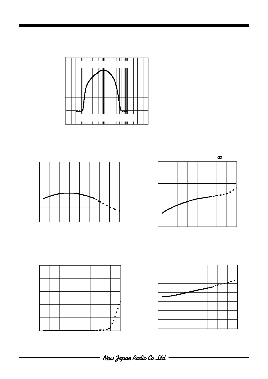
TYPICAL CHARACTERISTICS
Dynamic Impedance
(I
K
=0.5~30mA,V
KA
=V
REF
,Ta=25∞C)
0
0.2
0.4
0.6
0.8
1
1.2
1
10
100
1k
10k
100k
Cathode Current Frequency f (Hz)
Dynamic I
m
pedance |Z
KA
| (
)
Reference Voltage vs. Cathode Current
(V
KA
=V
REF
,Ta=25∞C)
1240
1245
1250
1255
1260
0
10
20
30
Cathode Current I
K
(mA)
Refer
enc
e Voltage
V
REF
(
m
V)
Reference Voltage vs. Cathode Current
(V
KA
=V
REF
,Ta=25∞C)
600
800
1000
1200
1400
0
20
40
60
80
100
Cathode Current I
K
(uA)
Ref
e
rence Volt
age V
REF
(m
V)
Reference Voltage Change vs. Cathode Voltage
(I
K
=1mA,R1=Variable,R2=10k,Ta=25∞C)
0
1
2
3
4
0
5
10
15
Cathode Voltage V
KA
(V)
Refer
ence Voltage Change
V
REF
(
m
V)
Cathode Current (Off Cond.) vs. Cathode Voltage
(V
REF
=0V,Ta=25∞C)
0
0.2
0.4
0.6
0.8
1
0
5
10
15
Cathode Voltage V
KA
(V)
Cat
hode Current
I
OF
F
(n
A)
Voltage Gain ∑ Phase vs. Frequency
(Fig.4 Test Circuit,Ta=25∞C)
-80
-60
-40
-20
0
20
40
60
80
100
1k
10k
100k
1M
10M
Frequency f (Hz)
Volt
age G
a
in
A
V
(d
B)
-360
-270
-180
-90
0
90
180
270
360
Phase
(deg)
Gain
Phase
NJM2820, NJM2821, NJM2822
- 5 -
TYPICAL CHARACTERISTICS
Sefty Operating Boundary Condition
(V
KA
=V
REF
,Ta=25∞C)
0
50
100
150
200
250
0.001
0.01
0.1
1
10
Output Capacetance Co (uF)
Cat
hode Current
I
K
(u
A)
Stable Operaion Region
Aunstable Operaion Region
Reference Input Current vs. Temperature
(I
K
=1mA,R1=10k,R2= )
1.5
2
2.5
3
-50 -25
0
25 50 75 100 125 150
Ambient Temperature Ta (∞C)
Ref
e
rence I
nput
Current
I
REF
(u
A)
Reference Voltage vs. Temperature
(I
K
=1mA,V
KA
=V
REF
)
1240
1245
1250
1255
1260
-50 -25
0
25
50 75 100 125 150
Ambient Temperature Ta (∞C)
Ref
e
rence Volt
age V
REF
(mV)
Cathode Current (Off Cond.) vs. Temperature
(V
KA
=13V,V
REF
=0V)
0
0.2
0.4
0.6
0.8
1
-50 -25
0
25 50
75 100 125 150
Ambient emperature Ta (∞C)
Cat
hode Current
I
OF
F
(uA)
Output Noise Voltage vs. Temperature
(I
K
=1mA,V
KA
=V
REF
)
0
20
40
60
80
100
120
140
-50 -25
0
25 50 75 100 125 150
Ambient Temperature Ta (∞C)
O
u
tput Noise Voltage
V
NO
(u
V
r
m
s
)
Note) Oscillation might occur while operating within
the range of safety curve.
So that, it is necessary to make ample
margins by taking considerations of fluctuation
of the device.

NJM2820, NJM2821, NJM2822
- 6 -
MEMO
[CAUTION]
The specifications on this databook are only
given for information , without any guarantee
as regards either mistakes or omissions. The
application circuits in this databook are
described only to show representative usages
of the product and not intended for the
guarantee or permission of any right including
the industrial rights.