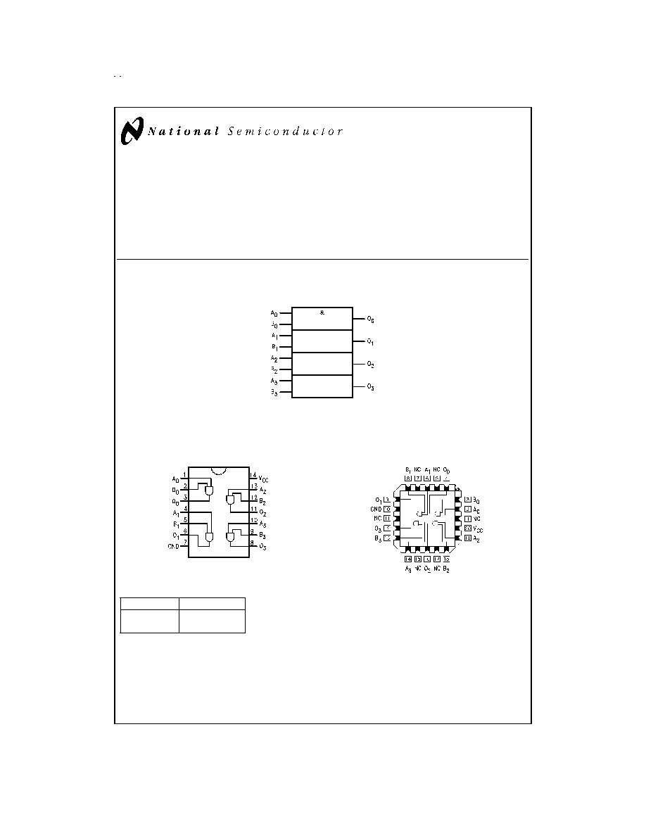
54AC08
Quad 2-Input AND Gate
General Description
The 'AC08 contains four, 2-input AND gates.
Features
n
I
CC
reduced by 50%
n
Outputs source/sink 24 mA
n
Standard Microcircuit Drawing (SMD) 5962-87615
n
For Military 54ACT08 device, see 54ACTQ08
Logic Symbols
Connection Diagrams
Pin Names
Description
A
n
, B
n
Inputs
O
n
Outputs
FACT
TM
is a trademark of Fairchild Semiconductor Corporation.
IEEE/IEC
DS100260-1
Pin Assignment
for DIP and Flatpak
DS100260-3
Pin Assignment
for LCC
DS100260-2
September 1998
54AC08
Quad
2-Input
AND
Gate
© 1998 National Semiconductor Corporation
DS100260
www.national.com
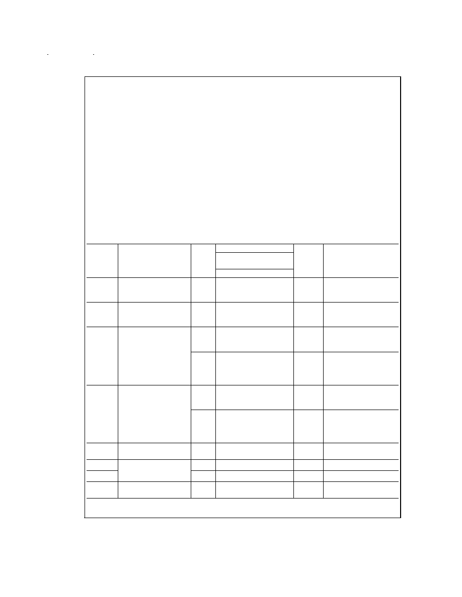
Absolute Maximum Ratings
(Note 1)
If Military/Aerospace specified devices are required,
please contact the National Semiconductor Sales Office/
Distributors for availability and specifications.
Supply Voltage (V
CC
)
-0.5V to +7.0V
DC Input Diode Current (I
IK
)
V
I
= -0.5V
-20 mA
V
I
= V
CC
+ 0.5V
+20 mA
DC Input Voltage (V
I
)
-0.5V to V
CC
+ 0.5V
DC Output Diode Current (I
OK
)
V
O
= -0.5V
-20 mA
V
O
= V
CC
+ 0.5V
+20 mA
DC Output Voltage (V
O
)
-0.5V to V
CC
+ 0.5V
DC Output Source
or Sink Current (I
O
)
±
50 mA
DC V
CC
or Ground Current
per Output Pin (I
CC
or I
GND
)
±
50 mA
Storage Temperature (T
STG
)
-65∞C to +150∞C
Junction Temperature (T
J
)
CDIP
175∞C
Recommended Operating
Conditions
Supply Voltage (V
CC
)
'AC
2.0V to 6.0V
Input Voltage (V
I
)
0V to V
CC
Output Voltage (V
O
)
0V to V
CC
Operating Temperature (T
A
)
54AC
-55∞C to +125∞C
Minimum Input Edge Rate (
V/
t)
'AC Devices
V
IN
from 30% to 70% of V
CC
V
CC
@
3.3V, 4.5V, 5.5V
125 mV/ns
Note 1: Absolute maximum ratings are those values beyond which damage
to the device may occur. The databook specifications should be met, without
exception, to ensure that the system design is reliable over its power supply,
temperature, and output/input loading variables. National does not recom-
mend operation of FACT
TM
circuits outside databook specifications.
DC Characteristics for 'AC Family Devices
54AC
Symbol
Parameter
V
CC
T
A
= -55∞C to +125∞C
Units
Conditions
(V)
Guaranteed Limits
V
IH
Minimum High Level
3.0
2.1
V
OUT
= 0.1V
Input Voltage
4.5
3.15
V
or V
CC
- 0.1V
5.5
3.85
V
IL
Maximum Low Level
3.0
0.9
V
OUT
= 0.1V
Input Voltage
4.5
1.35
V
or V
CC
- 0.1V
5.5
1.65
V
OH
Minimum High Level
3.0
2.9
I
OUT
= -50 µA
Output Voltage
4.5
4.4
V
5.5
5.4
(Note 2) V
IN
= V
IL
or V
IH
3.0
2.4
-12 mA
4.5
3.7
V
I
OH
-24 mA
5.5
4.7
-24 mA
V
OL
Maximum Low Level
3.0
0.1
I
OUT
= 50 µA
Output Voltage
4.5
0.1
V
5.5
0.1
(Note 2) V
IN
= V
IL
or V
IH
3.0
0.5
12 mA
4.5
0.5
V
I
OL
24 mA
5.5
0.5
24 mA
I
IN
Maximum Input
5.5
±
1.0
µA
V
I
= V
CC
, GND
Leakage Current
I
OLD
(Note 3) Minimum
Dynamic Output
Current
5.5
50
mA
V
OLD
= 1.65V Max
I
OHD
5.5
-50
mA
V
OHD
= 3.85V Min
I
CC
Maximum Quiescent
5.5
40.0
µA
V
IN
= V
CC
Supply Current
or GND
Note 2: All outputs loaded; thresholds on input associated with output under test.
Note 3: Maximum test duration 2.0 ms, one output loaded at a time.
www.national.com
2
AC Electrical Characteristics
54AC
V
CC
T
A
= -55∞C
Symbol
Parameter
(V)
to +125∞C
Units
(Note 4)
C
L
= 50 pF
Min
Max
t
PLH
Propagation Delay
3.3
1.0
12.5
ns
5.0
1.0
9.0
t
PHL
Propagation Delay
3.3
1.0
12.5
ns
5.0
1.0
9.0
Note 4: Voltage Range 3.3 is 3.3V
±
0.3V
Voltage Range 5.0 is 5.0V
±
0.5V
Capacitance
Symbol
Parameter
Typ
Units
Conditions
C
IN
Input Capacitance
4.5
pF
V
CC
= OPEN
C
PD
Power Dissipation
20.0
pF
V
CC
= 5.0V
Capacitance
www.national.com
3

Physical Dimensions
inches (millimeters) unless otherwise noted
20-Terminal Ceramic Leadless Chip Carrier (L)
NS Package Number E20A
14-Lead Ceramic Dual-In-Line Package (D)
NS Package Number J14A
www.national.com
5