 | –≠–ª–µ–∫—Ç—Ä–æ–Ω–Ω—ã–π –∫–æ–º–ø–æ–Ω–µ–Ω—Ç: 54AC169 | –°–∫–∞—á–∞—Ç—å:  PDF PDF  ZIP ZIP |

54AC169
∑
54ACT169
4-Stage Synchronous Bidirectional Counter
General Description
The 'AC/'ACT169 is fully synchronous 4-stage up/down
counter. The 'AC/'ACT169 is a modulo-16 binary counter. It
features a preset capability for programmable operation,
carry lookahead for easy cascading and a U/D input to con-
trol the direction of counting. All state changes, whether in
counting
or
parallel
loading,
are
initiated
by
the
LOW-to-HIGH transition of the Clock.
Features
n
I
CC
reduced by 50%
n
Synchronous counting and loading
n
Built-In lookahead carry capability
n
Presettable for programmable operation
n
Outputs source/sink 24 mA
n
'ACT has TTL-compatible inputs
n
Standard Microcircuit Drawing (SMD)
5962-91603
Logic Symbols
Pin
Names
Description
CEP
Count Enable Parallel Input
CET
Count Enable Trickle Input
CP
Clock Pulse Input
P
0
≠P
3
Parallel Data Inputs
PE
Parallel Enable Input
U/D
Up-Down Count Control Input
Q
0
≠Q
3
Flip-Flop Outputs
TC
Terminal Count Output
FACT
TM
is a trademark of Fairchild Semiconductor Corporation.
DS100276-1
IEEE/IEC
DS100276-2
July 1998
54AC169
∑
54ACT169
4-Stage
Synchronous
Bidirectional
Counter
© 1998 National Semiconductor Corporation
DS100276
www.national.com
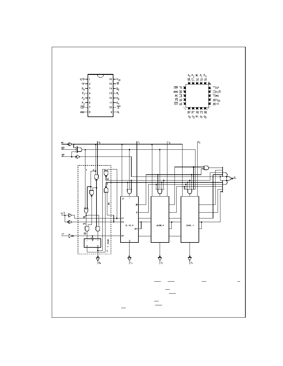
Connection Diagrams
Logic Diagram
Functional Description
The 'AC/'ACT169 uses edge-triggered J-K-type flip-flops
and have no constraints on changing the control or data in-
put signals in either state of the Clock. The only requirement
is that the various inputs attain the desired state at least a
setup time before the rising edge of the clock and remain
valid for the recommended hold time thereafter. The parallel
load operation takes precedence over the other operations,
as indicated in the Mode Select Table. When PE is LOW, the
data on the P
0
≠P
3
inputs enters the flip-flops on the next ris-
ing edge of the Clock. In order for counting to occur, both
CEP and CET must be LOW and PE must be HIGH; the U/D
input then determines the direction of counting. The Terminal
Count (TC) output is normally HIGH and goes LOW, pro-
vided that CET is LOW, when a counter reaches zero in the
Count Down mode or reaches 15 in the Count Up mode. The
TC output state is not a function of the Count Enable Parallel
(CEP) input level. If an illegal state occurs, the 'AC169 will
return to the legitimate sequence within two counts. Since
Pin Assignment
for DIP and Flatpak
DS100276-3
Pin Assignment
for LCC
DS100276-4
DS100276-5
Please note that this diagram is provided only for the understanding of logic operations and should not be used to estimate propagation delays.
www.national.com
2

Functional Description
(Continued)
the TC signal is derived by decoding the flip-flop states,
there exists the possibility of decoding spikes on TC. For this
reason the use of TC as a clock signal is not recommended
(see logic equations below).
1.
Count Enable = CEP
∑CET ∑ PE
2.
Up: TC = Q
0
∑Q
1
∑Q
2
Q
3
∑(Up)∑CET
3.
Down: TC = Q
0
∑ Q
1
∑Q
2
∑Q
3
∑(Down)∑CET
Mode Select Table
PE
CEP
CET
U/D
Action on Rising
Clock Edge
L
X
X
X
Load (P
n
to Q
n
)
H
L
L
H
Count Up (Increment)
H
L
L
L
Count Down (Decrement)
H
H
X
X
No Change (Hold)
H
X
H
X
No Change (Hold)
H = HIGH Voltage Level
L = LOW Voltage Level
X = Immaterial
State Diagrams
DS100276-6
3
www.national.com
Absolute Maximum Ratings
(Note 1)
If Military/Aerospace specified devices are required,
please contact the National Semiconductor Sales Office/
Distributors for availability and specifications.
Supply Voltage (V
CC
)
-0.5V to +7.0V
DC Input Diode Current (I
IK
)
V
I
= -0.5V
-20 mA
V
I
= V
CC
+ 0.5V
+20 mA
DC Input Voltage (V
I
)
-0.5V to V
CC
+ 0.5V
DC Output Diode Current (I
OK
)
V
O
= -0.5V
-20 mA
V
O
= V
CC
+ 0.5V
+20 mA
DC Output Voltage (V
O
)
-0.5V to V
CC
+ 0.5V
DC Output Source
or Sink Current (I
O
)
±
50 mA
DC V
CC
or Ground Current
per Output Pin (I
CC
or I
GND
)
±
50 mA
Storage Temperature (T
STG
)
-65∞C to +150∞C
Junction Temperature (T
J
)
CDIP
175∞C
Recommended Operating
Conditions
Supply Voltage (V
CC
)
'AC
2.0V to 6.0V
'ACT
4.5V to 5.5V
Input Voltage (V
I
)
0V to V
CC
Output Voltage (V
O
)
0V to V
CC
Operating Temperature (T
A
)
54AC/ACT
-55∞C to +125∞C
Minimum Input Edge Rate (
V/
t)
'AC Devices
V
IN
from 30% to 70% of V
CC
V
CC
@
3.3V, 4.5V, 5.5V
125 mV/ns
Minimum Input Edge Rate (
V/
t)
'ACT Devices
V
IN
from 0.8V to 2.0V
V
CC
@
4.5V, 5.5V
125 mV/ns
Note 1: Absolute maximum ratings are those values beyond which damage
to the device may occur. The databook specifications should be met, without
exception, to ensure that the system design is reliable over its power supply,
temperature, and output/input loading variables. National does not recom-
mend operation of FACT
TM
circuits outside databook specifications.
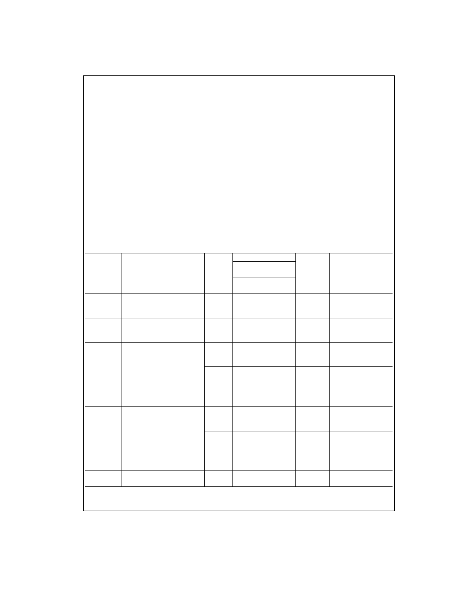
DC Characteristics for 'AC Family Devices
54AC
Symbol
Parameter
V
CC
T
A
=
Units
Conditions
(V)
-55∞C to +125∞C
Guaranteed
Limits
V
IH
Minimum High Level
3.0
2.1
V
OUT
= 0.1V
Input Voltage
4.5
3.15
V
or V
CC
- 0.1V
5.5
3.85
V
IL
Maximum Low Level
3.0
0.9
V
OUT
= 0.1V
Input Voltage
4.5
1.35
V
or V
CC
- 0.1V
5.5
1.65
V
OH
Minimum High Level
3.0
2.9
I
OUT
= -50 µA
Output Voltage
4.5
4.4
V
5.5
5.4
(Note 2)
V
IN
= V
IL
or V
IH
3.0
2.4
I
OH
= -12 mA
4.5
3.7
V
I
OH
= -24 mA
5.5
4.7
I
OH
= -24 mA
V
OL
Maximum Low Level
3.0
0.1
I
OUT
= 50 µA
Output Voltage
4.5
0.1
V
5.5
0.1
(Note 2)
V
IN
= V
IL
or V
IH
3.0
0.50
I
OL
= 12 mA
4.5
0.50
V
I
OL
= 24 mA
5.5
0.50
I
OL
= 24 mA
I
IN
Maximum Input
5.5
±
1.0
µA
V
I
= V
CC
, GND
Leakage Current
www.national.com
4

DC Characteristics for 'AC Family Devices
(Continued)
54AC
Symbol
Parameter
V
CC
T
A
=
Units
Conditions
(V)
-55∞C to +125∞C
Guaranteed
Limits
I
OLD
Minimum Dynamic
Output Current (Note 3)
5.5
50
mA
V
OLD
= 1.65V Max
I
OHD
5.5
-50
mA
V
OHD
= 3.85V Min
I
CC
Maximum Quiescent
5.5
80.0
µA
V
IN
= V
CC
Supply Current
or GND
Note 2: All outputs loaded; thresholds on input associated with output under test.
Note 3: Maximum test duration 2.0 ms, one output loaded at a time.
Note 4: I
IN
and I
CC
@
3.0V are guaranteed to be less than or equal to the respective limit
@
5.5V V
CC
.
I
CC
for 54AC
@
25∞C is identical to 74AC
@
25∞C.
DC Characteristics for 'ACT Family Devices
54ACT
Symbol
Parameter
V
CC
T
A
=
Units
Conditions
(V)
-55∞C to +125∞C
Guaranteed
Limits
V
IH
Minimum High Level
4.5
2.0
V
V
OUT
= 0.1V
Input Voltage
5.5
2.0
or V
CC
- 0.1V
V
IL
Maximum Low Level
4.5
0.8
V
V
OUT
= 0.1V
Input Voltage
5.5
0.8
or V
CC
- 0.1V
V
OH
Minimum High Level
4.5
4.4
V
I
OUT
= -50 µA
Output Voltage
5.5
5.4
(Note 5)
V
IN
= V
IL
or V
IH
4.5
3.70
V
I
OH
= -24 mA
5.5
4.70
I
OH
= -24 mA
V
OL
Maximum Low Level
4.5
0.1
V
I
OUT
= 50 µA
Output Voltage
5.5
0.1
(Note 5)
V
IN
= V
IL
or V
IH
4.5
0.50
V
I
OL
= 24 mA
5.5
0.50
I
OL
= 24 mA
I
IN
Maximum Input
5.5
±
1.0
µA
V
I
= V
CC
, GND
Leakage Current
I
CCT
Maximum
5.5
1.6
mA
V
I
= V
CC
- 2.1V
I
CC
/Input
I
OLD
Minimum Dynamic
Output Current (Note 6)
5.5
50
mA
V
OLD
= 1.65V Max
I
OHD
5.5
-50
mA
V
OHD
= 3.85V Min
I
CC
Maximum Quiescent
5.5
80.0
µA
V
IN
= V
CC
Supply Current
or GND
Note 5: All outputs loaded; thresholds on input associated with output under test.
Note 6: Maximum test duration 2.0 ms, one output loaded at a time.
Note 7: I
CC
for 54ACT
@
25∞C is identical to 74ACT
@
25∞C.
5
www.national.com