 | –≠–ª–µ–∫—Ç—Ä–æ–Ω–Ω—ã–π –∫–æ–º–ø–æ–Ω–µ–Ω—Ç: 54AC244L | –°–∫–∞—á–∞—Ç—å:  PDF PDF  ZIP ZIP |
54AC244
∑
54ACT244
Octal Buffer/Line Driver with TRI-STATE
Æ
Outputs
General Description
The 'AC/'ACT244 is an octal buffer and line driver designed
to be employed as a memory address driver, clock driver and
bus-oriented transmitter/receiver which provides improved
PC board density.
Features
n
I
CC
and I
OZ
reduced by 50%
n
TRI-STATE outputs drive bus lines or buffer memory
address registers
n
Outputs source/sink 24 mA
n
'ACT244 has TTL-compatible inputs
n
Standard Microcircuit Drawing (SMD)
-- 'AC244: 5962-87552
-- 'ACT244: 5962-87760
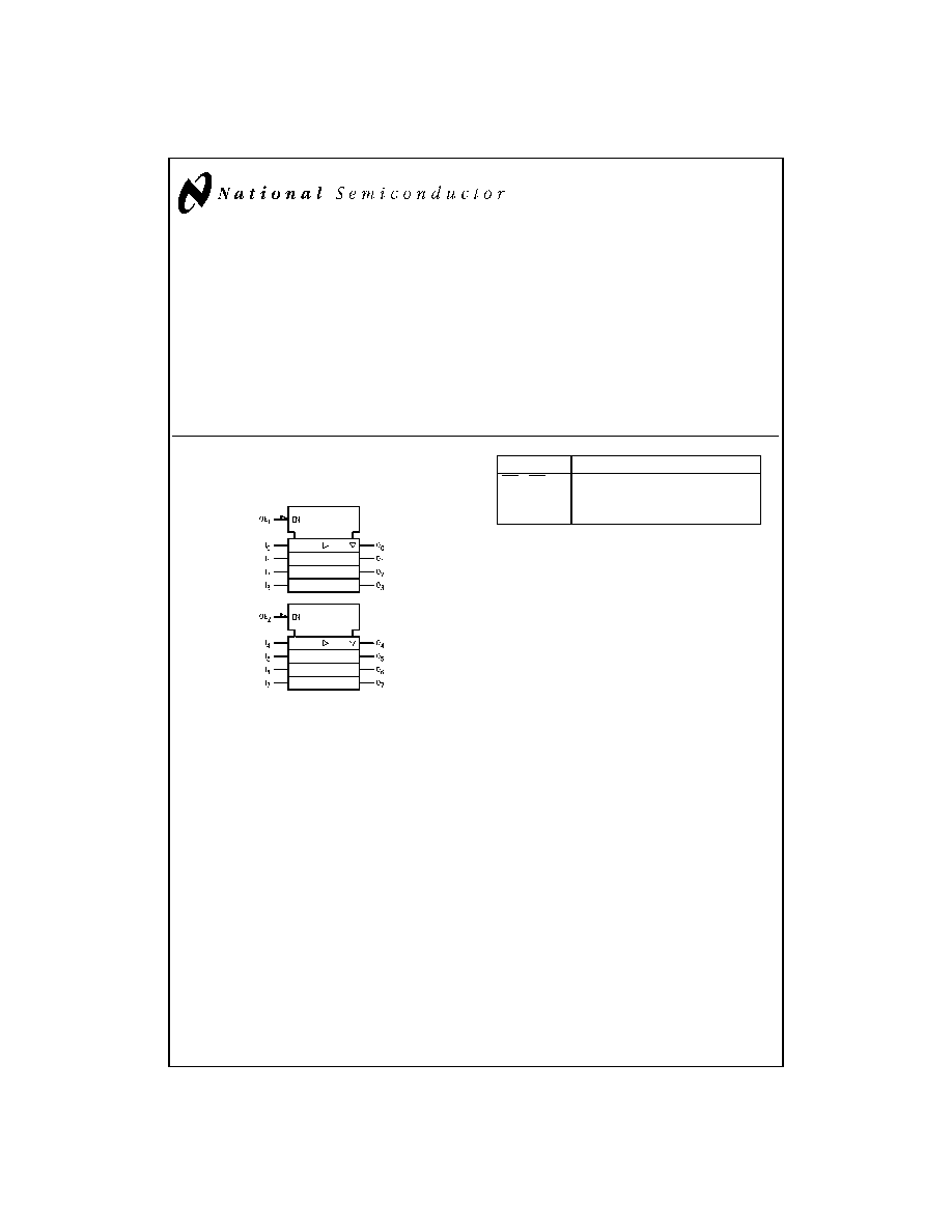
Logic Symbol
Pin Names
Description
OE
1
, OE
2
TRI-STATE Output Enable Inputs
I
0
≠I
7
Inputs
O
0
≠O
7
Outputs
TRI-STATE
Æ
is a registered trademark of National Semiconductor Corporation.
FACT
Æ
is a registered trademark of Fairchild Semiconductor Corporation.
IEEE/IEC
DS100282-1
August 1998
54AC244
∑
54ACT244
Octal
Buffer/Line
Driver
with
TRI-ST
A
T
E
Outputs
© 1998 National Semiconductor Corporation
DS100282
www.national.com
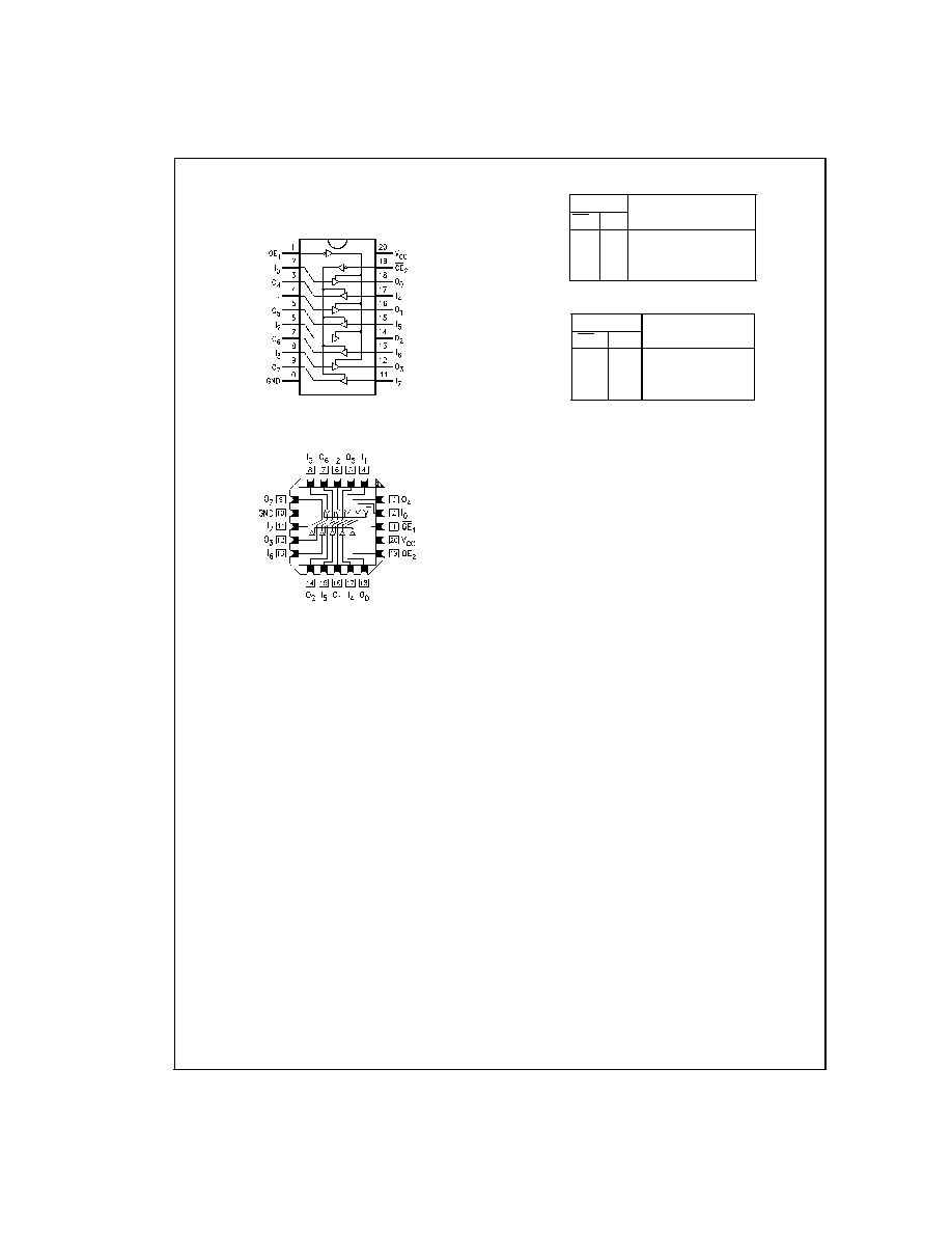
Connection Diagrams
Truth Tables
Inputs
Outputs
OE
1
I
n
(Pins 12, 14, 16, 18)
L
L
L
L
H
H
H
X
Z
H = HIGH Voltage Level
L = LOW Voltage Level
Inputs
Outputs
OE
2
I
n
(Pins 3, 5, 7, 9)
L
L
L
L
H
H
H
X
Z
X = Immaterial
Z = High Impedance
Pin Assignment for DIP
and Flatpak
DS100282-2
Pin Assignment for LCC
DS100282-3
www.national.com
2
Absolute Maximum Ratings
(Note 1)
If Military/Aerospace specified devices are required,
please contact the National Semiconductor Sales Office/
Distributors for availability and specifications.
Supply Voltage (V
CC
)
-0.5V to +7.0V
DC Input Diode Current (I
IK
)
V
I
= -0.5V
-20 mA
V
I
= V
CC
+ 0.5V
+20 mA
DC Input Voltage (V
I
)
-0.5V to V
CC
+ 0.5V
DC Output Diode Current (I
OK
)
V
O
= -0.5V
-20 mA
V
O
= V
CC
+ 0.5V
+20 mA
DC Output Voltage (V
O
)
-0.5V to V
CC
+ 0.5V
DC Output Source
or Sink Current (I
O
)
±
50 mA
DC V
CC
or Ground Current
per Output Pin (I
CC
or I
GND
)
±
50 mA
Storage Temperature (T
STG
)
-65∞C to +150∞C
Junction Temperature (T
J
)
CDIP
175∞C
Recommended Operating
Conditions
Supply Voltage (V
CC
)
'AC
2.0V to 6.0V
'ACT
4.5V to 5.5V
Input Voltage (V
I
)
0V to V
CC
Output Voltage (V
O
)
0V to V
CC
Operating Temperature (T
A
)
54AC/ACT
-55∞C to +125∞C
Minimum Input Edge Rate (
V/
t)
'AC Devices
V
IN
from 30% to 70% of V
CC
V
CC
@
3.3V, 4.5V, 5.5V
125 mV/ns
Minimum Input Edge Rate (
V/
t)
'ACT Devices
V
IN
from 0.8V to 2.0V
V
CC
@
4.5V, 5.5V
125 mV/ns
Note 1: Absolute maximum ratings are those values beyond which damage
to the device may occur. The databook specifications should be met, without
exception, to ensure that the system design is reliable over its power supply,
temperature, and output/input loading variables. National does not recom-
mend operation of FACT
Æ
circuits outside databook specifications.
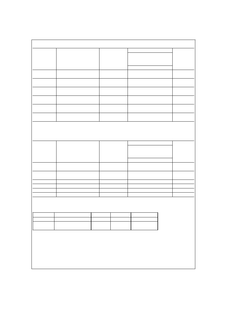
DC Characteristics for 'AC Family Devices
54AC
Symbol
Parameter
V
CC
T
A
=
Units
Conditions
(V)
-55∞C to +125∞C
Guaranteed Limits
V
IH
Minimum High
3.0
2.1
V
OUT
= 0.1V
Level Input
4.5
3.15
V
or V
CC
- 0.1V
Voltage
5.5
3.85
V
IL
Maximum Low
3.0
0.9
V
OUT
= 0.1V
Level Input
4.5
1.35
V
or V
CC
- 0.1V
Voltage
5.5
1.65
V
OH
Minimum High
3.0
2.9
I
OUT
= -50 µA
Level Output
4.5
4.4
V
Voltage
5.5
5.4
(Note 2)
V
IN
= V
IL
or V
IH
3.0
2.4
-12 mA
4.5
3.7
V
I
OH
-24 mA
5.5
4.7
-24 mA
V
OL
Maximum Low
3.0
0.1
I
OUT
= 50 µA
Level Output
4.5
0.1
V
Voltage
5.5
0.1
(Note 2)
V
IN
= V
IL
or V
IH
3.0
0.50
12 mA
4.5
0.50
V
I
OL
24 mA
5.5
0.50
24 mA
I
IN
Maximum Input
5.5
±
1.0
µA
V
I
= V
CC
, GND
Leakage Current
3
www.national.com
DC Characteristics for 'AC Family Devices
(Continued)
54AC
Symbol
Parameter
V
CC
T
A
=
Units
Conditions
(V)
-55∞C to +125∞C
Guaranteed Limits
I
OZ
Maximum
V
I
(OE) = V
IL
, V
IH
TRI-STATE
5.5
±
5.0
µA
V
I
= V
CC
, V
GND
Current
V
O
= V
CC
, GND
I
OLD
(Note 3) Minimum
Dynamic Output
Current
5.5
50
mA
V
OLD
= 1.65V Max
I
OHD
5.5
-50
mA
V
OHD
= 3.85V Min
I
CC
Maximum Quiescent
5.5
80.0
µA
V
IN
= V
CC
Supply Current
or GND
Note 2: All outputs loaded; thresholds on input associated with output under test.
Note 3: Maximum test duration 2.0 ms, one output loaded at a time.
Note 4: I
IN
and I
CC
@
3.0V are guaranteed to be less than or equal to the respective limit
@
5.5V V
CC
.
Note 5: I
CC
for 54AC
@
25∞C is identical to 74AC
@
25∞C.
DC Characteristics for 'ACT Family Devices
54ACT
Symbol
Parameter
V
CC
T
A
=
Units
Conditions
(V)
-55∞C to +125∞C
Guaranteed Limits
V
IH
Minimum High Level
4.5
2.0
V
V
OUT
= 0.1V
Input Voltage
5.5
2.0
or V
CC
- 0.1V
V
IL
Maximum Low Level
4.5
0.8
V
V
OUT
= 0.1V
Input Voltage
5.5
0.8
or V
CC
- 0.1V
V
OH
Minimum High Level
4.5
4.4
V
I
OUT
= -50 µA
Output Voltage
5.5
5.4
(Note 6)
V
IN
= V
IL
or V
IH
4.5
3.70
V
I
OH
-24 mA
5.5
4.70
-24 mA
V
OL
Maximum Low Level
4.5
0.1
V
I
OUT
= 50 µA
Output Voltage
5.5
0.1
(Note 6)
V
IN
= V
IL
or V
IH
4.5
0.50
V
I
OL
24 mA
5.5
0.50
24 mA
I
IN
Maximum Input Leakage Current
5.5
±
1.0
µA
V
I
= V
CC
, GND
I
OZ
Maximum TRI-STATE
5.5
±
5.0
µA
V
I
= V
IL
, V
IH
Current
V
O
= V
CC
, GND
I
CCT
Maximum I
CC
/Input
5.5
1.6
mA
V
I
= V
CC
- 2.1V
I
OLD
(Note 7) Minimum
Dynamic Output
Current
5.5
50
mA
V
OLD
= 1.65V Max
I
OHD
5.5
-50
mA
V
OHD
= 3.85V Min
I
CC
Maximum Quiescent
5.5
80.0
µA
V
IN
= V
CC
Supply Current
or GND
Note 6: All outputs loaded; thresholds on input associated with output under test.
Note 7: Maximum test duration 2.0 ms, one output loaded at a time.
Note 8: I
CC
for 54ACT
@
25∞C is identical to 74ACT
@
25∞C.
www.national.com
4
AC Electrical Characteristics
54AC
V
CC
T
A
= -55∞C
Symbol
Parameter
(V)
to +125∞C
Units
(Note 9)
C
L
= 50 pF
Min
Max
t
PLH
Propagation Delay
3.3
1.0
12.5
ns
Data to Output
5.0
1.0
9.5
t
PHL
Propagation Delay
3.3
1.0
12.0
ns
Data to Output
5.0
1.0
9.0
t
PZH
Output Enable Time
3.3
1.0
11.5
ns
5.0
1.0
9.0
t
PZL
Output Enable Time
3.3
1.0
13.0
ns
5.0
1.0
10.5
t
PHZ
Output Disable Time
3.3
1.0
12.5
ns
5.0
1.0
10.5
t
PLZ
Output Disable Time
3.3
1.0
13.0
ns
5.0
1.0
11.0
Note 9: Voltage Range 3.3 is 3.3V
±
0.3V
Voltage Range 5.0 is 5.0V
±
0.5V
AC Electrical Characteristics
54ACT
V
CC
T
A
= -55∞C
Symbol
Parameter
(V)
to +125∞C
Units
(Note 10)
C
L
= 50 pF
Min
Max
t
PLH
Propagation Delay
5.0
1.0
10.0
ns
Data to Output
t
PHL
Propagation Delay
5.0
1.0
10.0
ns
Data to Output
t
PZH
Output Enable Time
5.0
1.0
9.5
ns
t
PZL
Output Enable Time
5.0
1.0
11.0
ns
t
PHZ
Output Disable Time
5.0
1.0
11.0
ns
t
PLZ
Output Disable Time
5.0
1.0
11.5
ns
Note 10: Voltage Range 5.0 is 5.0V
±
0.5V
Capacitance
Symbol
Parameter
Typ
Units
Conditions
C
IN
Input Capacitance
4.5
pF
V
CC
= OPEN
C
PD
Power Dissipation
45.0
pF
V
CC
= 5.0V
Capacitance
5
www.national.com