 | –≠–ª–µ–∫—Ç—Ä–æ–Ω–Ω—ã–π –∫–æ–º–ø–æ–Ω–µ–Ω—Ç: 54AC373 | –°–∫–∞—á–∞—Ç—å:  PDF PDF  ZIP ZIP |
54AC373
∑
54ACT373
Octal Transparent Latch with TRI-STATE
Æ
Outputs
General Description
The 'AC/'ACT373 consists of eight latches with TRI-STATE
outputs for bus organized system applications. The flip-flops
appear transparent to the data when Latch Enable (LE) is
HIGH. When LE is LOW, the data that meets the setup time
is latched. Data appears on the bus when the Output Enable
(OE) is LOW. When OE is HIGH, the bus output is in the high
impedance state.
Features
n
I
CC
and I
OZ
reduced by 50%
n
Eight latches in a single package
n
TRI-STATE outputs for bus interfacing
n
Outputs source/sink 24 mA
n
'ACT373 has TTL-compatible inputs
n
Standard Microcircuit Drawing (SMD)
-- 'AC373: 5962-87555
-- 'ACT373: 5962-87556
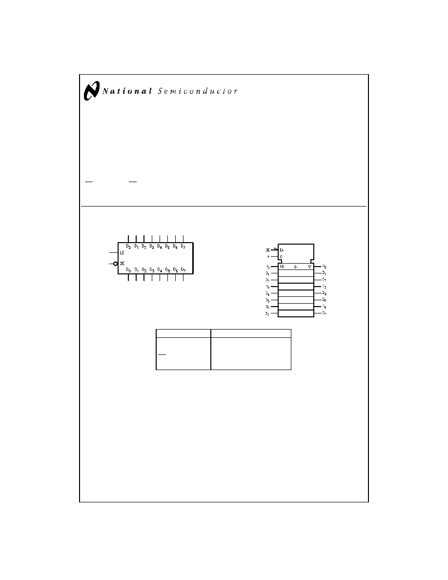
Logic Symbols
Pin Names
Description
D
0
≠D
7
Data Inputs
LE
Latch Enable Input
OE
Output Enable Input
O
0
≠O
7
TRI-STATE Latch Outputs
TRI-STATE
Æ
is a registered trademark of National Semiconductor Corporation.
FACT
Æ
is a registered trademark of Fairchild Semiconductor Corporation.
DS100329-1
IEEE/IEC
DS100329-2
August 1998
54AC373
∑
54ACT373
Octal
T
ransparent
Latch
with
TRI-ST
A
T
E
Outputs
© 1998 National Semiconductor Corporation
DS100329
www.national.com
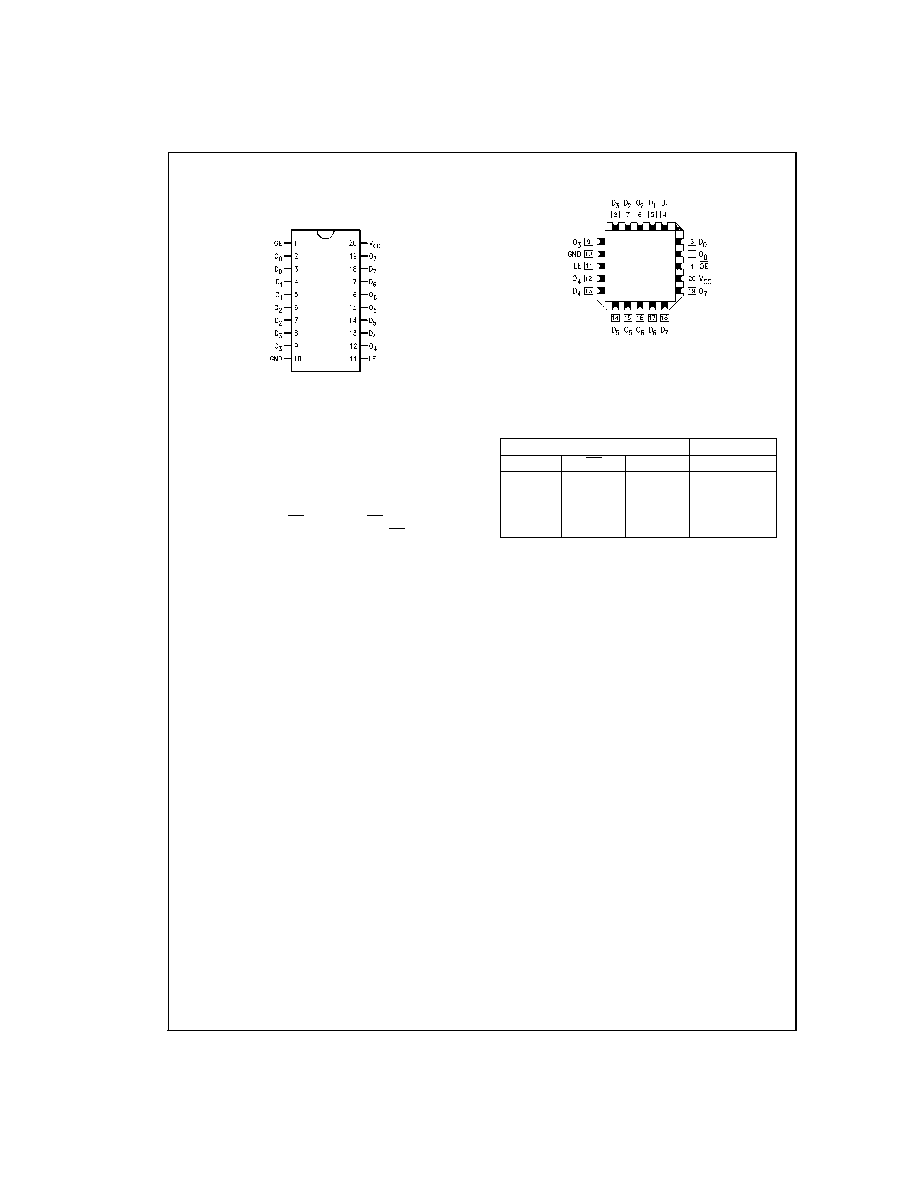
Connection Diagrams
Functional Description
The 'AC/'ACT373 contains eight D-type latches with
TRI-STATE standard outputs. When the Latch Enable (LE)
input is HIGH, data on the D
n
inputs enters the latches. In
this condition the latches are transparent, i.e., a latch output
will change state each time its D input changes. When LE is
LOW, the latches store the information that was present on
the D inputs a setup time preceding the HIGH-to-LOW tran-
sition of LE. The TRI-STATE standard outputs are controlled
by the Output Enable (OE) input. When OE is LOW, the stan-
dard outputs are in the 2-state mode. When OE is HIGH, the
standard outputs are in the high impedance mode but this
does not interfere with entering new data into the latches.
Truth Table
Inputs
Outputs
LE
OE
D
n
O
n
X
H
X
Z
H
L
L
L
H
L
H
H
L
L
X
O
0
H = HIGH Voltage Level
L = LOW Voltage Level
Z = High Impedance
X = Immaterial
O
0
= Previous O
0
before HIGH to Low transition of Latch Enable
Pin Assignment for DIP
and Flatpak
DS100329-3
Pin Assignment for LCC
DS100329-4
www.national.com
2
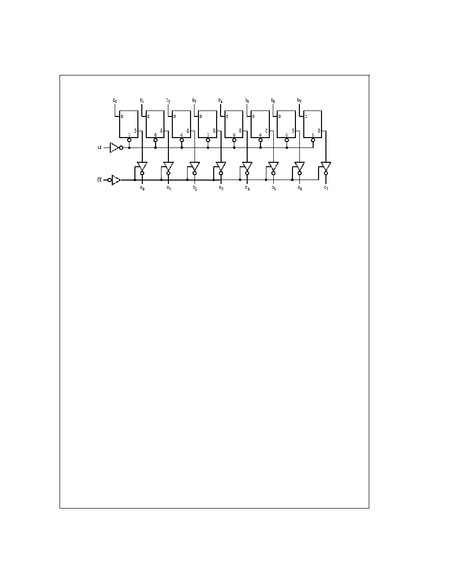
Logic Diagram
DS100329-5
Please note that this diagram is provided only for the understanding of logic operations and should not be used to estimate propagation delays.
3
www.national.com

Absolute Maximum Ratings
(Note 1)
If Military/Aerospace specified devices are required,
please contact the National Semiconductor Sales Office/
Distributors for availability and specifications.
Supply Voltage (V
CC
)
-0.5V to +7.0V
DC Input Diode Current (I
IK
)
V
I
= -0.5V
-20 mA
V
I
= V
CC
+ 0.5V
+20 mA
DC Input Voltage (V
I
)
-0.5V to V
CC
+ 0.5V
DC Output Diode Current (I
OK
)
V
O
= -0.5V
-20 mA
V
O
= V
CC
+ 0.5V
+20 mA
DC Output Voltage (V
O
)
-0.5V to V
CC
+ 0.5V
DC Output Source
or Sink Current (I
O
)
±
50 mA
DC V
CC
or Ground Current
per Output Pin (I
CC
or I
GND
)
±
50 mA
Storage Temperature (T
STG
)
-65∞C to +150∞C
Junction Temperature (T
J
)
CDIP
175∞C
Recommended Operating
Conditions
Supply Voltage (V
CC
)
'AC
2.0V to 6.0V
'ACT
4.5V to 5.5V
Input Voltage (V
I
)
0V to V
CC
Output Voltage (V
O
)
0V to V
CC
Operating Temperature (T
A
)
54AC/ACT
-55∞C to +125∞C
Minimum Input Edge Rate (
V/
t)
'AC Devices
V
IN
from 30% to 70% of V
CC
V
CC
@
3.3V, 4.5V, 5.5V
125 mV/ns
Minimum Input Edge Rate (
V/
t)
'ACT Devices
V
IN
from 0.8V to 2.0V
V
CC
@
4.5V, 5.5V
125 mV/ns
Note 1: Absolute maximum ratings are those values beyond which damage
to the device may occur. The databook specifications should be met, without
exception, to ensure that the system design is reliable over its power supply,
temperature, and output/input loading variables. National does not recom-
mend operation of FACT
Æ
circuits outside databook specifications.
DC Characteristics for 'AC Family Devices
54AC
Symbol
Parameter
V
CC
T
A
=
Units
Conditions
(V)
-55∞C to +125∞C
Guaranteed Limits
V
IH
Minimum High
3.0
2.1
V
OUT
= 0.1V
Level Input
4.5
3.15
V
or V
CC
- 0.1V
Voltage
5.5
3.85
V
IL
Maximum Low
3.0
0.9
V
OUT
= 0.1V
Level Input
4.5
1.35
V
or V
CC
- 0.1V
Voltage
5.5
1.65
V
OH
Minimum High
3.0
2.9
I
OUT
= -50 µA
Level Output
4.5
4.4
V
Voltage
5.5
5.4
(Note 2)
V
IN
= V
IL
or V
IH
3.0
2.4
-12 mA
4.5
3.7
V
I
OH
-24 mA
5.5
4.7
-24 mA
V
OL
Maximum Low
3.0
0.1
I
OUT
= 50 µA
Level Output
4.5
0.1
V
Voltage
5.5
0.1
(Note 2)
V
IN
= V
IL
or V
IH
3.0
0.50
12 mA
4.5
0.50
V
I
OL
24 mA
5.5
0.50
24 mA
I
IN
Maximum Input
5.5
±
1.0
µA
V
I
= V
CC
, GND
Leakage Current
www.national.com
4
DC Characteristics for 'AC Family Devices
(Continued)
54AC
Symbol
Parameter
V
CC
T
A
=
Units
Conditions
(V)
-55∞C to +125∞C
Guaranteed Limits
I
OZ
Maximum
V
I
(OE) = V
IL
, V
IH
TRI-STATE
5.5
±
5.0
µA
V
I
= V
CC
, GND
Current
V
O
= V
CC
, GND
I
OLD
(Note 3) Minimum
Dynamic Output
Current
5.5
50
mA
V
OLD
= 1.65V Max
I
OHD
5.5
-50
mA
V
OHD
= 3.85V Min
I
CC
Maximum Quiescent
5.5
80.0
µA
V
IN
= V
CC
Supply Current
or GND
Note 2: All outputs loaded, thresholds on input associated with output under test.
Note 3: Maximum test duration 2.0 ms, one output loaded at a time.
Note 4: I
IN
and I
CC
@
3.0V are guaranteed to be less than or equal to the respective limit
@
5.5V V
CC
.
I
CC
for 54AC
@
25∞C is identical to 74AC
@
25∞C.
DC Characteristics for 'ACT Family Devices
54ACT
Symbol
Parameter
V
CC
T
A
=
Units
Conditions
(V)
-55∞C to +125∞C
Guaranteed Limits
V
IH
Minimum High Level
4.5
2.0
V
V
OUT
= 0.1V
Input Voltage
5.5
2.0
or V
CC
- 0.1V
V
IL
Maximum Low Level
4.5
0.8
V
V
OUT
= 0.1V
Input Voltage
5.5
0.8
or V
CC
- 0.1V
V
OH
Minimum High Level
4.5
4.4
V
I
OUT
= -50 µA
Output Voltage
5.5
5.4
(Note 5)
V
IN
= V
IL
or V
IH
4.5
3.70
V
I
OH
-24 mA
5.5
4.70
-24 mA
V
OL
Maximum Low Level
4.5
0.1
V
I
OUT
= 50 µA
Output Voltage
5.5
0.1
(Note 5)
V
IN
= V
IL
or V
IH
4.5
0.50
V
I
OL
24 mA
5.5
0.50
24 mA
I
IN
Maximum Input Leakage
Current
5.5
±
1.0
µA
V
I
= V
CC
, GND
I
OZ
Maximum TRI-STATE
5.5
±
5.0
µA
V
I
= V
IL
, V
IH
Current
V
O
= V
CC
, GND
I
CCT
Maximum I
CC
/Input
5.5
1.6
mA
V
I
= V
CC
- 2.1V
I
OLD
(Note 6) Minimum Dynamic
5.5
50
mA
V
OLD
= 1.65V Max
I
OHD
Output Current
5.5
-50
mA
V
OHD
= 3.85V Min
I
CC
Maximum Quiescent
5.5
80.0
µA
V
IN
= V
CC
Supply Current
or GND
Note 5: All outputs loaded; thresholds on input associated with output under test.
Note 6: Maximum test duration 2.0 ms, one output loaded at a time.
Note 7: I
CC
for 54ACT
@
25∞C is identical to 74ACT
@
25∞C.
5
www.national.com