54ACT283
4-Bit Binary Full Adder with Fast Carry
General Description
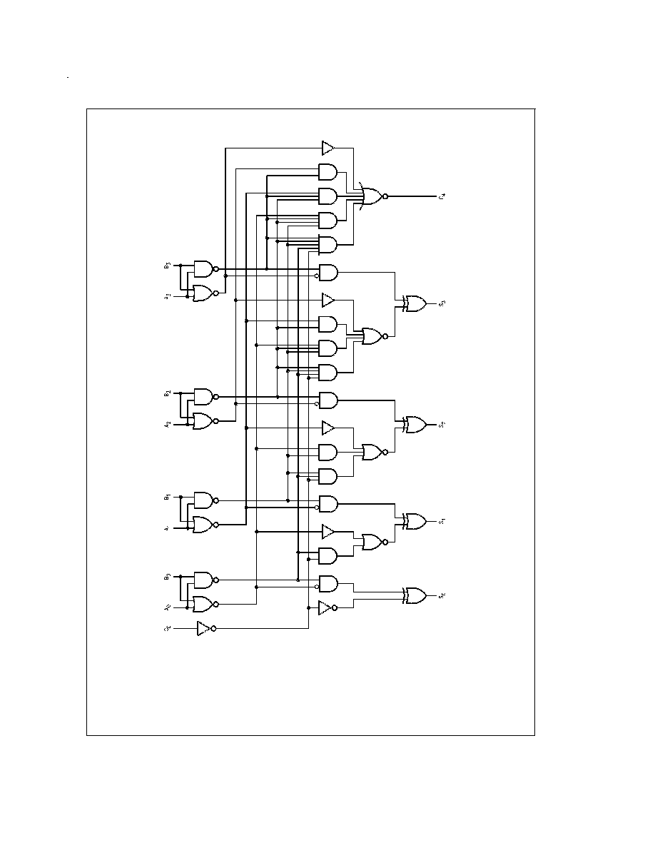
The 'ACT283 high-speed 4-bit binary full adder with internal
carry lookahead accepts two 4-bit binary words (A
0
≠A
3
,
B
0
≠B
3
) and a Carry input (C
0
). It generates the binary Sum
outputs (S
0
≠S
3
) and the Carry output (C
4
) from the most sig-
nificant bit. The 'ACT283 will operate with either active HIGH
or active LOW operands (positive or negative logic).
Features
n
Guaranteed 4000V minimum ESD protection
n
Outputs source/sink 24 mA
n
TTL-compatible inputs
n
Available to Mil-Std-883
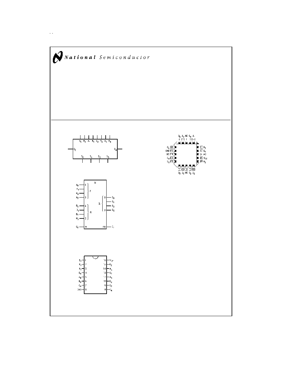
Logic Symbols
Connection Diagrams
Functional Description
The 'ACT283 adds two 4-bit binary words (A plus B) plus the
incoming Carry (C
0
). The binary sum appears on the Sum
(S
0
≠S
3
) and outgoing carry (C
4
) outputs. The binary weight
of the various inputs and outputs is indicated by the subscript
numbers, representing powers of two.
2
0
(A
0
+ B
0
+ C
0
) + 2
1
(A
1
+ B
1
)
+ 2
2
(A
2
+ B
2
) + 2
3
(A
3
+ B
3
)
= S
0
+ 2S
1
+ 4S
2
+ 8S
3
+ 16C
4
Where (+) = plus
Interchanging inputs of equal weight does not affect the op-
eration. Thus C
0
, A
0
, B
0
can be arbitrarily assigned to pins 5,
6 and 7 for DIPS, and 7, 8 and 9 for chip carrier packages.
Due to the symmetry of the binary add function, the 'ACT283
can be used either with all inputs and outputs active HIGH
(positive logic) or with all inputs and outputs active LOW
(negative logic). See
Figure 1. Note that if C
0
is not used it
must be tied LOW for active HIGH logic or tied HIGH for ac-
tive LOW logic.
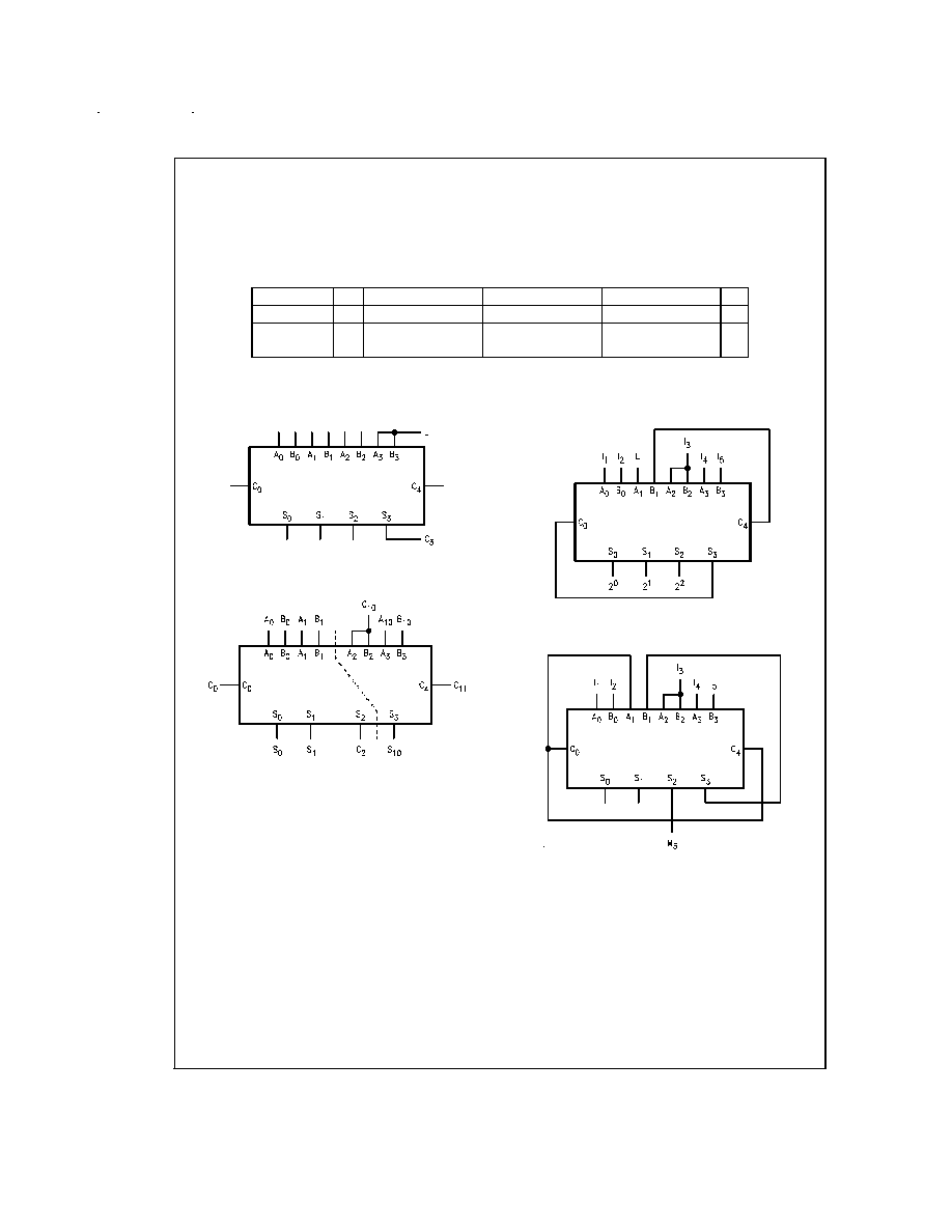
Due to pin limitations, the intermediate carries of the
'ACT283 are not brought out for use as inputs or outputs.
However, other means can be used to effectively insert a
carry into, or bring a carry out from, an intermediate stage.
Figure 2 shows how to make a 3-bit adder. Tying the oper-
and inputs of the fourth adder (A
3
, B
3
) LOW makes S
3
de-
pendent only on, and equal to, the carry from the third adder.
Using somewhat the same principle,
Figure 3 shows a way
of dividing the 'ACT283 into a 2-bit and a 1-bit adder. The
third stage adder (A
2
, B
2
, S
2
) is used merely as a means of
getting a carry (C
10
) signal into the fourth stage (via A
2
and
B
2
) and bringing out the carry from the second stage on S
2
.
DS100977-1
IEEE/IEC
DS100977-4
Pin Assignment
for DIP and Flatpak
DS100977-2
Pin Assignment for LCC
DS100977-3
September 1998
54ACT283
4-Bit
Binary
Full
Adder
with
Fast
Carry
© 1998 National Semiconductor Corporation
DS100977
www.national.com
Functional Description
(Continued)
Note that as long as A
2
and B
2
are the same, whether HIGH
or LOW, they do not influence S
2
. Similarly, when A
2
and B
2
are the same the carry into the third stage does not influence
the carry out of the third stage.
Figure 4 shows a method of
implementing a 5-input encoder, where the inputs are
equally weighted. The outputs S
0
, S
1
and S
2
present a bi-
nary number equal to the number of inputs I
1
≠I
5
that are
true.
Figure 5 shows one method of implementing a 5-input
majority gate. When three or more of the inputs I
1
≠I
5
are
true, the output M
5
is true.
C
0
A
0
A
1
A
2
A
3
B
0
B
1
B
2
B
3
S
0
S
1
S
2
S
3
C
4
Logic Levels
L
L
H
L
H
H
L
L
H
H
H
L
L
H
Active HIGH
0
0
1
0
1
1
0
0
1
1
1
0
0
1
Active LOW
1
1
0
1
0
0
1
1
0
0
0
1
1
0
Active HIGH: 0 + 10 + 9 = 3 + 16
Active LOW: 1 + 5 + 6 = 12 + 0
FIGURE 1. Active HIGH versus Active LOW Interpretation
DS100977-5
FIGURE 2. 3-Bit Adder
DS100977-6
FIGURE 3. 2-Bit and 1-Bit Adders
DS100977-7
FIGURE 4. 5-Input Encoder
DS100977-8
FIGURE 5. 5-Input Majority Gate
www.national.com
2
Absolute Maximum Ratings
(Note 1)
If Military/Aerospace specified devices are required,
please contact the National Semiconductor Sales Office/
Distributors for availability and specifications.
Storage Temperature
-65∞C to +150∞C
Ambient Temperature under Bias
-55∞C to +125∞C
Junction Temperature under Bias
-55∞C to +175∞C
V
CC
Pin Potential to
Ground Pin
-0.5V to +7.0V
Input Voltage (Note 2)
-0.5V to +7.0V
Input Current (Note 2)
-30 mA to +5.0 mA
Voltage Applied to Output
in HIGH State (with V
CC
= 0V)
Standard Output
-0.5V to V
CC
3-STATE Output
-0.5V to +5.5V
Current Applied to Output
in LOW State (Max)
twice the rated I
OL
(mA)
Recommended Operating
Conditions
Free Air Ambient Temperature
Military
-55∞C to +125∞C
Supply Voltage
Military
+4.5V to +5.5V
Note 1: Absolute maximum ratings are values beyond which the device may
be damaged or have its useful life impaired. Functional operation under these
conditions is not implied.
Note 2: Either voltage limit or current limit is sufficient to protect inputs.
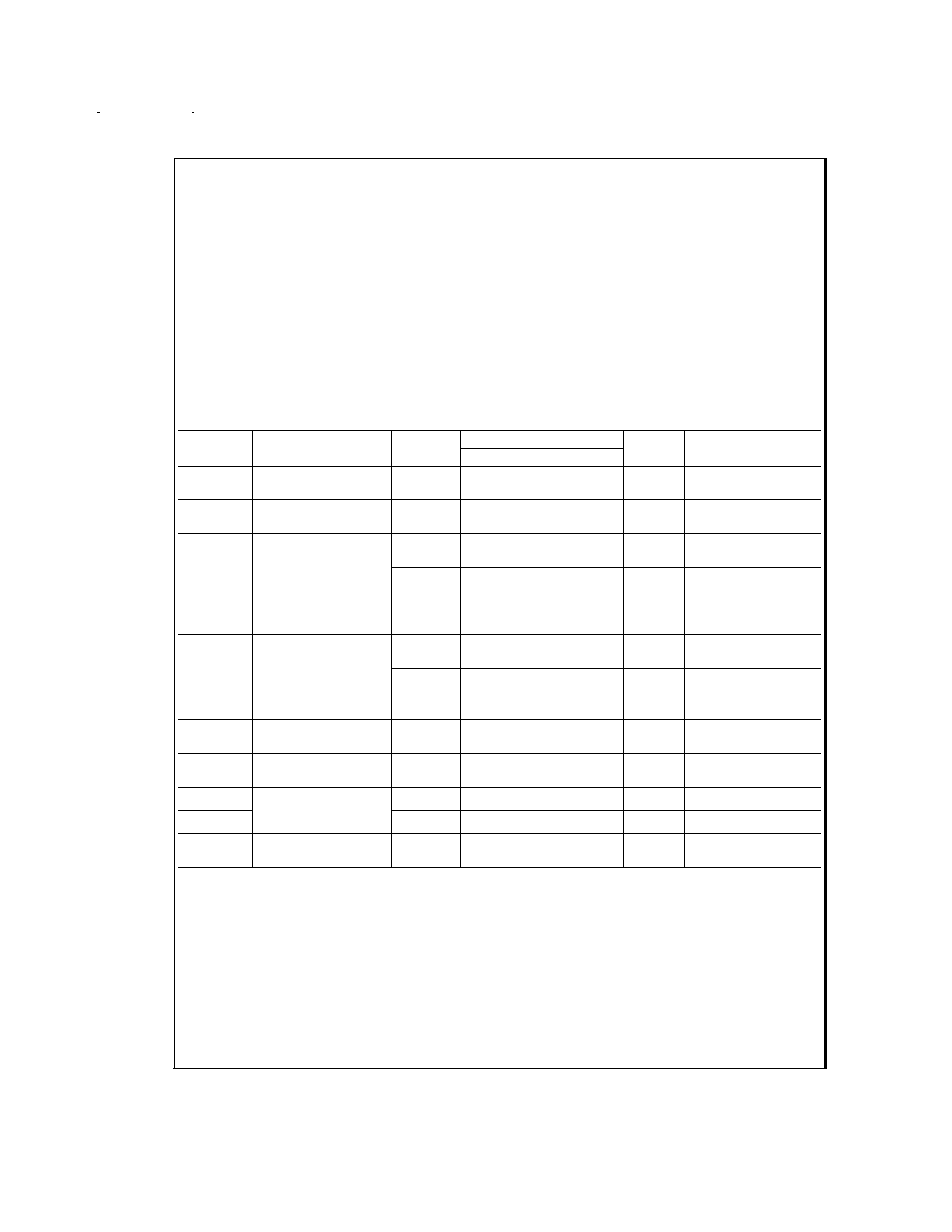
DC Electrical Characteristics for 'ACT Family Devices
Symbol
Parameter
V
CC
T
A
= -55∞C to +125∞C
Units
Conditions
(V)
Guaranteed Limits
V
IH
Minimum High Level
4.5
2.0
V
V
OUT
= 0.1V
Input Voltage
5.5
2.0
or V
CC
- 0.1V
V
IL
Maximum Low Level
4.5
0.8
V
V
OUT
= 0.1V
Input Voltage
5.5
0.8
or V
CC
- 0.1V
V
OH
Minimum High Level
4.5
4.4
V
I
OUT
= -50 µA
Output Voltage
5.5
5.4
V
IN
= V
IL
or V
IH
4.5
3.7
V
I
OH
= -24 mA
5.5
4.7
I
OH
= -24 mA
(Note 3)
V
OL
Maximum Low Level
4.5
0.1
V
I
OUT
= 50 µA
Output Voltage
5.5
0.1
V
IN
= V
IL
or V
IH
4.5
0.5
V
I
OL
= 24 mA
5.5
0.5
I
OL
= 24 mA (Note 3)
I
IN
Maximum Input
5.5
±
1.0
µA
V
I
= V
CC
, GND
Leakage Current
I
CCT
Maximum
5.5
1.6
mA
V
I
= V
CC
- 2.1V
I
CC
/Input
I
OLD
Minimum Dynamic
Output Current
(Note 4)
5.5
50
mA
V
OLD
= 1.65V Max
I
OHD
5.5
-50
mA
V
OHD
= 3.85V Min
I
CC
Maximum Quiescent
5.5
160.0
µA
V
IN
= V
CC
Supply Current
or GND
Note 3: All outputs loaded; thresholds on input associated with output under test.
Note 4: Maximum test duration 2.0 ms, one output loaded at a time.
www.national.com
4