54ACT825
8-Bit D Flip-Flop
General Description
The 'ACT825 is an 8-bit buffered register. They have Clock
Enable and Clear features which are ideal for parity bus in-
terfacing in high performance microprogramming systems.
Also included are multiple enables that allow multi-use con-
trol of the interface. The 'ACT825 has noninverting outputs
and is fully compatible with AMD's Am29825.
Features
n
Outputs source/sink 24 mA
n
Inputs and outputs are on opposite sides
n
'ACT825 has TTL-compatible inputs
n
Standard Microcircuit Drawing (SMD)
-- 'ACT825: 5962-91611
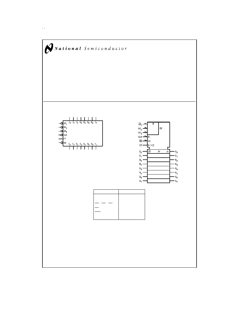
Logic Symbols
Pin Names
Description
D
0
≠D
7
Data Inputs
O
0
≠O
7
Data Outputs
OE
1
, OE
2
, OE
3
Output Enables
EN
Clock Enable
CLR
Clear
CP
Clock Input
FACT
TM
is a trademark of Fairchild Semiconductor.
TRI-STATE
Æ
is a registered trademark of National Semiconductor Corporation.
DS100254-1
IEEE/IEC
DS100254-3
February 1999
54ACT825
8-Bit
D
Flip-Flop
© 1999 National Semiconductor Corporation
DS100254
www.national.com

Connection Diagrams
Functional Description
The 'ACT825 consists of eight D-type edge-triggered
flip-flops. These devices have TRI-STATE
Æ
outputs for bus
systems, organized in a broadside pinning. In addition to the
clock and output enable pins, the buffered clock (CP) and
buffered Output Enable (OE) are common to all flip-flops.
The flip-flops will store the state of their individual D inputs
that meet the setup and hold time requirements on the
LOW-to-HIGH CP transition. With OE
1
, OE
2
and OE
3
LOW,
the contents of the flip-flops are available at the outputs.
When one of OE
1
, OE
2
or OE
3
is HIGH, the outputs go to the
high impedance state.
Operation of the OE input does not affect the state of the
flip-flops. The 'ACT825 has Clear (CLR) and Clock Enable
(EN) pins. These pins are ideal for parity bus interfacing in
high performance systems.
When CLR is LOW and OE is LOW, the outputs are LOW.
When CLR is HIGH, data can be entered into the flip-flops.
When EN is LOW, data on the inputs is transferred to the
outputs on the LOW-to-HIGH clock transition. When EN is
HIGH, the outputs do not change state, regardless of the
data or clock input transitions.
Function Table
Inputs
Internal
Output
Function
OE
CLR
EN
CP
D
n
Q
O
H
X
L
N
L
L
Z
High-Z
H
X
L
N
H
H
Z
High-Z
H
L
X
X
X
L
Z
Clear
L
L
X
X
X
L
L
Clear
H
H
H
X
X
NC
Z
Hold
L
H
H
X
X
NC
NC
Hold
H
H
L
N
L
L
Z
Load
H
H
L
N
H
H
Z
Load
L
H
L
N
L
L
L
Load
L
H
L
N
H
H
H
Load
H = HIGH Voltage Level
L = LOW Voltage Level
X = Immaterial
Z = High Impedance
N
= LOW-to-HIGH Transition
NC = No Change
Pin Assignment
for DIP and Flatpak
DS100254-2
Pin Assignment for LCC
DS100254-4
www.national.com
2
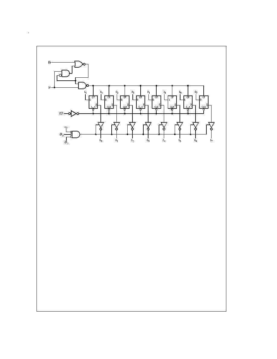
Logic Diagram
DS100254-5
Please note that this diagram is provided only for the understanding of logic operations and should not be used to estimate propagation delays.
www.national.com
3

Absolute Maximum Ratings
(Note 1)
If Military/Aerospace specified devices are required,
please contact the National Semiconductor Sales Office/
Distributors for availability and specifications.
Supply Voltage (V
CC
)
-0.5V to 7.0V
DC Input Diode Current (I
IK
)
V
I
= -0.5V
-20 mA
V
I
= V
CC
+0.5V
+20 mA
DC Input Voltage (V
I
)
-0.5V to V
CC
+0.5V
DC Output Diode Current (I
OK
)
V
O
= -0.5V
-20 mA
V
O
= V
CC
+0.5V
+20 mA
DC Output Voltage (V
O
)
+0.5V
DC Output Source or Sink Current
(I
O
)
±
50 mA
DC V
CC
or Ground Current
Per Output Pin (I
CC
or I
GND
)
±
50 mA
Storage Temperature (T
STG
)
-65∞C to +150∞C
Junction Temperature (T
J
)
CDIP
175∞C
Recommended Operating
Conditions
Supply Voltage (V
CC
)
'ACT
4.5V to 5.5V
Input Voltage (V
I
)
0V to V
CC
Output Voltage (V
O
)
0V to V
CC
Operating Temperature (T
A
)
54ACT
-55∞C to +125∞C
Minimum Input Edge Rate (
V/
t)
'ACT Devices
V
IN
from 0.8V to 2.0V
V
CC
@
4.5V, 5.5V
125 mV/ns
Note 1: Absolute maximum ratings are those values beyond which damage
to the device may occur. The databook specifications should be met, without
exception, to ensure that the system design is reliable over its power supply,
temperature, and output/input loading variables. National does not recom-
mend operation of FACT
TM
circuits outside databook specifications.
DC Electrical Characteristics
54ACT
Symbol
Parameter
V
CC
T
A
=
Units
Conditions
(V)
-55∞C to
+125∞C
Guaranteed
Limits
V
IH
Minimum High Level
4.5
2.0
V
V
OUT
= 0.1V
Input Voltage
5.5
2.0
or V
CC
-0.1V
V
IL
Maximum Low Level
4.5
0.8
V
OUT
= 0.1V
Input Voltage
5.5
0.8
or V
CC
-0.1V
V
OH
Minimum High Level
4.5
4.4
V
I
OUT
= -50 µA
5.5
5.4
(Note 2)
V
IN
= V
IL
or V
IH
4.5
3.70
V
I
OH
= -24 mA
5.5
4.70
I
OH
= -24 mA
V
OL
Maximum Low Level
4.5
0.1
V
I
OUT
= 50 µA
Output Voltage
5.5
0.1
(Note 2)
V
IN
= V
IL
or V
IH
4.5
0.50
V
I
OL
= 24 mA
5.5
0.50
I
OL
= 24 mA
I
IN
Maximum Input Leakage Current
5.5
±
1.0
µA
V
I
= V
CC
, GND
I
OZ
Maximum TRI-STATE Current
5.5
±
10.0
µA
V
I
= V
IL
, V
IH
V
O
= V
CC
, GND
I
CCT
Maximum I
CC
/Input
5.5
1.6
mA
V
I
= V
CC
-2.1V
(Note 3)
I
OLD
Minimum Dynamic
5.5
50
mA
V
OLD
= 1.65V Max
I
OHD
Output Current
5.5
-50
mA
V
OHD
= 3.85V Min
I
CC
Maximum Quiescent
5.5
160
µA
V
IN
= V
CC
Supply Current
or GND
Note 2: All outputs loaded; thresholds on input associated with output under test.
Note 3: Maximum test duration 2.0 ms, one output loaded at a time.
www.national.com
4

DC Electrical Characteristics
(Continued)
Note 4: I
CC
limit for 54ACT
@
25∞C is identical to 74ACT
@
25∞C.
AC Electrical Characteristics
54ACT
V
CC
T
A
= -55∞C
Fig.
Symbol
Parameter
(V)
to +125∞C
Units
No.
(Note 5)
C
L
= 50 pF
Min
Max
f
max
Maximum Clock
5.0
95
MHz
Frequency
t
PLH
Propagation Delay
5.0
1.5
11.5
ns
CP to O
n
t
PHL
Propagation Delay
5.0
1.5
11.5
ns
CP to O
n
t
PHL
Propagation Delay
5.0
1.5
18.0
ns
CLR to O
n
t
PZH
Output Enable Time
5.0
1.5
11.5
ns
OE to O
n
t
PZL
Output Enable Time
5.0
1.5
12.5
ns
OE to O
n
t
PHZ
Output Disable Time
5.0
1.5
13.5
ns
OE to O
n
t
PLZ
Output Disable Time
5.0
1.5
13.0
ns
OE to O
n
Note 5: Voltage Range 5.0 is 5.0V
±
0.5V
AC Operating Requirements
54ACT
V
CC
T
A
= -55∞C
Fig.
Symbol
Parameter
(V)
to +125∞C
Units
No.
(Note 6)
C
L
= 50 pF
Guaranteed
Minimum
t
s
Setup Time, HIGH or LOW
5.0
4.0
ns
D
n
to CP
t
h
Hold Time, HIGH or LOW
5.0
2.5
ns
D
n
to CP
t
s
Setup Time, HIGH or LOW
5.0
4.0
ns
EN to CP
t
h
Hold Time, HIGH or LOW
5.0
2.0
ns
EN to CP
t
w
CP Pulse Width
5.0
6.0
ns
HIGH or LOW
t
w
CLR Pulse Width, LOW
5.0
7.0
ns
t
rec
CLR to CP
5.0
4.5
ns
Recovery Time
Note 6: Voltage Range 5.0 is 5.0V
±
0.5V
www.national.com
5