TL F 9482
54F74F153
Dual
4-Input
Multiplexer
December 1994
54F 74F153
Dual 4-Input Multiplexer
General Description
The 'F153 is a high-speed dual 4-input multiplexer with com-
mon select inputs and individual enable inputs for each sec-
tion It can select two lines of data from four sources The
two buffered outputs present data in the true (non-inverted)
form In addition to multiplexer operation the 'F153 can
generate any two functions of three variables
Features
Y
Guaranteed 4000V minimum ESD protection
Commercial
Military
Package
Package Description
Number
74F153PC
N16E
16-Lead (0 300 Wide) Molded Dual-In-Line
54F153DM (Note 2)
J16A
16-Lead Ceramic Dual-In-Line
74F153SC (Note 1)
M16A
16-Lead (0 150 Wide) Molded Small Outline JEDEC
74F153SJ (Note 1)
M16D
16-Lead (0 300 Wide) Molded Small Outline EIAJ
54F153FM (Note 2)
W16A
16-Lead Cerpack
54F153LM (Note 2)
E20A
20-Lead Ceramic Leadless Chip Carrier Type C
Note 1
Devices also available in 13
reel Use suffix
e
SCX and SJX
Note 2
Military grade device with environmental and burn-in processing Use suffix
e
DMQB FMQB and LMQB
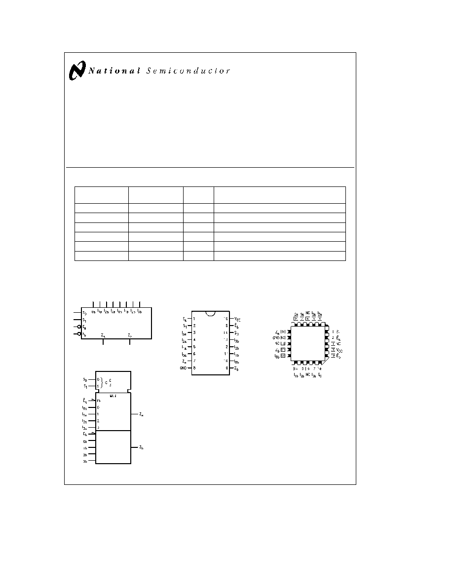
Logic Symbols
Connection Diagrams
TL F 9482 � 3
IEEE IEC
TL F 9482 � 5
Pin Assignment
for DIP SOIC and Flatpak
TL F 9482 � 1
Pin Assignment
for LCC
TL F 9482 � 2
TRI-STATE
is a registered trademark of National Semiconductor Corporation
C1995 National Semiconductor Corporation
RRD-B30M75 Printed in U S A
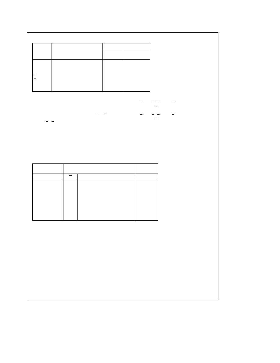
Unit Loading Fan Out
54F 74F
Pin Names
Description
U L
Input I
IH
I
IL
HIGH LOW
Output I
OH
I
OL
I
0a
� I
3a
Side A Data Inputs
1 0 1 0
20 mA
b
0 6 mA
I
0b
� I
3b
Side B Data Inputs
1 0 1 0
20 mA
b
0 6 mA
S
0
S
1
Common Select Inputs
1 0 1 0
20 mA
b
0 6 mA
E
a
Side A Enable Input (Active LOW)
1 0 1 0
20 mA
b
0 6 mA
E
b
Side B Enable Input (Active LOW)
1 0 1 0
20 mA
b
0 6 mA
Z
a
Side A Output
50 33 3
b
1 mA 20 mA
Z
b
Side B Output
50 33 3
b
1 mA 20 mA
Functional Description
The 'F153 is a dual 4-input multiplexer It can select two bits
of data from up to four sources under the control of the
common Select inputs (S
0
S
1
) The two 4-input multiplexer
circuits have individual active LOW Enables (E
a
E
b
) which
can be used to strobe the outputs independently When the
Enables (E
a
E
b
) are HIGH the corresponding outputs (Z
a
Z
b
) are forced LOW The 'F153 is the logic implementation
of a 2-pole 4-position switch where the position of the
switch is determined by the logic levels supplied to the two
Select inputs The logic equations for the outputs are as
follows
Z
a
e
E
a
(I
0a
S
1
S
0
a
I
1a
S
1
S
0
a
I
2a
S
1
S
0
a
I
3a
S
1
S
0
)
Z
b
e
E
b
(I
0b
S
1
S
0
a
I
1b
S
1
S
0
a
I
2b
S
1
S
0
a
I
3b
S
1
S
0
)
The 'F153 can be used to move data from a group of regis-
ters to a common output bus The particular register from
which the data came would be determined by the state of
the Select inputs A less obvious application is as a function
generator The 'F153 can generate two functions of three
variables This is useful for implementing highly irregular
random logic
Truth Table
Select
Inputs (a or b)
Output
Inputs
S
0
S
1
E
I
0
I
1
I
2
I
3
Z
X
X
H
X
X
X
X
L
L
L
L
L
X
X
X
L
L
L
L
H
X
X
X
H
H
L
L
X
L
X
X
L
H
L
L
X
H
X
X
H
L
H
L
X
X
L
X
L
L
H
L
X
X
H
X
H
H
H
L
X
X
X
L
L
H
H
L
X
X
X
H
H
H
e
HIGH Voltage Level
L
e
LOW
X
e
Immaterial
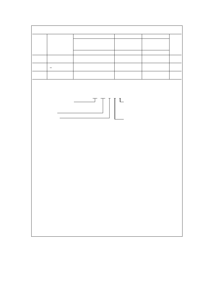
2

Logic Diagram
TL F 9482 � 4
Please note that this diagram is provided only for the understanding of logic operations and should not be used to estimate propagation delays
3
Absolute Maximum Ratings
(Note 1)
If Military Aerospace specified devices are required
please contact the National Semiconductor Sales
Office Distributors for availability and specifications
Storage Temperature
b
65 C to
a
150 C
Ambient Temperature under Bias
b
55 C to
a
125 C
Junction Temperature under Bias
b
55 C to
a
175 C
Plastic
b
55 C to
a
150 C
V
CC
Pin Potential to
Ground Pin
b
0 5V to
a
7 0V
Input Voltage (Note 2)
b
0 5V to
a
7 0V
Input Current (Note 2)
b
30 mA to
a
5 0 mA
Voltage Applied to Output
in HIGH State (with V
CC
e
0V)
Standard Output
b
0 5V to V
CC
TRI-STATE Output
b
0 5V to
a
5 5V
Current Applied to Output
in LOW State (Max)
twice the rated I
OL
(mA)
Note 1
Absolute maximum ratings are values beyond which the device may
be damaged or have its useful life impaired Functional operation under
these conditions is not implied
Note 2
Either voltage limit or current limit is sufficient to protect inputs
Recommended Operating
Conditions
Free Air Ambient Temperature
Military
b
55 C to
a
125 C
Commercial
0 C to
a
70 C
Supply Voltage
Military
a
4 5V to
a
5 5V
Commercial
a
4 5V to
a
5 5V
DC Electrical Characteristics
Symbol
Parameter
54F 74F
Units
V
CC
Conditions
Min
Typ
Max
V
IH
Input HIGH Voltage
2 0
V
Recognized as a HIGH Signal
V
IL
Input LOW Voltage
0 8
V
Recognized as a LOW Signal
V
CD
Input Clamp Diode Voltage
b
1 2
V
Min
I
IN
e b
18 mA
V
OH
Output HIGH
54F 10% V
CC
2 5
I
OH
e b
1 mA
Voltage
74F 10% V
CC
2 5
V
Min
I
OH
e b
1 mA
74F 5% V
CC
2 7
I
OH
e b
1 mA
V
OL
Output LOW
54F 10% V
CC
0 5
V
Min
I
OL
e
20 mA
Voltage
74F 10% V
CC
0 5
I
OL
e
20 mA
I
IH
Input HIGH
54F
20 0
m
A
Max
V
IN
e
2 7V
Current
74F
5 0
I
BVI
Input HIGH Current
54F
100
m
A
Max
V
IN
e
7 0V
Breakdown Test
74F
7 0
I
CEX
Output High
54F
250
m
A
Max
V
OUT
e
V
CC
Leakage Current
74F
50
V
ID
Input Leakage
74F
4 75
V
0 0
I
ID
e
1 9 mA
Test
All Other Pins Grounded
I
OD
Output Leakage
74F
3 75
m
A
0 0
V
IOD
e
150 mV
Circuit Current
All Other Pins Grounded
I
IL
Input LOW Current
b
0 6
mA
Max
V
IN
e
0 5V
I
OS
Output Short-Circuit Current
b
60
b
150
mA
Max
V
OUT
e
0V
I
CCL
Power Supply Current
12
20
mA
Max
V
O
e
LOW
4
AC Electrical Characteristics
74F
54F
74F
T
A
e a
25 C
T
A
V
CC
e
Mil
T
A
V
CC
e
Com
Symbol
Parameter
V
CC
e a
5 0V
C
L
e
50 pF
C
L
e
50 pF
Units
C
L
e
50 pF
Min
Typ
Max
Min
Max
Min
Max
t
PLH
Propagation Delay
4 5
8 1
10 5
4 5
14 0
4 5
12 0
ns
t
PHL
S
n
to Z
n
3 5
7 0
9 0
3 5
11 0
3 5
10 5
t
PLH
Propagation Delay
4 5
7 1
9 0
4 5
11 5
4 5
10 5
ns
t
PHL
E
n
to Z
n
3 0
5 7
7 0
2 5
9 0
2 5
8 0
t
PLH
Propagation Delay
3 0
5 3
7 0
2 5
9 0
3 0
8 0
ns
t
PHL
I
n
to Z
n
2 5
5 1
6 5
2 5
8 0
2 5
7 5
Ordering Information
The device number is used to form part of a simplified purchasing code where the package type and temperature range are
defined as follows
74F
153
S
C
X
Temperature Range Family
Special Variations
74F
e
Commercial
QB
e
Military grade device with
54F
e
Military
environmental and burn-in
processing
Device Type
X
e
Devices shipped in 13 reel
Package Code
Temperature Range
P
e
Plastic DIP
C
e
Commercial (0 C to
a
70 C)
D
e
Ceramic DIP
M
e
Military (
b
55 C to
a
125 C)
F
e
Flatpak
L
e
Leadless Chip Carrier (LCC)
S
e
Small Outline SOIC JEDEC
SJ
e
Small Outline SOIC EIAJ
5