54LCX16244
Low Voltage 16-Bit Buffer/Line Driver with 5V Tolerant
Inputs and Outputs
General Description
The LCX16244 contains sixteen non-inverting buffers with
TRI-STATE
Æ
outputs designed to be employed as a memory
and address driver, clock driver, or bus oriented transmitter/
receiver. The device is nibble controlled. Each nibble has
separate TRI-STATE control inputs which can be shorted to-
gether for full 16-bit operation.
The LCX16244 is designed for low voltage (3.3V) V
CC
appli-
cations with capability of interfacing to a 5V signal environ-
ment.
The LCX16244 is fabricated with an advanced CMOS tech-
nology to achieve high speed operation while maintaining
CMOS low power dissipation.
Features
n
5V tolerant inputs and outputs
n
Power down high impedance inputs and outputs
n
Supports live insertion/withdrawal
n
2.0V≠3.6V V
CC
supply operation
n
±
24 mA output drive
n
Implements patented noise/EMI reduction circuitry
n
Functionally compatible with 54 series 16244
n
ESD performance:
Human body model
>
2000V
Machine model
>
200V
n
Standard Microcircuit Drawing (SMD) 5962-9950501
Ordering Code
Order Number
Package Number
Package Description
54LCX16244W-QML
WA48A
48-Lead Cerpack Package
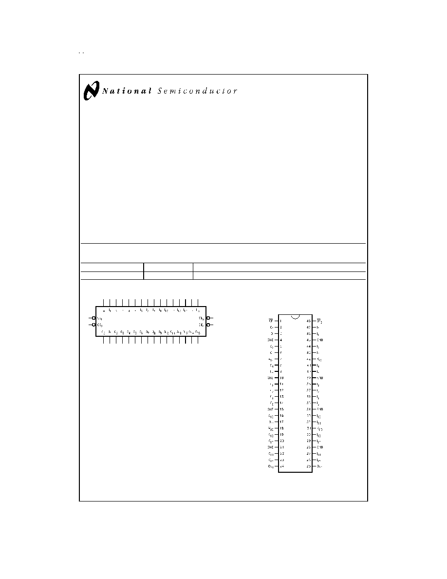
Logic Symbol
Connection Diagram
TRI-STATE
Æ
is a registered trademark of National Semiconductor Corporation.
DS101059-1
Pin Assignment for
Cerpack
DS101059-2
April 1999
54LCX16244
Low
V
oltage
16-Bit
Buffer/Line
Driver
with
5V
T
olerant
Inputs
and
Outputs
© 1999 National Semiconductor Corporation
DS101059
www.national.com
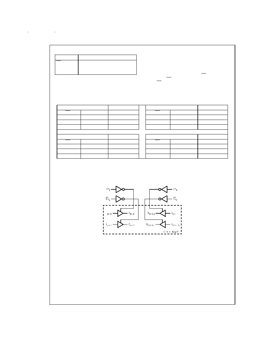
Pin Descriptions
Pin Names
Description
OE
n
Output Enable Input (Active Low)
I
0
≠I
15
Inputs
O
0
≠O
15
Outputs
Functional Description
The LCX16244 contains sixteen non-inverting buffers with
TRI-STATE standard outputs. The device is nibble (4 bits)
controlled with each nibble functioning identically, but inde-
pendent of the other. The control pins can be shorted to-
gether to obtain full 16-bit operation. The TRI-STATE outputs
are controlled by an Output Enable (OE
n
) input for each
nibble. When OE
n
is LOW, the outputs are in bi-state mode.
When OE
n
is HIGH, the outputs are in the high impedance
mode, but this does not interfere with entering new data into
the inputs.
Truth Tables
Inputs
Outputs
Inputs
Outputs
OE
1
I
0
≠I
3
O
0
≠O
3
OE
2
I
4
≠I
7
O
4
≠O
7
L
L
L
L
L
L
L
H
H
L
H
H
H
X
Z
H
X
Z
Inputs
Outputs
Inputs
Outputs
OE
3
I
8
≠I
11
O
8
≠O
11
OE
4
I
12
≠I
15
O
12
≠O
15
L
L
L
L
L
L
L
H
H
L
H
H
H
X
Z
H
X
Z
H = High Voltage Level
L = Low Voltage Level
X = Immaterial
Z = High Impedance
Logic Diagram
DS101059-3
www.national.com
2
Absolute Maximum Ratings
(Note 1)
If Military/Aerospace specified devices are required,
please contact the National Semiconductor Sales Office/
Distributors for availability and specifications.
Supply Voltage (V
CC
)
-0.5V to +7.0V
DC Input Voltage (V
I
)
-0.5V to +7.0V
DC Input Diode Current (I
IK
)
V
I
<
GND
-50 mA
DC Output Diode Current (I
OK
)
V
O
<
GND
-50mA
V
O
V
CC
+50mA
DC Output Voltage (V
O
) (Note 2)
Output in High or Low State
-0.5V to V
CC
+ 0.5V
Output in TRI-STATE
-0.5V to 7.0V
DC Output Source or Sink Current
(I
O
)
±
50mA
DC V
CC
or Ground Current
±
400mA
Storage Temperature Range
(T
STG
)
-65∞C to +150∞C
Power Dissapation
750mW
Junction Temperature (T
J
)
175∞C
Recommended Operating
Conditions
(Note 2)
Supply Voltage (V
CC
)
Operating
2.0V to 3.6V
Data Retention
1.5V to 3.6V
Input Voltage (V
I
)
0V to 5.5V
Output Voltage (V
O
)
High or Low State
0V to V
CC
TRI-STATE
0V to 5.5V
Operating Temperature (T
A
)
-55∞C to +125∞C
Minimum Input Edge Rate (
t/
V)
V
IN
from 0.8V to 2.0V, V
CC
= 3.0V
0ns/V to 10ns/V
Note 1: The Absolute Maximum Ratings are those values beyond which the
safety of the device cannot be guaranteed. The device should not be oper-
ated at these limits. The parametric values defined in the Electrical Charac-
teristics tables are not guaranteed at the Absolute Maximum Ratings. The
"Recommended Operating Conditions" table will define the conditions for ac-
tual device operation.
Note 2: I
O
Absolute Maximum Rating must be observed.
DC Electrical Characteristics
Symbol
Parameter
Conditions
V
CC
T
A
= -55∞C to +125∞C
Units
(V)
Min
Max
V
IH
HIGH Level Input Voltage
2.7≠3.6
2.0
V
V
IL
LOW Level Input Voltage
2.7≠3.6
0.8
V
V
OH
HIGH Level Output Voltage
I
OH
= -100 µA
2.7≠3.6
V
CC
- 0.2
V
I
OH
= -12 mA
2.7
2.2
V
I
OH
= -12 mA
3.0
2.4
V
I
OH
= -24 mA
3.0
2.2
V
V
OL
LOW Level Output Voltage
I
OL
= 100 µA
2.7≠3.6
0.2
V
I
OL
= 12 mA
2.7
0.4
V
I
OL
= 24 mA
3.0
0.55
V
V
IC
Negative Input Clamp
Voltage
I
IN
= -18mA
3.0
-1.2
V
I
I
Input Leakage Current
0
V
I
5.5V
2.7≠3.6
±
5.0
µA
I
OZ
3-STATE Output Leakage
0
V
O
5.5V
2.7≠3.6
±
5.0
µA
V
I
= V
IH
or V
IL
I
OFF
Power-Off Leakage Current
V
I
or V
O
= 5.5V
0
10
µA
I
CC
Quiescent Supply Current
V
I
= V
CC
or GND
2.7≠3.6
20
µA
3.6V
V
I
, V
O
5.5V
2.7≠3.6
±
20
µA
I
CC
Increase in I
CC
per Input
V
IH
= V
CC
-0.6V
2.7≠3.6
500
µA
www.national.com
3

AC Electrical Characteristics
Symbol
Parameter
T
A
= -55∞C to +125∞C, C
L
= 50pF, R
L
= 500
Units
V
CC
= 3.3V
±
0.3V
V
CC
= 2.7V
Min
Max
Min
Max
t
PHL
Propagation Delay
0.5
5.5
1.0
6.0
ns
t
PLH
Data to Output
0.5
5.5
1.0
6.0
t
PZL
Output Enable Time
0.5
6.5
1.0
7.0
ns
t
PZH
0.5
6.5
1.0
7.0
t
PLZ
Output Disable Time
1.0
6.0
1.0
6.0
ns
t
PHZ
1.0
6.0
1.0
6.0
t
OSHL
Output to Output Skew (Note 3)
1.0
1.0
ns
t
OSLH
Note 3: Skew is defined as the absolute value of the difference between the actual propagation delay for any two separate outputs of the same device. The speci-
fication applies to any outputs switching in the same direction, either HIGH to LOW (t
OSHL
) or LOW to HIGH (t
OSLH
). Parameter guaranteed by design.
Dynamic Switching Characteristics
Symbol
Parameter
Conditions
V
CC
(V)
T
A
= 25∞C
Units
Max
V
OLP
Quiet Output Dynamic Peak V
OL
C
L
= 50 pF, V
IH
= 3.3V, V
IL
= 0V
3.3
1.2
V
V
OLV
Quiet Output Dynamic Valley V
OL
C
L
= 50 pF, V
IH
= 3.3V, V
IL
= 0V
3.3
-1.1
V
Capacitance
Symbol
Parameter
Conditions
Max
Units
C
IN
Input Capacitance
V
CC
= Open, V
I
= 0V or V
CC
10
pF
C
OUT
Output Capacitance
V
CC
= 3.3V, V
I
= 0V or V
CC
12
pF
C
PD
Power Dissipation Capacitance
V
CC
= 3.3V, V
I
= 0V or V
CC
, f = 10 MHz
40
pF
www.national.com
4

Physical Dimensions
inches (millimeters) unless otherwise noted
LIFE SUPPORT POLICY
NATIONAL'S PRODUCTS ARE NOT AUTHORIZED FOR USE AS CRITICAL COMPONENTS IN LIFE SUPPORT
DEVICES OR SYSTEMS WITHOUT THE EXPRESS WRITTEN APPROVAL OF THE PRESIDENT OF NATIONAL
SEMICONDUCTOR CORPORATION. As used herein:
1. Life support devices or systems are devices or
systems which, (a) are intended for surgical implant
into the body, or (b) support or sustain life, and
whose failure to perform when properly used in
accordance with instructions for use provided in the
labeling, can be reasonably expected to result in a
significant injury to the user.
2. A critical component is any component of a life
support device or system whose failure to perform
can be reasonably expected to cause the failure of
the life support device or system, or to affect its
safety or effectiveness.
National Semiconductor
Corporation
Americas
Tel: 1-800-272-9959
Fax: 1-800-737-7018
Email: support@nsc.com
National Semiconductor
Europe
Fax: +49 (0) 1 80-530 85 86
Email: europe.support@nsc.com
Deutsch Tel: +49 (0) 1 80-530 85 85
English
Tel: +49 (0) 1 80-532 78 32
FranÁais Tel: +49 (0) 1 80-532 93 58
Italiano
Tel: +49 (0) 1 80-534 16 80
National Semiconductor
Asia Pacific Customer
Response Group
Tel: 65-2544466
Fax: 65-2504466
Email: sea.support@nsc.com
National Semiconductor
Japan Ltd.
Tel: 81-3-5639-7560
Fax: 81-3-5639-7507
www.national.com
48-Lead Cerpack
Package Number WA48A
54LCX16244
Low
V
oltage
16-Bit
Buffer/Line
Driver
with
5V
T
olerant
Inputs
and
Outputs
National does not assume any responsibility for use of any circuitry described, no circuit patent licenses are implied and National reserves the right at any time without notice to change said circuitry and specifications.