
TL F 6037
MM54C922MM74C922
16-Key
Encoder
MM54C923MM74C923
20-Key
Encoder
July 1993
MM54C922 MM74C922 16-Key Encoder
MM54C923 MM74C923 20-Key Encoder
General Description
These CMOS key encoders provide all the necessary logic
to fully encode an array of SPST switches The keyboard
scan can be implemented by either an external clock or
external capacitor These encoders also have on-chip pull-
up devices which permit switches with up to 50 kX on resist-
ance to be used No diodes in the switch array are needed
to eliminate ghost switches The internal debounce circuit
needs only a single external capacitor and can be defeated
by omitting the capacitor A Data Available output goes to a
high level when a valid keyboard entry has been made The
Data Available output returns to a low level when the en-
tered key is released even if another key is depressed The
Data Available will return high to indicate acceptance of the
new key after a normal debounce period this two-key roll-
over is provided between any two switches
An internal register remembers the last key pressed even
after the key is released The TRI-STATE
outputs provide
for easy expansion and bus operation and are LPTTL com-
patible
Features
Y
50 kX maximum switch on resistance
Y
On or off chip clock
Y
On-chip row pull-up devices
Y
2 key roll-over
Y
Keybounce elimination with single capacitor
Y
Last key register at outputs
Y
TRI-STATE outpust LPTTL compatible
Y
Wide supply range
3V to 15V
Y
Low power consumption
Connection Diagrams
Pin Assignment for
Dual-In-Line Package
TL F 6037 � 1
Top View
Order Number MM54C922 or
MM74C922
Pin Assignment
for SOIC
TL F 6037 � 14
Top View
Order Number MM74C922
Pin Assignment for
DIP and SOIC Package
TL F 6037 � 2
Top View
Order Number MM54C923 or
MM74C923
TRI-STATE
is a registered trademark of National Semiconductor Corporation
C1995 National Semiconductor Corporation
RRD-B30M105 Printed in U S A

Absolute Maximum Ratings
(Note 1)
If Military Aerospace specified devices are required
please contact the National Semiconductor Sales
Office Distributors for availability and specifications
Voltage at Any Pin
V
CC
b
0 3V to V
CC
a
0 3V
Operating Temperature Range
MM54C922 MM54C923
b
55 C to
a
125 C
MM74C922 MM74C923
b
40 C to
a
85 C
Storage Temperature Range
b
65 C to
a
150 C
Power Dissipation (P
D
)
Dual-In-Line
700 mW
Small Outline
500 mW
Operating V
CC
Range
3V to 15V
V
CC
18V
Lead Temperature
(Soldering 10 seconds)
260 C
DC Electrical Characteristics
Min Max limits apply across temperature range unless otherwise specified
Symbol
Parameter
Conditions
Min
Typ
Max
Units
CMOS TO CMOS
V
Ta
Positive-Going Threshold Voltage
V
CC
e
5V I
IN
t
0 7 mA
3 0
3 6
4 3
V
at Osc and KBM Inputs
V
CC
e
10V I
IN
t
1 4 mA
6 0
6 8
8 6
V
V
CC
e
15V I
IN
t
2 1 mA
9 0
10
12 9
V
V
Tb
Negative-Going Threshold Voltage
V
CC
e
5V I
IN
t
0 7 mA
0 7
1 4
2 0
V
at Osc and KBM Inputs
V
CC
e
10V I
IN
t
1 4 mA
1 4
3 2
4 0
V
V
CC
e
15V I
IN
t
2 1 mA
2 1
5
6 0
V
V
IN(1)
Logical ``1'' Input Voltage
V
CC
e
5V
3 5
4 5
V
Except Osc and KBM Inputs
V
CC
e
10V
8 0
9
V
V
CC
e
15V
12 5
13 5
V
V
IN(0)
Logical ``0'' Input Voltage
V
CC
e
5V
0 5
1 5
V
Except Osc and KBM Inputs
V
CC
e
10V
1
2
V
V
CC
e
15V
1 5
2 5
V
I
rp
Row Pull-Up Current at Y1 Y2
V
CC
e
5V V
IN
e
0 1 V
CC
b
2
b
5
m
A
Y3 Y4 and Y5 Inputs
V
CC
e
10V
b
10
b
20
m
A
V
CC
e
15V
b
22
b
45
m
A
V
OUT(1)
Logical ``1'' Output Voltage
V
CC
e
5V I
O
e b
10 mA
4 5
V
V
CC
e
10V I
O
e b
10 mA
9
V
V
CC
e
15V I
O
e b
10 mA
13 5
V
V
OUT(0)
Logical ``0'' Output Voltage
V
CC
e
5V I
O
e
10 mA
0 5
V
V
CC
e
10V I
O
e
10 mA
1
V
V
CC
e
15V I
O
e
10 mA
1 5
V
R
on
Column ``ON'' Resistance at
V
CC
e
5V V
O
e
0 5V
500
1400
X
X1 X2 X3 and X4 Outputs
V
CC
e
10V V
O
e
1V
300
700
X
V
CC
e
15V V
O
e
1 5V
200
500
X
I
CC
Supply Current
V
CC
e
5V
0 55
1 1
mA
Osc at 0V (one Y low)
V
CC
e
10V
1 1
1 9
mA
V
CC
e
15V
1 7
2 6
mA
I
IN(1)
Logical ``1'' Input Current
V
CC
e
15V V
IN
e
15V
0 005
1 0
m
A
at Output Enable
I
IN(0)
Logical ``0'' Input Current
V
CC
e
15V V
IN
e
0V
b
1 0
b
0 005
m
A
at Output Enable
CMOS LPTTL INTERFACE
V
IN(1)
Logical ``1'' Input Voltage
54C V
CC
e
4 5V
V
CC
b
1 5
V
Except Osc and KBM Inputs
74C V
CC
e
4 75V
V
CC
b
1 5
V
V
IN(0)
Logical ``0'' Input Voltage
54C V
CC
e
4 5V
0 8
V
Except Osc and KBM Inputs
74C V
CC
e
4 75V
0 8
V
V
OUT(1)
Logical ``1'' Output Voltage
54C V
CC
e
4 5V
2 4
V
I
O
e b
360 mA
74C V
CC
e
4 75V
2 4
V
I
O
e b
360 mA
V
OUT(0)
Logical ``0'' Output Voltage
54C V
CC
e
4 5V
0 4
V
I
O
e b
360 mA
74C V
CC
e
4 75V
0 4
V
I
O
e b
360 mA
Note 1
``Absolute Maximum Ratings'' are those values beyond which the safety of the device cannot be guaranteed Except for ``Operating Temperature Range''
they are not meant to imply that the devices should be operated at these limits The table of ``Electrical Characteristics'' provides conditions for actual device
operation
2

DC Electrical Characteristics
Min Max limits apply across temperature range unless otherwise specified (Continued)
Symbol
Parameter
Conditions
Min
Typ
Max
Units
OUTPUT DRIVE (See 54C 74C Family Characteristics Data Sheet) (Short Circuit Current)
I
SOURCE
Output Source Current
V
CC
e
5V V
OUT
e
0V
b
1 75
b
3 3
mA
(P-Channel)
T
A
e
25 C
I
SOURCE
Output Source Current
V
CC
e
10V V
OUT
e
0V
b
8
b
15
mA
(P-Channel)
T
A
e
25 C
I
SINK
Output Sink Current
V
CC
e
5V V
OUT
e
V
CC
1 75
3 6
mA
(N-Channel)
T
A
e
25 C
I
SINK
Output Sink Current
V
CC
e
10V V
OUT
e
V
CC
8
16
mA
(N-Channel)
T
A
e
25 C
AC Electrical Characteristics
T
A
e
25 C C
L
e
50 pF unless otherwise noted
Symbol
Parameter
Conditions
Min
Typ
Max
Units
t
pd0
t
pd1
Propagation Delay Time to
C
L
e
50 pF
(Figure 1)
Logical ``0'' or Logical ``1''
V
CC
e
5V
60
150
ns
from D A
V
CC
e
10V
35
80
ns
V
CC
e
15V
25
60
ns
t
0H
t
1H
Propagation Delay Time from
R
L
e
10k C
L
e
10 pF
(Figure 2)
Logical ``0'' or Logical ``1''
V
CC
e
5V R
L
e
10k
80
200
ns
into High Impedance State
V
CC
e
10V C
L
e
10 pF
65
150
ns
V
CC
e
15V
50
110
ns
t
H0
t
H1
Propagation Delay Time from
R
L
e
10k C
L
e
50 pF
(Figure 2)
High Impedance State to a
V
CC
e
5V R
L
e
10k
100
250
ns
Logical ``0'' or Logical ``1''
V
CC
e
10V C
L
e
50 pF
55
125
ns
V
CC
e
15V
40
90
ns
C
IN
Input Capacitance
Any Input (Note 2)
5
7 5
pF
C
OUT
TRI-STATE Output Capacitance
Any Output (Note 2)
10
pF
AC Parameters are guaranteed by DC correlated testing
Note 1
``Absolute Maximum Ratings'' are those values beyond which the safety of the device cannot be guaranteed Except for ``Operating Temperature Range''
they are not meant to imply that the devices should be operated at these limits The table of ``Electrical Characteristics'' provides conditions for actual device
operation
Note 2
Capacitance is guaranteed by periodic testing
Switching Time Waveforms
TL F 6037 � 3
T1
T2
RC T3
0 7 RC where R
10k and C is external capacitor at KBM input
FIGURE 1
TL F 6037 � 4
FIGURE 2
3
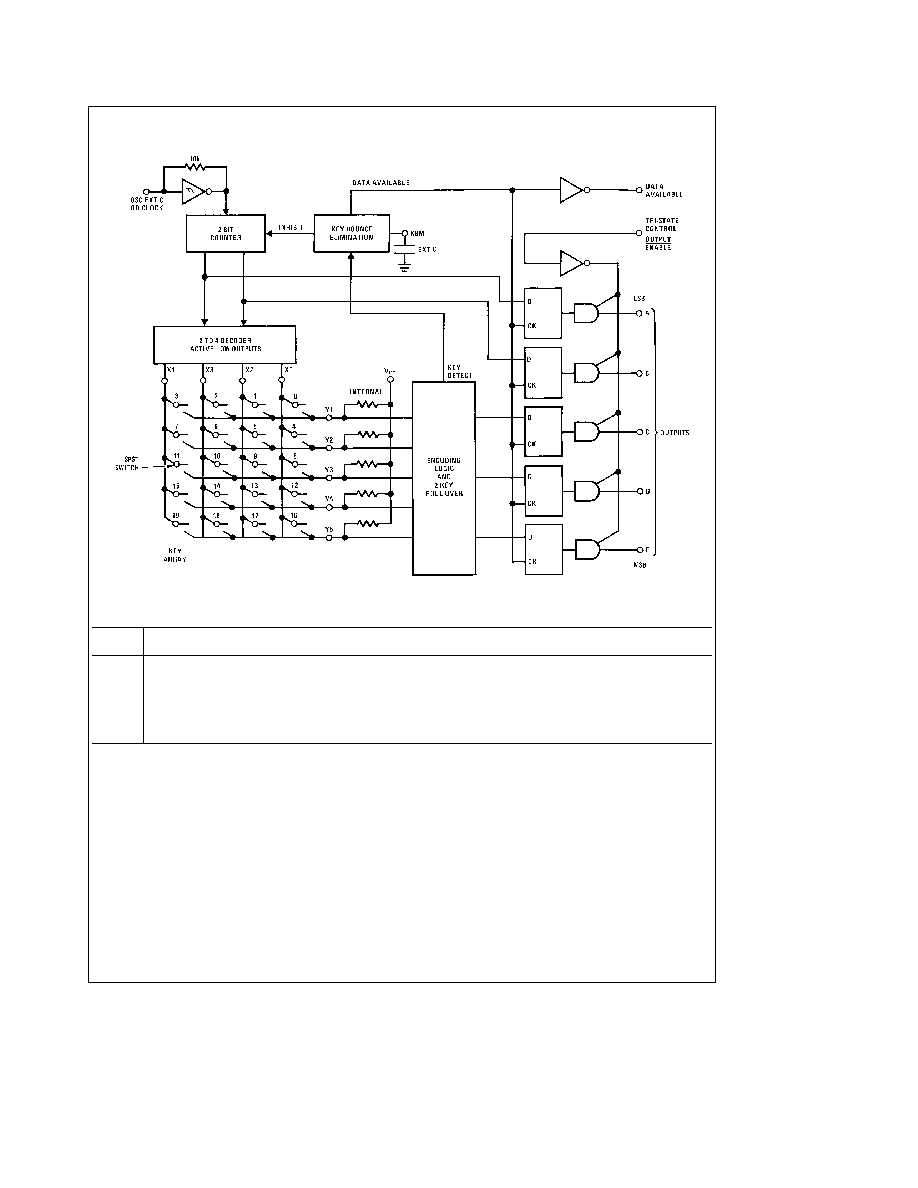
Block Diagram
TL F 6037 � 5
Truth Table
Switch
0
1
2
3
4
5
6
7
8
9
10
11
12
13
14
15
16
17
18
19
Position
Y1 X1 Y1 X2 Y1 X3 Y1 X4 Y2 X1 Y2 X2 Y2 X3 Y2 X4 Y3 X1 Y3 X2 Y3 X3 Y3 X4 Y4 X1 Y4 X2 Y4 X3 Y4 X4 Y5 X1 Y5 X2 Y5 X3 Y5 X4
D
A
A
0
1
0
1
0
1
0
1
0
1
0
1
0
1
0
1
0
1
0
1
T
B
0
0
1
1
0
0
1
1
0
0
1
1
0
0
1
1
0
0
1
1
A
C
0
0
0
0
1
1
1
1
0
0
0
0
1
1
1
1
0
0
0
0
O
D
0
0
0
0
0
0
0
0
1
1
1
1
1
1
1
1
0
0
0
0
U
E
0
0
0
0
0
0
0
0
0
0
0
0
0
0
0
0
1
1
1
1
T
Omit for MM54C922 MM74C922
4

Typical Performance Characteristics
Typical I
rp
vs V
IN
at
Any Y Input
TL F 6037 � 6
Typical R
on
vs V
OUT
at
Any X Output
TL F 6037 � 7
Typical F
SCAN
vs C
OSC
TL F 6037 � 8
Typical Debounce Period
vs C
KBM
TL F 6037 � 9
Typical Applications
Synchronous Handshake (MM74C922)
TL F 6037 � 10
Synchronous Data Entry Onto Bus (MM74C922)
TL F 6037 � 11
Outputs are enabled when valid entry is made and
go into TRI-STATE when key is released
Note 3
The keyboard may be synchronously scanned by omitting the capacitor at osc and driving osc directly if the system clock rate is lower than 10 kHz
5

Typical Applications
(Continued)
Asynchronous Data Entry Onto Bus (MM74C922)
TL F 6037 � 12
Outputs are in TRI-STATE until key is pressed then data is placed on bus
When key is released outputs return to TRI-STATE
Expansion to 32 Key Encoder (MM74C922)
TL F 6037 � 13
Theory of Operation
The MM74C922 MM74C923 Keyboard Encoders imple-
ment all the logic necessary to interface a 16 or 20 SPST
key switch matrix to a digital system The encoder will con-
vert
a
key
switch
closer
to
a
4(MM74C922)
or
5(MM74C923) bit nibble The designer can control both the
keyboard scan rate and the key debounce period by altering
the oscillator capacitor C
OSE
and the key bounce mask
capacitor C
MSK
Thus the MM74C922 MM74C923's per-
formance can be optimized for many keyboards
The keyboard encoders connect to a switch matrix that is 4
rows by 4 columns (MM74C922) or 5 rows by 4 columns
(MM74C923) When no keys are depressed the row inputs
are pulled high by internal pull-ups and the column outputs
sequentially output a logic ``0'' These outputs are open
drain and are therefore low for 25% of the time and other-
wise off The column scan rate is controlled by the oscillator
input which consists of a Schmitt trigger oscillator a 2-bit
counter and a 2 � 4-bit decoder
When a key is depressed key 0 for example nothing will
happen when the X1 input is off since Y1 will remain high
When the X1 column is scanned X1 goes low and Y1 will go
low This disables the counter and keeps X1 low Y1 going
low also initiates the key bounce circuit timing and locks out
the other Y inputs The key code to be output is a combina-
tion of the frozen counter value and the decoded Y inputs
Once the key bounce circuit times out the data is latched
and the Data Available (DAV) output goes high
If during the key closure the switch bounces Y1 input will
go high again restarting the scan and resetting the key
bounce circuitry The key may bounce several times but as
soon as the switch stays low for a debounce period the
closure is assumed valid and the data is latched
A key may also bounce when it is released To ensure that
the encoder does not recognize this bounce as another key
closure the debounce circuit must time out before another
closure is recognized
The two-key roll-over feature can be illustrated by assuming
a key is depressed and then a second key is depressed
Since all scanning has stopped and all other Y inputs are
disabled the second key is not recognized until the first key
is lifted and the key bounce circuitry has reset
The output latches feed TRI-STATE which is enabled when
the Output Enable (OE) input is taken low
6

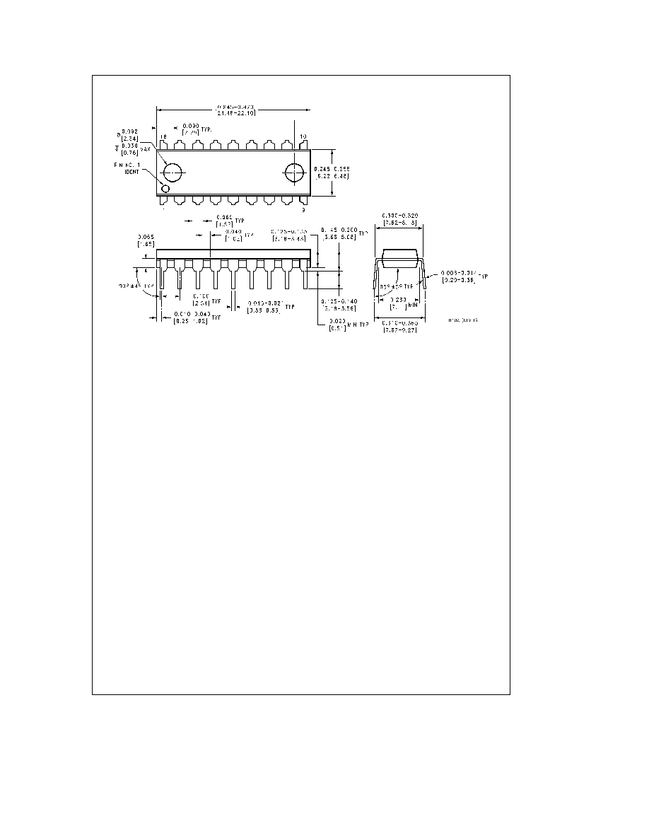
Physical Dimensions
inches (millimeters)
Ceramic Dual-In-Line Package (J)
Order Number MM54C922J or MM74C922J
NS Package Number J18A
Ceramic Dual-In-Line Package (J)
Order Number MM54C923J or MM74C923J
NS Package Number J20A
7

Physical Dimensions
inches (millimeters) (Continued)
Plastic Small Outline I C Package (M)
Order Number MM74C922M or MM74C923M
NS Package Number M20B
8
Physical Dimensions
inches (millimeters) (Continued)
Plastic Dual-In-Line Package (N)
Order Number MM54C922N or MM74C922N
NS Package Number N18A
9

MM54C922MM74C922
16-Key
Encoder
MM54C923MM74C923
20-Key
Encoder
Physical Dimensions
inches (millimeters) (Continued)
Plastic Dual-In-Line Package (N)
Order Number MM54C923N or MM74C923N
NS Package Number N20A
LIFE SUPPORT POLICY
NATIONAL'S PRODUCTS ARE NOT AUTHORIZED FOR USE AS CRITICAL COMPONENTS IN LIFE SUPPORT
DEVICES OR SYSTEMS WITHOUT THE EXPRESS WRITTEN APPROVAL OF THE PRESIDENT OF NATIONAL
SEMICONDUCTOR CORPORATION As used herein
1 Life support devices or systems are devices or
2 A critical component is any component of a life
systems which (a) are intended for surgical implant
support device or system whose failure to perform can
into the body or (b) support or sustain life and whose
be reasonably expected to cause the failure of the life
failure to perform when properly used in accordance
support device or system or to affect its safety or
with instructions for use provided in the labeling can
effectiveness
be reasonably expected to result in a significant injury
to the user
National Semiconductor
National Semiconductor
National Semiconductor
National Semiconductor
Corporation
Europe
Hong Kong Ltd
Japan Ltd
1111 West Bardin Road
Fax (a49) 0-180-530 85 86
13th Floor Straight Block
Tel 81-043-299-2309
Arlington TX 76017
Email cnjwge tevm2 nsc com
Ocean Centre 5 Canton Rd
Fax 81-043-299-2408
Tel 1(800) 272-9959
Deutsch Tel (a49) 0-180-530 85 85
Tsimshatsui Kowloon
Fax 1(800) 737-7018
English
Tel (a49) 0-180-532 78 32
Hong Kong
Fran ais Tel (a49) 0-180-532 93 58
Tel (852) 2737-1600
Italiano
Tel (a49) 0-180-534 16 80
Fax (852) 2736-9960
National does not assume any responsibility for use of any circuitry described no circuit patent licenses are implied and National reserves the right at any time without notice to change said circuitry and specifications